Note: Descriptions are shown in the official language in which they were submitted.
215g9.61
-
Case 1205
MINIATURISED ANTENNA FOR CONVERTING AN ALTERNATING
VOLTAGE INTO A MICROWAVE AND VICE VERSA,
NOTABLY FOR HOROLOGICAL APPLICATIONS
The present invention concerns antennas intended to
convert an alternating voltage into a microwave and vice
versa and, more particularly, antennas of this type
comprising a -conductive element and a ground plane
separated by a dielectric substrate. These antennas are
also known as microstrip patch antennas. The invention may
be used to emit and/or to receive GPS (Global Positioning
System) signals and, furthermore, it may be incorporated
in watches or in other horological products. The invention
will thus be described in the context of this exemplary
application. However, it will be understood that the
invention is of course not limited to this application.
The miniaturisation of antennas of the type described
above is generally accomplished by using a substrate
having a very high permitivity. This invariably implies
the use of a ceramic substrate. The fabrication costs of
such a substrate are often high.
In addition, miniaturised antennas of this type
possess a very narrow bandwidth. Consequently, due to
manufacturing tolerances, the design and construction of
these antennas is a difficult task. The mechanical
adjustment of the edges of the conductive element is a
technique which has been used for a long time to obtain
the desired resonance frequency of the antenna.
Nevertheless, such a solution is both destructive and
cumbersome .
An aim of the present invention is to provide a
miniaturised antenna of the type defined hereabove which
at least partially remedies the inconveniences of known
antennas.
Another aim of the invention is to supply a
miniaturised antenna of the type defined hereabove which
215g961 ,
~_ 2
is compact, and which is relatively simple and inexpensive
to manufacture.
Another aim of the invention is to supply a
miniaturised antenna of the type defined hereabove which
enables a simple adjustment of its resonance frequency.
Another aim of the invention is to supply a
miniaturised antenna of the type defined hereabove which
is suitable for use in a watch.
With this in mind, the object of the invention is an
antenna for converting an alternating voltage, supplied by
an antenna circuit, into a linearly polarised wave and
vice versa, comprising :
- a first dielectric substrate having two opposing
sides;
- a conductive element fixed on a first side of
said first dielectric substrate, said conductive element
being delimited at its periphery by an edge which provides
this element with a double planar symmetry according to
two perpendicular axes; and
- a ground plane fixed to the second side of said
first dielectric substrate;
said conductive element comprising an excitation point by
which it is connected to said antenna circuit, this latter
supplying said alternating voltage between the excitation
point and the ground plane;
said excitation point being located on a first of said
axes;
said antenna being characterised in that said conductive
element includes :
- a first pair of slots which extends, along the
second of said axes, from the periphery towards the center
of said conductive element.
Another object of the invention is to provide an
antenna for converting an alternating voltage from an
antenna circuit, into a linearly of circularly polarised
wave and vice versa, comprising :
2159961
~- 3
- a first dielectric substrate including two
opposlng sides;
- a conductive element fixed to a first side of
said first dielectric substrate, said conductive element
being delimited at its periphery by an edge which provides
this element with a double planar symmetry along two
perpendicular axes; and
- a ground plane fixed to this second side of said
first dielectric substrate;
said conductive element including an excitation point by
which it is connected to said antenna circuit, this latter
providing said alternating voltage between the excitation
point and said ground plane;
said excitation point being located on a third axis
bisecting the angle formed between the first and second
axes;
said antenna being characterised in that said conductive
element includes :
- a first pair of slots which extends, along the
first of said axes, from the periphery towards the center
of said conductive element; and
- a second pair of slots which extends, along -said
second axes, from the periphery towards the center of said
conductive element.
Due to these characteristics, the invention enables
the realisation of a miniaturised antenna without
requiring the utilisation of a substrate having a high
permitivity.
According to one embodiment, the antenna according to
the invention further comprises a frequency adjustment
plate, the distance between the periphery and the center
of said plate along said second axis varying as a function
of the angular rotation of the frequency regulating plate
around an axis perpendicular to the plane of the plate and
passing through its center with respect to said conductive
element.
21~g961
As a result of the foregoing, the rotation of the
frequency adjustment plate around the third axis enables a
simple and a precise adjustment of the resonant frequency
of the antenna, and this on a bandwidth greater than the
bandwidth of the conductive element.
Other characteristics and advantages of the invention
will appear during the description which will now follow,
provided as an example only, and made with reference to
the annexed drawings in which :
- Figure 1 is a cross-sectional view of an antenna
according to the present invention;
- figure 2 is a perspective view of the antenna of
figure l;
- figure 3 is a plan view of the conductive element
of the antenna of figures 1 and 2;
- figure 4 is a plan view of a variant of the
realisation of the conductive element of figure 3;
- figure 5 is a plan view of a frequency adjustment
plate intended to adjust the resonance frequency of the
antenna of figure l;
- figure 6 is a first variant of the realisation of
the frequency adjustment plate of figure 5;
- figure 7 is a second variant of the realisation
of the frequency adjustment plate of figure 5;
- figure 8 is a third variant of the realisation of
the frequency adjustment plate of figure 5;
- figure 9 is an exploded perspective view of
another antenna according to the inventioni
- figure 10 is a cross-sectional view of the
antenna of figure 9;
- figure 11 is a plan view of another variant of
the realisation of the conductive element of the
inventlon;
- figure 12 is a plan view of another variation of
the realisation of the conductive element of the
invention;
215gg61
-
- figure 13 is a plan view of another variant of
the realisation of the frequency adjustment plate of
figure 5;
- figure 14 is a plan view of another variant of
the realisation of the frequency adjustment plate of
figure 5;
- figure 15 is a plan view of another variant of
the frequency adjustment plate of figure 5;
- figure 16 is a plan view of the assembly of the
frequency adjustment plate of figure 13 and the conductive
element of figure 12;
- figure 17 is a plan view of the assembly of the
frequency adjustment plate of figure 15 and the conductive
element of figure 11;
- figure 18 is a plan view of the assembly of the
frequency adjustment plates of figures 7 and 8 and the
conductive element of figure 4;
- figure 19 is plan view of the assembly of the
frequency adjustment plate of figure 5 and the conductive
element of figure 3; and
- figure 20 is a cross-sectional view of a watch
including an antenna according to the present invention.
The assembly of the miniaturised antenna 1 according
to the invention represented in figures 1 and 2 comprises
a dielectric substrate 2, a conductive element 3 and a
ground plane 4. The conductive element 3 has the general
form of a disk and is called a "radiating patch". The
conductive element 3 and the ground plane 4 form are
deposited on opposing surfaces of the dielectric substrate
2. The antenna 1 has a geometry suitable for receiving and
emitted linearly polarised waves.
The conductive element 3 includes slots 5 and 6 which
are diametrically opposed and aligned along the axis 7.
The slots 5 and 6 extend from the periphery towards the
center of the conductive element 3. An excitation point 8
is situated in the plane of the conductive element 3, on
an axis 9 which is perpendicular to the axis 7. The
215g961
excitation is provided by means of a coaxial cable whose
central conductor 10 passes through the substrate 2 and is
soldered to the conductive element 3 at the position of
the excitation point 8.
Figure 3 shows more precisely the geometry of the
conductive element 3. It can be seen that the slots S and
6 both have a length rx and that the conductive element 3
has a diameter 2R, R being the radius of this latter.
The slots 5 and 6 constitute a capacitive charge for
the antenna 1. The theorical considerations, which will
not be considered here because they do not concern the
context of the present invention, show that the resonant
frequency of the antenna 1 strongly depends upon the
length rx of the slots 5 and 6. According to these
considerations, when rx is zero, the antenna 1 resonates
at a frequency fc. However, when the value of rx
approaches R, the resonant frequency approaches fc/2.
Furthermore, it is known that the diameter 2R of the
antenna is a function of the inverse of the resonant
frequency fc thereof. As the resonant frequency fc
approaches fc/2 for a certain length 2R, one may also
choose to reduce the length 2R in a half for a certain
resonant frequency fc. That is to say, one can reduce the
maximum size of the antenna 1 by a factor of 2 when the
slots extend substantially along the entire distance
separating the periphery from the center of the conductive
element. It will be noted in this regard the slots 5 and 6
may be realised by cutting the conductive element 3 by
means of a laser beam. Of course, the slots 5 and 6 may
also be realised by etching or any other chemical or
mechanical treatment of the conductive element 3.
It should be noted that this circular form of the
conductive element of figure 2 and 3 only represents one
example of a form of the conductive element of the
invention. A square form may also be used, as well as all
other conductive elements which are delimited at their
215g961
_ 7
periphery by an edge which provide to these elements with
a double planar symmetry along two perpendicular axes.
In a case of a linearly polarised antenna, the
excitation point is located on one of the two axes of
symmetry of the conductive element and the slots 5 and 6
extend along the other axis of symmetry.
Figure 4 shows the geometry of a conductive element
20 for receiving and emitting circularly polarised signals
as well as linearly polarised signals. The conductive
element 20 includes slots 21 and 22 which extend from its
periphery towards the center and which are aligned on a
same axis 23. As well, the conductive element 20 includes
slots 24 and 25 which extend from its periphery towards
the center and which are aligned on a same axis 26
perpendicular to the axis 23. An excitation point 27 is
located on an axis shifted by 45 with respect to the two
axis 23 and 24.
In order that the antenna has a linear polarisation,
the lengths rx of the slots 21 and 22 and ry of the slots
24 and 25 must be equal. However, a right-hand circular
polarisation is obtained if, for an excitation point 27
such as just described hereabove, rx is greater than ry by
a suitable amount. It will be understood that the circular
form of the conductive element 20 of figure 4 only
represents a particular form of the conductive element of
the invention. Needless to say, a square form may be used
or any other shape of conductive element delimited at its
periphery by an edge which provide it with a double planar
symmetry according to two perpendicular axis. In the case
o~ a circular or linearly polarised antenna, as, f~r
example, an antenna including a conductive element 20 of
figure 4, the excitation point 27 of the conductive
element is located on an axis bisecting of the angle
formed between the two axis of symmetry. In this case, the
pairs of slots 21, 22 et 23, 24 extend respectively along
the two axis of symmetry.
215g961
-
The resonant frequency of the antenna according to
the invention varies as a function of the distance r, if
one considers the conductive element 3 of figure 3, or as
a function of the distances rx and ry~ if one considers
the conductive element shown in figure 4. As will be seen
from the following, by using one or more frequency
adjustment plates of a particular shape as upper layer,
one can effectively vary the distances r, and the case
being the distances rx and ry~ by a simple rotation of the
plate.
Figures 5, 6, 7 and 8 show respectively examples 30,
31, 32 and 33 of geometries of such a frequency adjustment
plate, the distance between the periphery and the center
of said plate, along at least one of the axis defined by
the slots of the conductive element, varying as a function
of the angle of rotation of the plate about an axis A
perpendicular to the plane of the plate and passing
through the center of the plate with respect to the
conductive element. The structure shown in figures 5 to 8
may be realised in several ways. For examples, they may be
printed on a dielectric substrate or machined from a block
of metal. Several shapes of plates may be envisaged and
the choice thereof depends on the necessary tuning range
as well as the tuning resolution.
An electric contact with the surface of the
conductive element is not necessary as the principal of
varying the capacity through the slots also operates when
the plate and the conductive element are insulated from
each other. Thus, if one wishes to maintain an electric
contact, the contact must be uniform for all these slots,
which complicates the design of the frequency adjustment
plate. As a consequence, it is relatively simple to obtain
an appropriate insulation by using a dielectric plate or
air-gap between the frequency adjustment plate and the
slots of the conductive element. In addition, it will be
noted that in this case, the resonant frequency is less
sensitive to variations of rx and ry~
215~g61
~- 9
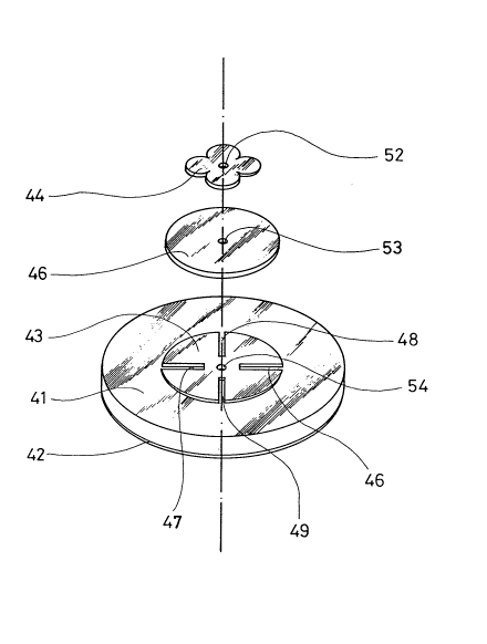
Figures 9 and 10 show an antenna 40 including a
dielectric substrate 41, a ground plane 42, a conductive
element 43 and a frequency adjustment plate 40, this
latter being separated from the conductive element 43 by
another dielectric substrate 45. The conductive element 43
includes an orthogonal slots 46, 47, 48 and 49. The
rotation of the frequency adjustment plate 44 about the
axis A with respect to the conductive element 43 modifies
the effective lengths of the slots 46 to 49 and, by
consequence, modifies the resonance frequency of the
antenna 40.
The antenna 40 further includes a coaxial connector
whose central conductor 50 passes through the substrate
41. The central connector 50 is soldered to the conductive
element 43, whilst the external conductor is soldered to
the ground plane 42. The two conductors of the coaxial
connector are also connected to an antenna circuit. The
antenna 40 converts an alternative voltage from the
antenna circuit, between the two conductors of the coaxial
connector, into a microwave and vice versa.
Moreover, the antenna 40 includes a central support
51 which passes through openings 52, 53 and 54 in the
center of the structure shown into figure 9 and which
maintains the alignment of the different elements of the
antenna 40. The central support 51 may be realised in an
insulating material or a conducting material, the
difference linked to the use of one or the other of these
two materials being a small change in the resonance
frequency. This difference may be compensated in any event
by a rotation of the frequency adjustment plate 44.
It will be noted that the center of the conductive
element 43 is a zero voltage point and that the fact that
this point is in open circuit or in short circuit with the
ground plan does not affect the characteristic of the
antenna. Preferably, a metallic central support may be
used since in this case the electrostatic potential of the
conductive element 43 and that the frequency adjustment
2159961
:W
plate 44 are that of the earth. This may be advantages
from the point of view of the electromagnetic
compatibility of the antenna 40.
When the length rx of the slots 21 and 22 and the
length ry of the slots 24 and 25 of figure 4 are equal,
the conductive element 20 is linearly polarised along a
line passing through the center of the conductive element
20 and through the excitation point 27. By using a
frequency adjustment plate such has that shown in figure 7
or in figure 9, one may adjust this linear polarisation.
Nevertheless, a circular polarisation of the antenna
having a single excitation point requires the introduction
of an asymmetry in the conductive element 20 so that two
orthogonal modes of resonance may be established. One
manner is which this may be done consists of introducing
perturbation segments in the conductive element 20.
Several examples of the shape of these perturbation
segments are shown by the references 60, 61, 62 and 63 of
the conductive elements 64 and 65 of figures 11 and 12.
This perturbation segments 60 to 63 may then be cut away
to introduce the desired symmetry.
In certain applications, the adjustment of the
resonant frequency of an antenna is only required to
overcome uncertainty of the value of the permitivity of
the substrate. In these cases, the antenna may be adjusted
by using the perturbation segments which have just been
described. Single narrow band frequency adjustment plates
may be used so that the antenna may be tuned to a desired
frequency.
Figures 13, 14 and 15 show examples of the shape o~
plates 70, 71 and 72. Figure 16 shows the assembly of the
frequency adjustment plate 70 of figure 13 and the
conductive element 65 of figure 12. Figure 17 shows the
assembly of the frequency adjustment plate 72 of figure 15
and the conductive element 64 of figure 11. It will be
noted that the shape and the size of the frequency
adjustment plates 70, 71 and 72 with respect to the
2159g61
ll
corresponding conductive elements are such that the
distance from the periphery to the center of the plates
70, 71 and 72 varies only slightly as a function of the
angle of rotation.
This asymmetry may also be introduced, in the case
where the structure of the antenna is such that the length
of the slots rx and ry have the same value, by using a
combination of two frequency adjustment plates. Figure 18
shows an example of such a combination of plates. In this
example, the frequency adjustment plates 32 and 33,
respectively shown in figure 7 and 8, are supported above
the conductive element 20 of figure 4. One may firstly
turn the frequency adjustment plate 32 to establish a
linear polarisation and a desired frequency. Next, the
frequency adjustment plate 33 may be turned to introduce a
control difference between the length rx and ry, which
leads the antenna to a circularly polarised operation.
Advantageously, the use of two frequency adjustment plates
enables the use of greater antenna manufacturing
tolerances.
This description will now be completed by referring
to practical examples of the construction of an antenna
according to the invention. As the antennas were conceived
by using a digital plane which divides the surface of the
conductive element into scared cells, the dimensions
expressed in these examples are in terms of "cell size ~".
Example 1 : Linear ~olarisation and larqe bandwidth
adjustment
A conductive element having the shape represented in
figure 3 is edged from a substrate in a material sold by
the commercial name ~LTRALAM~. The initial dimensions of
the substrate were 144 x 1.5 mm3 and its relative
permitivity was 2.5. A circular hole having a diameter of
1 mm was pierced through the center of the substrate. The
antenna is excited by means of a signal applied to the
2159~61
12
conductive element 3 via a standard 50 Q SMA coaxial
cable. The dimensions of the conductive element are the
following :
~ = 40/61 mm, 2R = 30.5 ~, r = 19 ~, w = 0.5 ~, yf = 7 ~.
Furthermore, a hole having a diameter equal to 3 ~ is
formed in the center of the conductive element.
A frequency adjustment plate having the shape shown
in figure 5 was used. The assembly of the antenna is shown
in figure 19. The frequency adjustment plate is etched
from a circular epoxy disk. This material was chosen for
its high rigidity. The circular disk has a thickness of
0.8 mm and a diameter of 60 mm. Another disk was also used
in epoxy such as that reference 45 in figure 9. This disk
acts as a spacing disk between the conductive element and
the frequency adjustment plate. The spacing plate has a
thickness of 0.1 mm and a diameter of 25 mm.
The resonant frequency of the antenna was measured
and it was observed that this frequency varied between
2.118 GHz (when the angle 01 = 90) and 2.448 GHz (when
the angle 01 = 0). This variation corresponds to a
frequency adjusting span of 14.5%. The voltage standing-
wave ratio, measured at the resonant frequency, is better
than twice the total of the band. The radiation pattern
were measured in an echoic chamber at three different
frequencies, that is, 2.118, 2.296 and 2.448 GHz, these
three frequencies corresponding respectively to three
different angular positions of the frequency adjusting
structure. The co-polarisation diagrams are in these cases
substantially the same as the co-polarisation diagrams for
a circular conductive element. In addition, the cross-
polarisation levels are less than -20 dB, which indicates
that the frequency adjusting structure does not introduce
any level of any unacceptable crossed polarisation
radiation.
21~9961
It will be noted that the angle of rotation of the
frequency adjustment plate 33 of the antenna represented
in figure 19 is limited to a value of 90. However, the
use of the frequency adjustment plate represented in
figure 6 enables a rotation of an angle of 180 and by
consequence a final adjustment of the frequency in the
same frequency range.
Example 2 : Circular ~olarisation and wide band adiustment
An antenna was manufactured having an assembly such
as that shown in figure 18. This antenna was excited at a
single point situated on the axis bisecting the angle
formed between the two orthogonal axes of the slots of the
conductive element. It is known that this excitation
technique is quite sensitive with respect to other known
techniques and that it requires a precise separation
between the two degenerate modes of the antenna. In
particular, the two resonance frequencies must be
separated by a frequency a where
2~f
o~ =
(~ + f~)
and where ~ is the bandwidth of the conductive element at
the resonance frequency fc during the treatment of a
circularly polarised signal in the case where the voltage
standing-wave ratio is equal to 2. The geometry of the
conductive element represented in figure 4 may be adapted
to this end by using an asymmetric frequency adjusting
structure. A circular polarisation excitation requires and
an asymmetry in the length of the slots of the conductive
elements. In particular, in the case of a conductive
element which is excited at a point located in the third
sector, such as it is the case in figure 18, the fact that
the length rx is greater than the length ry leads to a
right-hand circular polarisation.
2159961
14
Practical experiences have shown that the bandwidth
of the antenna varies as a function of the frequency
adjustment. This variation may complicate the design of a
simple frequency adjustment plate since a precise
knowledge of its effect required. The use of two frequency
adjustment plates, such as the two plates shown in figure
18, may at least partially overcome this problem. In
addition, the-use of two frequency adjustment plates
enables greater antenna manufacturing tolerances to be
used.
In this example, the conductive element is etched
from a substrate of a material sold under the commercial
name of ULTRALAM~. The initial dimensions of the substrate
were
144 x 144 x 1.5 mm3 and its relative permitivity was 2.5.
A circular hole of diameter of 1 mm was pierced at the
center of the substrate. The antenna is excited by means
of a signal applied to the conductive element 3 via a
standard 50 Q SMA coaxial cable. The dimensions of the
conductive element are the following :
= 40/66 mm, 2R = 30.5 ~, rx = ry = 19 ~, w = 0.5 ~,
Xf = yf = 7 ~.
In addition, a hole having a diameter equal to 3 ~ is
provided at the center of the conductive element.
Frequency adjustment plates having the form shown
figures 7 and 8 are used. The assembly of the antenna is
shown in figure 18. The frequency adjustment plates of
figure 7 are etched from a circular epoxy disc. The
circular disc has a thickness of 0.1 mm and a diameter of
60 mm. The frequency adjustment plate of figure 8 is also
etched from a circular epoxy disc. The circular disc has a
thickness of 0.8 mm and a diameter of 50 mm. Another epoxy
disc, such as that shown by the reference numeral 45 in
figure 9, is used as spacing disc and is located when the
conductive element and the frequency adjustment plate. The
2159961
spacing disc has a thickness of 0.1 mm and a diameter of
25 mm. No spacing disc is used between the two frequency
adjustment plates.
The adjustment range of the resonant frequency of the
antenna is slightly less than the adjustment range of the
preceding example due to the shift between the two
degenerate modes of the antenna in the second example.
This variation is of the order of 10%. The voltage
standing-wave ratio, measured at resonance, is better than
2 as a frequency of 2.306 MHz.
Whilst the assembly shown in figure 18 creates a
right-hand circular polarisation, it will be noted that
the rotation of the plate 33 of an angle of 90 creates a
left-hand circular polarisation.
Exam~le 3 : Circular ~olarisation and narrow band
adjustment
- A conductive element having the form represented in
figure 11 is edged from a substrate in a material sold
under the commercial name TMM-10~, this conductive element
including perturbation segments enabling a right-hand
circular polarisation operation. The substrate is circular
and has a diameter of 34.5 mm. The thickness of the
substrate is 0.635 mm and its relative permitivity is 9.2.
A circular hole having a diameter of 1.4 mm is pierced in
the center of the substrate. The antenna is excited by
means of a signal applied to the conductive element via a
standard 50 Q SMA coaxial cable. The dimensions of the
conductive element are the following : -
2R = 14.75 mm, rx = ry = 9.5 mm, w = 0.25 mm,
Xf - yf = 3.5 mm.
Furthermore, a hole having a diameter equal to 1.693 mm is
pierced in the center of the conductive element.
2159961
_
16
A frequency adjustment plate having the shape shown
into figure 15 was used. The assembly of the antenna is
shown in figure 17. The frequency adjustment plate was
edged from a circular epoxy disc. This material is
preferred here due to its great rigidity. The circular
disc has a thickness of 0.8 mm and a diameter of 25 mm. A
dielectric disc in TEFLON~ is used as spacing disc and is
located between a conductive element and the frequency
adjustment plate. This spacing disc has a thickness of
0.254 mm and a diameter of 25 mm. This structure enables a
frequency adjustment range to be obtained of the order of
2 %.
The antenna i5 adjusted to the frequency of the GPS
signals (1.57542 GHz) by the rotation of the frequency
adjustment plate. The measured axial ratio is 2.54 dB and
the bandwidth, with a voltage standing-wave ratio equal to
2, is 12 MHz. The measured amplification is -6 dBi.
Exam~le 4 : Circular polarisation and narrow band
adiustment
This example uses a conductive element comprising
perturbation segments for a right-hand circular
polarisation operation. A conductive element having the
form shown in figure 12 is edged from a substrate of
TMM-10~. The substrate is circular and has a diameter of
34.5 mm. The thickness of the substrate is 1.27 mm and its
relative permitivity is 9.2. A circular hole of diameter
of 1.4 mm is pierced at the center of the substrate. The
antenna is excited by means of a signal applied to the
conductive element via a standard of 50 Q SMA coaxial
cable. The dimensions of the conductive element are the
following :
2R = 14.7 mm, rx = ry = 10.12 mm, w = 0.25 and
Xf = yf = 1.93 mm.
2159961
~_ 17
Furthermore, a hole having a diameter equal to 1.631 mm is
pierced in the center of the conductive element.
A frequency adjustment plate having the form shown in
figure 13 is machined from a copper block. No spacing disc
is used, but an air-gap is created by supporting the
frequency adjustment plate at 0.2 mm above the conductive
element by means of a central support element. The
assembly of the antenna is illustrated in figure 16.
In this example, the frequency adjustment plate may
be turned by 90 to obtain a frequency adjustment range of
6 ~. The geometry of the frequency adjustment plate 70 is
such that the distance between its periphery and its
origin vary linearly between 4.5 mm and 8.75 mm as a
function of the angle of rotation thereof.
The antenna of this example is mounted in a plastic
case and is tuned to the frequency of GPS signals
(1.57542 GHz) by rotation of the frequency adjustment
plate. The measured axial ratio, with the case fixed to
the earth plate of the antenna, is 1.78 dB and the
bandwidth when the voltage standing-wave ratio is equal to
2 is 11 MHz. The measured gain is -4.0 dB.
According to a variation of this embodiment, the
frequency adjustment plate 70 may be replaced by the
frequency adjustment plate 71 of figure 14. This frequency
adjustment plate is easy to manufacture as it may be
realised from parallelepiped bars currently available in
industry. The adjustment range in this case is of the
order of 3 ~ and the maximum rotation angle is 45.
The invention enables a certain number of interesting
applications. Firstly, the geometry of the conductive
elements enables a suitable control of its size. Current
shapes such as circular or rectangular shapes have a fixed
size according to the desired resonant frequency and
according to the characteristics of the substrate used. By
using a variable slotting, the dimensions of the antenna
may be modified by a factor of 2. Furthermore, the shape
of the conductive element enables an optimal use of the
2159961
_
18
available surface, since there is only a very small non-
metallised surface. As a consequence, the invention
enables a miniaturisation of the antenna whilst
maintaining an optimal amplification/size ratio.
The examples 3 and 4 described above of the antennas
are intended to receive GPS waves transmitted by
satellite. The dimensions of the antenna are such that it
may be mounted-in a watch case. In a watch, the antenna
may for example be located between the motor and the
hands.
Figure 20 is a cross-sectional view of watch 80
comprising a watch case 81, a back 82 and a crystal 83.
The watch 80 includes a dielectric substrate 85, an earth
plate 86 connected to the watch case 81, a conductive
element 87 and a fre~uency element adjustment plate 88,
this latter being separated by the conductive element 87
by a further dielectric substrate 89. The conductive
element includes two pairs of orthogonal slots. The length
of one of this pair of slots is greater than the length of
the other pair in order to assure a circular of the
polarisation of the antenna 87. The rotation of a
frequency adjustment plate 88, with respect to the
conductive element 87 notify the length of the two pairs
of orthogonal slots and, consequently, modifies the
resonance frequency of the antenna 84.
The watch 80 further includes a coaxial cable 90
whose central conductor passes through the dielectric
substrate 85. This central conductor is soldered to the
conductive element 87, whilst the external conductor is
soldered to the ground plane 86. The two conductors of the
coaxial cable are also connected to an antenna circuit 91,
located in the watch 80, between the back 82 and the earth
plane 86.
Furthermore, the watch 80 includes a central support
92 on which are mounted the hour, minute and second hands,
respectively 93, 94 and 95. The central support 92 is
connected to horological movement 96 which is also located
2159961
19
between the back 82 and the earth plane 86. The
horological movement 96 drives the hands 93 to 95 of the
watch 80 by means of the central support 92 in order to
indicate the standard time. In addition, the central
support 92 acts to maintain the alignment of the various
elements 85 to 88 of the antenna 80.
The near environment of the antenna 80 has a certain
effect on the resonant frequency of the antenna. In this
respect, the angular positions of the hands 93 to 95 with
respect to the slots of the conductive elements 87 have a
certain effect on the resonance frequency of the antenna.
To compensate this effect, during the reception or
transmission of a signal by the antenna 80, the hands 93
to 95 are brought by the horological movement 96 in
angular positions which have little influence on the
resonance frequency of the antenna 80.
Preferably, these angular positions are such that
none of the hands 93 to 95 are superposed with the slots
of the conductive element 87. In addition, the hands 93 to
95 may be brought into the same angular position during
each reception/transmission, in order that the influence
of the hands 93 to 95 cn the resonance frequency of the
antenna 80 is always the same.
The adjustment structures of the resonance frequency
of the antenna which has just been described, enable
firstly, a compensation of the non-homogeneity of the
characteristics of the substrate material and secondly an
adjustment of the frequency over a wide band. In additioni
the dimensions of the antenna remain minimal since the
frequency adjustment structure only very slightly increase
the thickness of the antenna.
It will be noted that in order to obtain such a size
with a known circular antenna, it is necessary to use a
substrate having a relative permitivity of the order of
15. Such a permitivity necessitates the use of a ceramic
substrate and leads to high manufacturing costs. It will
also be noted that these ceramic substrates have further
215g961
characteristics in many applications. For example, the
near environment of the antenna has a certain effect on
the resonance frequency of the antenna. This effect may be
compensated by a simple rotation of the frequency
regulating plate of the antenna. In this respect, the
hands of a watch including the antenna of the invention
are, preferably, realised in plastic, or in any other non
metallic material, to reduce this effect.
Finally, it should be noted that many modifications
may be brought to the antenna according to the invention
without departing from the domain thereof.
In that respect, it will be appreciated that the
invention may also be used in a watch comprising digital
display means rather than the analog display means shown
in figure 20.