Note: Descriptions are shown in the official language in which they were submitted.
CA 02164351 1999-04-27
LAMINATED CYLINDRICAL BACKPLANE
Cross Reference to Related Invention
This application is related to commonly assigned U.S. Patent No. 5,716,220,
entitled
"Backplane Arrangement For Electrical Equipment", which issued on February 10,
1998.
Background of the Invention
FIG. 1 illustrates a prior art backplane arrangement. Backplane 10 comprises
upper
connectors 12 and lower connectors 14. Contacts 16 within each connector pair,
12 and 14,
mate with contacts on the surface of a circuit card. The contacts on the
surface of the circuit
card are positioned near the edge of the card so that they make contact with
electrical
contacts 16 when the card edge is inserted into the connector. Backplane 10
typically
includes conductors that connect corresponding contacts on each of the
connectors to create
a bus structure. For example, contacts 18, 20, 22 and similarly positioned
contacts of
connectors 12, are connected through the conductors of backplane 10. This
arrangement
provides a convenient busing connection between circuit cards that are
designed to meet a
particular input/output standard. For example, if contacts 18, 20, 22 and the
corresponding
contacts of connectors 12, are designated as a power contact, all circuit
cards designed to
mount to backplane 10 have a power contact that mates with the power contacts
of
connector 12 when the card is inserted into the connector.
Unfortunately, with today's high-speed circuitry, the horizontal length of
backplane 10 has a finite limit, for example, ISA (Industry Standard
Architecture)
backplanes are limited to approximately 22 inches. If the horizontal dimension
of the
backplane is made larger, propagation delays and transmission line effects
interfere with
signal transmissions between cards that are at the far ends of the backplane.
As a result, the
number of circuit cards that can be mounted to backplane 10 is limited to
circuit cards that
can be mounted within a length of approximately 22 inches. Unfortunately, the
circuit cards
cannot be mounted too close to each other because of cooling requirements. If
the cards are
mounted too closely together, cooling air does not circulate sufficiently and
results in circuit
card overheating. Typically, 0.8 inches is provided between the circuit cards
in an ISA
CA 02164351 1999-04-27
backplane. As a result, only 25 circuit cards are mounted in a backplane such
as
backplane 10. This limits the amount of high-speed circuitry that can be
positioned within a
single backplane, and thereby limits the amount of functionality that can be
provided.
Summary of the Invention
The present invention addresses the aforementioned problems by providing an
arrangement that reduces the maximum distance a signal must travel between
circuit cards.
Additionally, the invention provides an arrangement that permits the circuit
cards to be
mounted closer together without adversely effecting cooling. As a result, more
circuit cards
can be mounted on a single backplane while providing adequate cooling and
better signal
transmission characteristics.
The present invention provides a generally cylindrical backplane with the
cards
radially mounted along the circumference of the backplane. This arrangement
decreases the
maximum distance travelled by a signal to approximately the diameter of the
cylinder
formed by the backplane. Additionally, the radial mounting of the circuit
cards permits
closer card spacing while maintaining efficient cooling.
The cylindrical backplane is made of a laminated structure. The laminated
structure
includes disks with a conductive surface mounted on a top surface and another
conductive
surface mounted on a lower surface. Each disk and its conductive surfaces are
separated
from adjacent disks and their conductive surfaces by a dielectric material.
The laminated
structure forms a cylindrical backplane where cards are radially mounted to
the backplane by
inserting the circuit cards into slots in the cylindrical structure. The slots
of the cylindrical
structure contain electrical contacts, where similarly positioned contacts of
a particular disk
are electrically connected to form a bus structure. The contacts within the
slots form an
electrical connection with conductive surfaces near an edge of a circuit card
when the circuit
card edge is inserted into one of the slots in the cylindrical backplane. As a
result,
corresponding conductive surfaces on each of the circuit cards are
electrically connected by
a bus structure, where the distance between points on the bus is approximately
the diameter
of the cylindrical backplane.
2
CA 02164351 1999-04-27
In accordance with one aspect of the present invention there is provided a
laminated
backplane, CHARACTERIZED by: a plurality of support layers arranged in a
layered
structure, said support layers having a plurality of slots positioned along a
perimeter, said
slots being adapted to receive an edge of a circuit card; a plurality of
contacts positioned
along said perimeter of at least one of said support layers, at least one of
said plurality of
contacts being positioned in one of said slots; and means for electrically
connecting
corresponding contacts, said corresponding contacts belonging to said
plurality of contacts.
Brief Description of the Drawings
FIG. 1 illustrates a prior art backplane;
FIG. 2 illustrates a cylindrical backplane with cards extending radially from
the
backplane;
FIG. 3 illustrates a disk and its conductive surfaces;
FIG. 4 illustrates the top view of a disk without its conductive surfaces;
FIG. 5 illustrates the shape of the conductive material that is used to form
the
conductive surface on the upper portion of the disk;
FIGS. 6, 7 and 8 illustrate how a contact is formed using one of the legs of
the
conductive material of FIG. 5;
2a
Siroky - 2
FIG. 9 illustrates the shape of the conductive material that is used to form a
conductive surface on the lower portion of the disk;
FIGS. 10, 11 and 12 illustrate forming a contact using one of the legs of the
conductive material of Fig. 9;
FIG. 13 illustrates how the contact portions of the conductive surfaces of
Figs. 8
and 12 are assembled to the disk;
FIG. 14 illustrates the contact surfaces in a slot of the disk of Fig. 3 ;
and
FIG 15 illustrates the laminated cylindrical backplane without circuit cards
inserted.
Detailed Description of the Invention
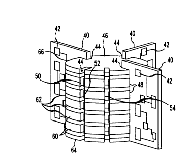
FIG. 2 illustrates the laminated cylindrical backplane with circuit cards
inserted.
Circuit cards 40 with electrical components 42 are inserted into slots 44 of
cylindrical
backplane 46. Conductive surfaces 48 positioned on the surface and near the
edge of
circuit card 40, make electrical contact with contacts 50 within slot 44 when
the edge of
the circuit card where it is inserted into slot 44.
Corresponding contacts 50 in each slot 44 are connected to form buses. For
example, contact 52 and contact 54 are electrically connected by the bus
structure of
cylindrical backplane 46. That is, similarly positioned or corresponding
contacts of a
particular layer are connected to form buses.
The laminated structure of cylindrical backplane 46 is formed with disk
sections
60 separated by dielectric layers 62. Dielectric layer 62 prevents conductive
surfaces on
the top of one disk layer 60 from short circuiting to conductive surfaces on
the lower
surface of an adjacent disk 60. Dielectric material 62 may be fabricated using
rubber or a
non-conductive plastic. Bottom layer 64 and top layer 66 provide protection
and
structural strength, and may be made of a material such as fiberglass.
Fig. 3 illustrates disk 60 that is used to form the laminated structure of
cylindrical
backplane 46. Each disk 60 contains slots adapted to receive an edge of a
circuit card.
Slots 80 are arranged along the circumference of disk 60 and may be arranged
relatively
closely together depending on the number of circuit cards required. For the
sake of
clarity, Fig. 3 shows only 4 slots. Conductive material 82 is on the top
surface of disk 60.
Conductive material 82 includes arms 84 that extend out to each of slots 80.
Each arm 84
terminates in a contact 86. On the lower surface of disk 60 (not shown in Fig.
3) is a
similar conductive material with arms that terminate in contacts 88. From the
figure it
can be seen that when circuit cards are inserted into slots 80, conductive
surfaces on one
side of the circuit card make electrical contact with contacts 86, and that
conductive
~1643~1
Siroky - 2 -
surfaces on the opposite side of the circuit card make electrical contact with
contacts 88.
As a result, all circuit card conductive surfaces that make electrical contact
with contact
86 are on a bus, where the length of that bus is equal to approximately two
times the
radius of disk 60. Similarly, all circuit card conductive surfaces that are in
electrical
contact with contact 88, are bused together by the conductive surface on the
lower surface
of disk 60.
Fig. 4 illustrates a top view of disk 60. Slots 80 are arranged along the
circumference or perimeter of disk 60, and are adapted to receive the edge of
a circuit
card. Any number of slots may be used as long as there is sufficient space so
that
adjacent circuit cards do not mechanically interfere. Disk 60 may be made of a
material
such as fiberglass.
Fig. 5 illustrates conductive material 82 that is used on the top surface of
disk 60.
Conductive material 82 may be a material such as copper that is stamped out of
a thin
sheet of copper. Conductive material 82 includes central section 100 and arms
84. The
distance from position 102 to position 104 on opposite arms should be
approximately
equal to the diameter of disk 60. End portions 106 of arms 84 are used to make
contacts
86 that were shown in Fig. 3.
Figs. 6,7 and 8 illustrate how end section 106 of arm 84 is used to form
contact
86. Fig. 6 illustrates the end portion of arm 84 including end section 106.
The first step
in forming contact 86 is to bend end section 106 downward along line 108. This
results
in the shape illustrated in Fig 7 with end section 106 at a right angle to the
remaining
portion of arm 84. Contact 86 is then formed by grasping end 110 of end
section 106 and
rolling end 110 in a counter clockwise direction to form contact 86 which is
illustrated in
Fig. 8.
Fig 9 illustrates conductive material 130 which is used on the lower surface
of
disk 60. As with conductive material 82, conductive material 130 is stamped
from a thin
conductive material such as copper. Material 130 includes center section 132
with arms
134. The distance between position 136 and 138 of opposites are should be
approximately equal to the diameter of disk 60. End sections 140 of arms 134
are used to
form contacts 88.
Figs. 10,11 and 12 illustrates how end section 140 is used to form contact 88.
Fig
illustrates a portion of arm 134 and end section 140. The first step in
forming contact
88 involves bending end section 140 in an upward direction along line 150.
This results
in the shape illustrated in Fig. 11 with end section 140 at a right angle to
the remaining
portion of arm 134. Contact 88 is then formed by grasping end 152 of end
section 140
and rotating in a clockwise direction to form contact 88 which is illustrated
in Fig. 12.
4
Siroky - 2
Fig 13 illustrates how contacts 86 and 88, formed at the ends of arms 84 and
134
respectively, align with slot 80 of disk 60. When conductive material 82 is
placed on the
top surface of disk 60 and arm 84 is positioned to lie just adjacent to slot
80, contact 86 is
positioned within slot 80 adjacent to surface 160. Similarly, when conductive
material
130 is positioned on the lower surface of disk 60 and arm 134 is positioned
just adjacent
to slot 80, contact 88 is positioned within slot 80 adjacent to surface 162.
Fig. 14 illustrates slot 80 after conductive surfaces 82 and 130 have been
applied
to the upper and lower surfaces of disk 60, respectively. As a result, it can
be seen that
contact 86 and contact 88 are now positioned in slot 80 where they can make
electrical
contact with a conductive surface near the edge of a circuit card when the
edge of the
circuit card is inserted into slot 80.
Other embodiments of the conducting surfaces may be employed. For example,
the dielectric and conductors may be formed from printed wiring board material
such as
FR4 glass epoxy with laminated and/or etched copper/tin paths. In this
embodiment,
external contacts capable of connecting the circular disks to the plugable
adapter card are
used to provide the media for continuity. The external contacts are connected
to the
internal layers using plated through hole technology while leaving the exposed
epoxy
surface to form the dielectric layer between adjacent disks. A mixture of
internal layer
and external conductive surfaces may also be used to facilitate yet another
embodiment.
The embodiment of choice depends on the bus selection and the desired physical
and
electrical attributes.
Fig. 15 illustrates laminated cylindrical backplane 46 without circuit cards
inserted into slots 80. The figure illustrates a laminated structure where
disks 60 are
separated from each other by dialectic material 62. In slots 80, contacts 86
and 88 are
visible. Contacts 86 of each disk are connected into a bus structure through
conductive
surface 82 on top of each disk 60, and contacts 88 of each disk are connected
into a bus
structure through conductive surface 130 on the lower surface of each disk 60.
Returning to Fig. 2, mounting circuit cards 40 to cylindrical backplane 46 in
an
radial form provides efficient cooling when a fan is introduced below the
cylindrical
arrangement. Cooling air is blown up through the circuit cards so that the
warm air can
rise out and away from the components on the cards. Since the cards are
arranged in a
radial fanlike orientation, adjacent slots 80 can be positioned closely
together without
overly restricting the flow of cooling air. As a result of positioning slots
80 closely
together, a large number of circuit cards can be mounted on a single
backplane. In
addition, its possible to provide electromagnetic shielding for this type of
arrangement by
21~43~1
suoky - 2
using a cylindrical metal fixture that slides over the entire arrangement
which includes
the circuit cards mounted radially to the cylindrical backplane.
The sets of contacts within the slots of the backplane may also be implemented
using one of the widely available edge connectors used in devices such as
personal
computers. In this implementation, the connectors are inserted in the slots
and the leads
on the rear of the connector are electrically connected to the appropriate
conductive
surfaces on disks 60. It is also possible to fabricate backplane 46 without
slots by
securing edge connectors to the perimeter of the backplane with the leads on
the rear of
the connector electrically connected to the appropriate conductive surfaces on
disks 60.
It is also possible to implement backplane 46 in non-cylindrical shapes. Other
shapes, such as polygons, may be used where the perimeter of the backplane
receives
circuit cards using an arrangement such as slots with contacts, slots with
connectors or
connectors secured to the perimeter of the backplane.