Note: Descriptions are shown in the official language in which they were submitted.
'- ~1~43~'~
-1_
ARTICLE COMPRISING ORGANIC THIN FILM TRANSISTORS
Field of the Invention
This invention pertains to thin film transistors (TFTs), more specifically,
to TFTs that comprise organic active layer material.
Background of the Invention
Thin film transistors ('TFTs) are known, and are of considerable
commercial significance. For instance, amorphous silicon-based TFTs are used
in a
large fraction of active matrix liquid crystal displays.
TFTs with an organic active layer are also known. See, for instance, F.
Gamier et al., Science, Vol. 265, pp. 1684-1686; H. Koezuka et al., Applied
Physics
Letters, Vol. 62 (15), pp. 1794-1796; H. Fuchigami et al., Applied Physics
Letters,
Vol. 63 (10), pp. 1372-1374; G. Horowitz et al., d. Applied Physics, Vol. 70
(1), pp.
469-475, and G. Horowitz et al., Synthetic Metals, Vol. 41-43, pp. 1127-1130.
These devices typically are field effect transistors (FETs). Such devices
potentially
have significant advantages over conventional TFTs, including a potentially
simpler
(and consequently cheaper) fabrication process, the possibility for low
temperature
processing, and compatibility with non-glass (e.g, plastic) substrates.
Bipolar
transistors that utilize both p-type and n-type organic material are also
known. See,
for instance, US patent 5,315,129. S. Miyauchi et al., Synthetic Metals, 41-43
(1991), pp. 1155-1158, disclose a junction FET that comprises a layer of p-
type
polythiophene on n-type silicon.
However, despite considerable research and development effort,
"organic" TFTs have not yet reached commercialization, at least in part due to
relatively poor device characteristics of prior art organic TFTs.
An important device characteristic of a switching transistor is the on/off
ratio of the sourceJdrain current. Prior art organic TFTs typically have
relatively low
on/off ratios. For instance, H. Fuchigami et al. (op. cit.) recently reported
a device
that had carrier mobility comparable to amorphous silicon, but had an on/off
ratio of
only about 20 at -30V gate-source voltage. That paper also discloses
purification of
semiconducting materials to reduce the carrier scattering by impurities.
H. Koezuka et al. (op. cit.) report attainment of an on/off ratio
(modulation ratio) of the channel current of about 105 in a device with doped
polypyrole-coated (a highly conducting polymer) source and drain contacts.
According to these authors, this is the highest on/off ratio achieved in
organic FETs.
Nevertheless, the reported on/off ratio is still substantially smaller than
on/off ratios
typically available in conventional FETs and demanded for many potential
CA 02164357 1999-06-04
-2-
applications of organic TFTs. Furthermore, the organic TFT had very low
carrier
mobility (2 x 10⁻⁴cm2/V~s), and thus would not have been suitable for high-
speed
operation. European patent application No. 92307470.2 (publication No. 0 528
662
A1) discloses an organic FET that comprises a first organic layer that
constitutes a
channel between source and drain electrodes and is in contact with a second
organic
layer that is disposed between the gate electrode and the source and drain
electrodes.
The first and second organic layers are of the same conductivity type but
differ in
their carrier concentration.
In view of the potential significance of organic TFTs, it would be
desirable to have available such devices that have improved characteristics,
including improved onJoff ratio of the source/drain current. This application
discloses such devices, and a method of making the devices.
U.S. Patent No. 5,693,977 issued December 2, 1997 by R.
C. Haddon et al., discloses a C ~-based organic transistor. See also A.
Dodabalapur
et al., Science, Vol. 268, p. 270 (1995).
Definitions and Glossary
An "organic semiconductor" herein is a material that contains a
substantial amount of carbon in combination with other elements, or that
comprises
an allotrope of elemental carbon (excluding diamond), and exhibits charge
carrier
mobility of at least 10-3cm2/V~s at room temperature (20°C). Organic
semiconductors of interest herein will typically have conductivity less than
about
1S/cm at 20°C.
A "p-type" ("n-type") organic semiconductor herein is an organic
semiconductor in which the Fermi energy is closer to (farther from} the energy
of the
highest occupied molecular orbital (HOMO) of the molecules or aggregates
present
in the material than it is to (from) the energy of the lowest unoccupied
molecular
orbital (LUMO). The term is also intended to mean an organic semiconductor
which
transports positive charge can~iers more (less) efficiently than negative
carriers.
Positive (negative) carriers are generally referred to as "holes"
("electrons").
An organic "p-n junction" herein is the contact region between a p-type
and a n-type organic semiconductor.
Summary of the Invention
In a broad aspect the invention is embodied in an article that comprises a
novel organic TFT that can have substantially improved characteristics (e.g.,
on/off
ratio), as compared to prior art organic TFTs. Some embodiments of the
invention
can exhibit p-channel or n-channel transistor behavior, depending on biasing
~16435'~
-3-
conditions, and need not necessarily have high on/off ratio.
Specifically, the organic TFT comprises organic material, spaced apart
first and second contact means (e.g., gold electrodes) in contact with the
organic
material, and third contact means that are spaced from each of the first and
second
contact means and that are adapted for controlling, by means of a voltage
applied to
the third contact means, a current between the first and the second contact
means.
Significantly, the organic material comprises a layer of a first organic
material of a
first conductivity type and a layer of a second organic material of a second
conductivity type that is in contact with the layer of the first organic
material at least
in a region between the first and second contact means and forms a p-n
junction with
the layer of first organic material, the layer of the first organic material
being in
contact with each of the first and second contact means and being not in
contact with
the third contact means. The third contact means generally can be identified
with the
gate contact in prior art devices, and the first and second contact means with
the
source and drain contacts of prior art devices.
Exemplarily, a TFT according to the invention has exhibited an onloff
ratio of more than 106, substantially higher than the ratios exhibited by
prior art
organic TFTs. The exemplary TFT according to the invention furthermore
exhibited
relatively high carrier mobility, in excess of 0.003 cm2 / V ~ s. Desirably,
TFTs
according to the invention exhibit an on/off ratio greater than 105 at an
operating
gate voltage, and a carrier mobility of at least 3 x 10⁻³ cm2/V~s, all at
20°C.
The layer of the first organic material in TFTs according to the invention
can comprise any of the organic materials known to be suitable for use as the
active
layer in organic TFTs. Among these materials are polythiophene and substituted
derivatives thereof such as poly(3-hexylthiophene and poly{3-octylthiophene)
polythienylenevinylene, a-hexathienylene (a-6T) and substituted derivatives
thereof
such as a, ~-dihexyl-a-6T. Other suitable first organic materials are
disclosed in US
patent 5,315,129 and in G. Horowitz et al., Synthetic Metals, Vol. 41-43, pp.
1127-
1130. Exemplarily, the first organic material is selected from polymers of
thiophene
of degree of polymerization greater than three (and typically less than 9),
polymers
of substituted derivatives of thiophene, and poly(thienylenevinylene).
Recently we
have shown that 2, 2'-bis (benzo [1,2-b: 4,5-b']dithiophene can have p-type
mobility
of > 10-4 cm2/V ~s in a TFT, with excellent on/off ratio and thermal
stability. This
compound, as well as its tris analog and substituted derivatives, is
contemplated for
use in TFTs according to the invention.
-4-
The above recited compounds are p-type organic semiconductors, but
the invention is not so limited. We currently believe that other organic
compounds
that can be deposited in thin film form and that are n-type are also likely to
be
suitable for use as the first organic material in transistors according to the
invention,
and use of these compounds is contemplated. We currently prefer first organic
semiconductor materials that can be deposited in crystalline (typically
polycrystalline) form, but amorphous layers may also have utility.
Among the second organic materials that are suitable for use in the
invention is C ~. However, the invention is not so limited, and the use of
other
organic materials, including p-type materials, is contemplated. Among n-type
organic semiconductors that are likely to be useful are other fullerines
(e.g., C ~o and
homologs), perylene tetracarbozylic anhydrides and imides and substituted
derivatives (e.g., perylene tetracarboxylic dianhydride or PTCDA), ozadiazole
compounds, tetracyanoquino-dimethanes (e.g., 7, 7, 8, 8-
tetracyanoquinodimethane
and its dibenzo derivative), porphyries and quinones. Exemplary substituents
are
nitro, cyano, halo and perHuoroalkyl substituents, with other alkyls also
being
potentially useful. Those skilled in the art will appreciate that not all n-
type organic
semiconductor materials will necessarily be useful in the practide of this
invention.
Indeed, there are materials (e.g., Alq) that are useful in some embodiments of
the
invention but are currently. not thought to be useful in other embodiments.
In a first exemplary embodiment of the invention the transistor further
comprises a dielectric layer disposed between the third contact means and both
of the
first and second contact means, with the first organic material layer in
contact with
the dielectric layer. Transistors of this embodiment have a structure
analogous to
that of conventional metal-insulator-semiconductor (MIS) FETs and will be
referred
to as organic TFfs of the MIS-FET type.
In a second exemplary embodiment the third contact means of the
transistor are disposed on the second organic material layer and are spaced
from the
first organic material layer. Transistors of this embodiment have a structure
analogous to that of conventional junction FETs (J-FETs) and will be referred
to as
organic TFTs of the J-FET type.
A third exemplary embodiment is similar to the above first embodiment,
but with the order of the first and second organic material layers
interchanged.
Transistors according to the invention are advantageously used in
articles such as display systems, memories, and other analog and/or digital
circuits.
~1643~'~
-s
A further embodiment of the invention is an organic thin film transistor
capable of operation as either a p-channel or n-channel device, and multi-
transistor
circuits that comprise such transistors. These TFTs do not necessarily possess
as
high on/off ratios as do some of the previously disclosed p-channel TFTs.
s Brief Description of the Drawings
FIG. 1 schematically shows an exemplary prior art organic TFT;
FIGs. 2-4 schematically show exemplary transistors according to the
invention;
FIGs. s and 6 show performance data of a MIS-FET-type transistor
before and after provision of a second organic material layer;
FIG. 7 shows performance data of a J-FET-type transistor according to
the invention;
FIGs. 8 and 9 schematically show the band edge alignment of isolated
a-6T and Alq, and the band edges of a-6T in contact with Alq;
is FIG. 10 shows an exemplary drive circuit in an active matrix liquid
crystal display that comprises TFTs according to the invention;
FIG. 11 schematically depicts an exemplary organic thin film transistor
capable of p-channel and n-channel operation in a single device;
FIG. 12 shows the relevant energy levels of Au, a-6T and C ~;
FIGs. 13 and 14 show energy band diagrams of the transistor according
to the invention in the p-channel and n-channel enhancement mode,
respectively;
FIGs. is and 16 show transistor characteristics for p-channel and n-
channel operation, respectively;
FIG. 17 shows further transistor characteristics; and
2s FIG. 18 schematically shows an exemplary circuit comprising n- and p-
channel transistors according to the invention.
Detailed Description
Prior art organic TFTs typically are MIS-FET-type or hybrid J-FET-type
transistors and can be embodied in a variety of structures. An exemplary prior
art
MIS-FET-type TFT (10) with organic active layer is schematically depicted in
FIG.
l, wherein numerals 11-16 refer, respectively, to the substrate (e.g., glass,
plastic,
metal, semiconductor), source electrode, drain electrode; gate electrode, gate
insulator layer and organic active material (organic semiconductor) layer. As
those
skilled in the art will appreciate, means for causing the flow of charge
carriers
3s between source and drain, and means for applying a voltage to the gate
electrode will
be present in a working device but are not shown.
-6-
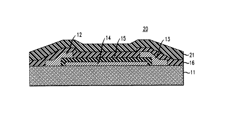
FIG. 2 schematically shows an exemplary MIS-FET-type device (20)
according to the invention. Numerals 11-16 refer to elements that respectively
correspond to elements of the same reference numeral in FIG. 1, and numeral 21
refers to an organic material layer that is of the opposite conductivity type
as layer
16, and forms a p-n junction therewith. Exemplarily, layer 16 is p-type (e.g.,
a-6T)
and layer 21 is n-type (e.g., Alq).
We have discovered that provision of an appropriate layer 21 can result
in substantially improved device performance, typically a significant decrease
in the
"off' current between source and drain, with corresponding increase in the
on/off
ratio of the transistor.
We currently believe that the decrease in the "off' current is associated
with the contact between appropriate organic layers 16 and 21, e.g., the a-
6T/Alq
interface, and attendant depletion of the (p-type) residual carriers in the
layer (e.g.,
16) of first organic material.
By analogy with conventional p-n junctions, it can be said that the width
W of the depletion layer formed at the first/second organic material interface
at zero
bias is (2E1 Vb;/qNl )u2, where el is the dielectric constant of the first
organic
material, V b; is the "built-in" potential ~ E F1 - E F2 ~ /q, N 1 i~ the free
carrier
density in the first organic material, q is the elementary charge ( 1. 6 x 10-
19 C ), and
EF1 and EF2 are the Fermi energy in the first and second organic materials,
respectively. In the above expression for W it is assumed that the second
organic
material has much higher free carrier density than the first organic material.
We currently believe that the presence of a depletion region of non-zero
width at zero bias results in lower current between the first and second
contact means
(Ip) at zero bias by causing many of the free carriers in the first organic
material
layer to be electrically inactive.
The above remarks are offered for tutorial reasons only, and are not
intended to limit the claims.
A significant feature of transistors according to the invention is a
relatively large (e.g., > O.SV) value of V b;. This in turn requires a
relatively large
difference in Fermi energy between the first and second organic materials.
This is exemplarily illustrated in FIGs. 8 and 9, which schematically
respectively show the band edge alignment of isolated a-6T and Alq, and the
band
edges of a-6T in contact with Alq. As is well known, a-6T and Alq are
recognized
as p-type and n-type organic semiconductors, respectively. The numerical
values in
FIG. 8 are in electron volts, and numerals 91-93 in FIG. 9 refer to insulator,
a-6T
_7-
and Alq, respectively.
FIGs. 5 and 6 show comparative data for a MIS-FET-type organic TFT
without and with second organic material layer, respectively. The data of FIG.
5
were obtained from a transistor of the type shown in FIG. 2, but without layer
21.
The substrate was silicon, the gate contact was a 30 nm thick gold stripe. The
gate
dielectric was a 300 nm thick layer of conventionally formed Si02. The gold
source
and drain electrodes were 30 nm thick, 250p.m long and 100p,m wide, and were
spaced apart by a distance of l2p.m. The p-type organic semiconductor layer
was 50
nm thick a-6T. The data of FIG. 6 were obtained from the above described
transistor, but with a 60 nm thick Alq layer deposited on the a-6T layer. As
can be
seen from the figures, provision of the Alq layer resulted in a significant
decrease in
drain current (Ip) at zero gate bias (V ~ = 0), exemplarily from - 1. l p.A to
-68 nA.
FIG. 7 shows similar performance data for a J-FET-type organic TFT
according to the invention. As can be seen, the device has desirably low ID at
V ~ = 0. FIG. 3 schematically depicts a J-FET-type organic TFT (30) according
to
the invention, with numerals 31-36 designating the insulating substrate, first
organic
material layer, second organic material layer, first contact means, second
contact
means, and third contact means, respectively.
FIG. 4 schematically depicts a further exemplary embodiment of the
invention that corresponds to the above described third embodiment. Numerals
41-47 refer, respectively, to the substrate, first organic semiconductor
layer, second
organic semiconductor layer, first contact, second contact, third contact, and
gate
dielectric. It will be understood that in this embodiment layer 42 is n-type
organic
semiconductor material.
The data of FIG. 7 were obtained from a TFT of the general type shown
in FIG. 3. Specifically, the substrate was Si02-coated Si. An inter-digitated
set of
source/drain electrodes ( 10 nm Cr/30 nm Au) were formed on the substrate. The
width and spacing of the fingers of the digitated structure was lOp.m; the
overall
dimensions of the structure are 2 mm x 2 mm. A 50 nm layer of a-6T was
evaporated over the interdigitated structure, and a 60 nm layer of Alq was
evaporated
onto the a-6T layer. A 100 nm thick and 3 mm wide finger of Al, defined by
means
of a shadow mask, was deposited on the Alq layer so as to extend across the
source/drain spacing. The Al finger served as the gate electrode.
Transistors according to the invention can be produced by any
appropriate method on any suitable substrate. Exemplary substrates are glass,
plastics such as MYLAR~ or KAPTON~, or Si (coated with Si02 or uncoated).
CA 02164357 1999-06-04
_g_
Although provision of a second organic material layer will generally
result in improved device characteristics if the first organic material is of
a purity
that is conventionally found in prior art devices, we have also found that, at
least in
the case of devices that comprise a-6T, the use of higher purity first organic
material
may result in additional improvement in device characteristics. Techniques for
purifying a-6T are described in co-assigned U.S. Patent No. 5,574,291 issued
November 12, 1996.
We have also found that an appropriate heat treatment of the deposited
first organic material (e.g., a-6T) can change the morphology of the layer,
and
consequently further improve device characteristics. More specifically, we
have
found that rapid thermal annealing (RTA) of deposited films of a-6T can
substantially increase the grain size of the material, to the extent that
average grain
size can exceed the channel length (typically 4- l2p.m) of the intended TFT.
If this
is the case then the active material can behave substantially like a single
crystal.
Typical as-deposited films of a-6T are polycrystalline, with average
grain size of about 100 nm or less. Annealing such films for a short time
(typically
less than 10 seconds, e.g., 1 second) at a temperature close to, the melting
point (e.g.,
295-315°C) exemplarily has resulted in increase of the average grain
size to above
2 p, m, exemplarily about 5 -100 p,m. Annealing is desirably in an inert
atmosphere,
e.g. N 2. Any suitable heat source (e.g., a bank of halogen lamps focused to a
susceptor, or a graphite strip heater) can be used.
Although in many cases the carrier mobility in the p-type material will
be substantially higher than the mobility. in the n-type material (exemplarily
by a
factor of 100 or more), it may at rimes be advantageous if the respective
mobilities in
the two materials are comparable (e.g., am within a factor of about 10 of each
other).
If this is the case then it will be possible, by appropriate biasing of the
gate electrode
in a MIS-FET type structure such as is shown in FIG. 2, to obtain either an n-
channel
or a p-channel transistor. Those skilled in the art will recognize that the
ability to
fornn either n- or p-channel transistors makes possible fabrication of
complementary
circuits, and we contemplate use of TFTs according to the invention as
building
blocks in complementary analog and/or digital circuits. Such TFTs need not
possess
very high on/off ratio in order to be useful.
Transistors according to one embodiment of the invention can be used
as discrete devices but will more typically be used in integrated circuits
that
comprise a multiplicity of transistors according to the invention, possibly in
-9-
conjunction with conventional semiconductor devices, with conductors
interconnecting the devices and providing means for energizing the devices,
providing input signals to the circuit and optionally receiving output signals
therefrom.
By way of example, transistors according to the invention are used as
current switches in liquid crystal displays in functionally the same way as
prior art
semiconductor TFTs are currently used. This is schematically illustrated in
FIG. 10,
which is based on an illustration at p. 102 of "Amorphous and Microcrystalline
Devices", J. Kanicki, editor, Artech House, Boston (1991). FIG. 10 depicts
relevant
aspects of an exemplary circuit diagram of an active-matrix liquid crystal
display,
wherein transistors 101 are TFTs according to the invention, and the remainder
of
the circuit is conventional. Numerals 102 refer to liquid crystal, and
numerals
103-105 refer to signal lines, gate lines and common electrode, respectively.
Video
signals and gate pulses are also shown schematically.
FIG. 11 schematically depicts an exemplary organic thin film transistor
according to the invention. The transistor is capable of p-channel and n-
channel
operation in a single device. Reference numerals 110-116 refer to the silicon
substrate which serves as the gate, the gate dielectric (Si02), the gate
contact (Au),
the source (Au), the drain (Au), the p-type organic layer (a-6T) and the n-
type
organic layer (C~), respectively. As those skilled in the art will recognize,
the
transistor of FIG. 11 closely resembles that of FIG. 2. As those skilled in
the art will
recognize, either or both of layers 115 and 116 can comprise more than one
organic
compound.
In a currently preferred embodiment the p-type layer consists of a-6T, is
typically about 10-20 nm thick, and is disposed on the gate dielectric. The n-
type
layer consists of C ~, is typically about 20-40 nm thick, and is disposed on
the p-
type layer. It is typically desirable to provide an electrically inactive
layer (e.g.,
Si0) on the n-type layer, to protect the n-type layer from the ambient.
It is not a requirement that the p-type material is disposed below the n-
type material. However, we have attained better device characteristics for
such
transistors, as compared to transistors having the p-type layer disposed on
the n-type
layer. Furthermore, we have observed degradation of n-channel operation if the
p-
type layer is relatively thick (typically >40nm). It thus appears desirable
that the p-
type layer is relatively thin (<40 nm, preferably <20 nm).
- ~1~43~~d
- to -
The energy levels of the highest occupied molecular orbital (HOMO)
and lowest unoccupied molecular orbitals (LUMO) a-6T and C ~ are shown in FIG.
12. As those skilled in the art will recognize, these energy levels are such
that, when
the gate is biased negatively with respect to the source, the p-channel
material (a-
6T) is filed with holes, and when the gate is biased positively with respect
to the
source, the n-channel material (C ~) is filled with electrons.
FIGs. 13 and 14 schematically show the energy band diagrams of an
exemplary transistor according to FIG. 11 in the p-channel and n-channel modes
of
operation, respectively. In the p-channel mode an accumulation layer of holes
is
formed in the a-6T near the a-6T/Si02 interface, and in the n-channel mode an
accumulation layer of electrons is formed in C ~ near the interface with a-6T.
FIGs.
13 and 14 assume an applied bias of -30 V and +60 V, respectively. Numerals
130
and 140 refer to the Fermi levels, and numeral 131 refers to the energy level
of the
metal contact.
FIGs. 15 and 16 show drain current vs. drain voltage for an exemplary
transistor according to FIG. 1 l, for p-channel and n-channel operation,
respectively.
It is to be emphasized that the data of FIGs. 15 and 16 were obtained from a
single
transistor, establishing that one and the same transistor can serve as either
a p-
channel or n-channel device. The dotted lines in FIG. 16 represent drain
currents at
low positive gate fields.
Although the discussion of complementary organic thin filin transistors
was in terms of a-6T/C~-based transistors, the invention is not so limited. We
have, for instance, achieved results qualitatively similar to those of FIGs.
15 and 16
with a transistor of the type shown in FIG. 11, but with a, w hexyl 6T
substituted for
a-6T, and we expect that many of the above recited first organic materials are
suitable for use in p- and n-channel organic thin film transistors, provided
they are
used in a combination that has an energy band line-up similar to that of the
a-6T/C~ combination of FIG. 12, and has appropriate transport properties.
Specifically, the LUMO and HOMO of the p-channel materials must be closer to
the
vacuum level than the HOMO of the n-channel material.
The data of FIGs. 15 and 16 were analyzed with a model that takes into
account short-channel effects, parasitic resistance, and field dependence of
the carrier
mobility. The p-channel mobility is about 4 x 10⁻³ cm2/V~s, and the threshold
voltage is about 0 V. The n-channel mobility is about 5 x 10⁻³ cm2/V~s, and
the
n-channel threshold voltage is about +40V. The asymmetry of device
characteristics
may be related to the fact that the HOMO energy of a-6T alinost exactly
matches the
CA 02164357 1999-06-04
-11-
work function of Au, but that the LUMO energy of C ~ matches the Au work
function only relatively poorly, with a potential barrier of >1V existing
between the
work function and the LUMO level. It is however expected that optimization of
the
contact metallizadon and device geometry will reduce both the n-channel
threshold
S voltage and the n-channel source-drain offset voltage.
Complementary circuits that utilize conventional (i.e., Si-based)
transistors are well known, and are known to be capable of operation with low
power
dissipation, see, for instance, W. N. Carr et al., "MOS/LSI Design and
Applications",
McGraw-Hill, especially pp. 77-78. In conventional complementary circuits it
is
predetermined (through choice of dopant) which transistor will be n-channel
and
which will be p-channel.
Transistors according to one embodiment of the invention can be either
p-channel or n-channel, depending on the applied bias, and thus can provide
the
circuit designer an additional degree of freedom, since a given transistor can
be a p-
1S channel device under one set of bias conditions, and a n-channel device
under
another set of bias conditions.
FIG. 18 schematically shows an exemplary complementary circuit, an
inverter, that comprises two substantially identical transistors according to
the
invention, with one of the transistors operating as an n-channel device and
the other
operating as a p-channel device.
Example: A thermally oxidized n-type Si wafer (Si0 2 thickness
-0.3p.m) was carefully cleaned in acetone and methanol, followed by a rinse in
DI
water. The Si02 was removed from predetermined portions of the wafer in
conventional manner by etching in buffered oxide etch (BOE) solution. Gold
2S contact pads were deposited on predetermined portions of both the exposed
Si and
the Si02 in conventional fashion, with the pads on the Si to function as gate
contact,
and the pads on the Si02 to function as source and drain contacts, all in a
TFT
substantially as shown in FIG. 11. Gate lengths were between l.S and 2Sp.m,
and
the pad width was 2SOp,m. The thus prepared wafer was loaded into a thermal
evaporator (base pressure < 10-6 Torr). A quantity of a-6T, prepared and
purified substantially as disclosed in U.S. Patent No. 5,574,291, was
present in the evaporator, as was a quantity of C ~, prepared substantially as
disclosed in R. C. Haddon et al., ACS Symposium Series No. 481 ( 1992), p. 71,
and
in the above cited '221 US patent application. A 1S nm film of a-6T was first
3S sublimed over the substrate, followed by sublimation of a 40 nm film of C
~, both at
~1~43~'~
- 12-
rates in the range 0.5 - 10 nm/s. Deposition of the C ~ film was followed by
sublimation of a 45 nm film of a-6T to protect the C ~ from the ambient. We
have
found that exposure to oxygen leads to degradation of transport properties in
C ~,
and may lead to such degradation also in other n-type semiconductors.
Subsequent to the deposition of the protective (electrically inactive} a-
6T film, the wafer was removed from the evaporation chamber and quickly loaded
into a vacuum probe station for transistor characterization. FTGs. 15-17 show
characteristics of a particular one of the thus produced TFTs.