Note: Descriptions are shown in the official language in which they were submitted.
2164gOl
-
Organic Chip Carriers For Wire Bond-Type Chips
Background of the Invention
1. Field of the Invention
The invention pertains generally to organic chip carriers for wire bond-type
chips .
2. Description of the Related Art
Semiconductor integrated circuit devices (hereinafter referred to as
semiconductor chips or just chips) are typically electronically packaged by
mounting one or several chips onto a ceramic , e . g ., alumina , chip carrier
substrate and using wire bonds to electrically connect I/O (input/output) contact
pads on each chip to corresponding contact pads (and therefore to corresponding
fan-out circuitry) on the ceramic chip carrier substrate. The resulting ceramic
chip carrier is then mounted onto a printed circuit board (PCB ) or printed
circuit card (PCC) and (via circuitry on the PCB or PCC) thereby electrically
connected to other such ceramic chip carriers and/or other electronic componentsmounted on the PCB or PCC.
While the above-described pa~k~ging scheme is certainly useful, the use
of ceramic chip carrier substrates does involve certain limitations and drawbacks.
For example, as is known, the speed of propagation of an electrical signal
through a wire on a dielectric layer, or between two dielectric layers, is
proportional to the inverse of the square root of the dielectric constant of thedielectric layer or layers. Unfortunately, the dielectric constants of ceramics are
relatively large, e . g., the dielectric constant of alumina is about 9, which
results in ceramic chip carriers exhibiting relatively low, and in some cases
undesirably low, signal propagation speeds.
The use of ceramic chip carrier substrates also leads to certain I/O
constraints. For example, a single-layer ceramic chip carrier substrate includesbut a single layer of fan-out circuitry on the upper surface of the single ceramic
EN9-95-004
216~901
layer, extending to contact pads around the outer periphery of the single
ceramic layer. (A lead frame, having inner leads connected to these peripheral
contact pads, is typically used to electrically connect such a ceramic chip carrier
to a PCB or PCC.) However, as the number of chip I/Os has increased, it has
been necessary to increase the number of fan-out wires, and to correspondingly
decrease the spacing between the fan-out wires, to the point where undesirable
cross-talk between adjacent fan-out wires has become unacceptable. Moreover,
it has become incre~ingly difficult, if not impossible, to form a correspondingly
large number of contact pads around the outer periphery of the ceramic layer.
Thus, single-layer ceramic chip carrier substrates are definitely limited in their
ability to handle high I / O chips .
Attempts to accomodate chips having relatively large numbers of I/Os has
led to the use of multilayer ceramic chip carrier substrates employing so-calledball grid arrays (BGAs) in lieu of lead frames. These types of ceramic chip
carrier substrates differ from single-layer ceramic chip carrier substrates in that
they include two or more layers of fan-out circuitry on two or more ceramic
layers. Significantly, these layers of fan-out circuitry are electrically
interconnected by mechanically drilled via holes, which are plated and/or filledwith electrically conductive material. In addition, a certain number of such holes
extend from the layers of fan-out circuitry to lands on the bottoms of the chip
carrier substrates, on which are mounted solder balls (formed in grid arrays,
hence the term ball grid array. ) These solder balls are intended to be
mechanically and electrically connected to corresponding solderable contact padson a PCB or PCC. Unfortunately, the mechanically drilled holes electrically
inter-connecting the layers of fan-out circuitry have relatively large diameters,
requiring the spacing between the fan-out wires to be relatively large. But, this
relatively large spacing between fan-out wires limits the number of chip I/Os
which can be accomodated by such multilayer ceramic chip carrier substrates.
Other attempts to p~ck~ge chips having a relatively large number of chip
I / Os has led to the use of multi-tiered cavities in multi-layered ceramic
substrates. (As used herein, the term "cavity" denotes a depression in a
substrate, not a hole extending through the thickness of the substrate.) When
using such a p~ck~ging configuration, a chip is mounted face-up at the bottom
of a multi-tiered cavity. Wire bonds are extended from I/O contact pads on the
EN9-95-004 2
2164901
upper surface of the chip to contact pads on each of the exposed upper surfaces
of the different layers of the multi-layered ceramic substrate constituting the
different tiers of the multi-tiered cavity. While this configuration does make it
possible to accomodate a relatively large number of chip I/Os, it does result inrelatively long wire bonds extending from the chip to the upper tiers of the
multi-tiered cavity. As a consequence, the "time of flight" of corresponding
electrical .sign~l.s is undesirably increased.
Ceramic chip carrier substrates are also limited in terms of their heat
dissipation capabilities. For example, in the case of a multilayer ceramic chip
carrier having a chip positioned at the bottom of a multi-tiered cavity, heat
dissipation is typically achieved by providing a heat sink directly beneath the
cavity. But this implies that the heat generated by the chip must necessarily beconducted through the ceramic layer at the bottom of the cavity before reaching
the heat sink. As a consequence, the rate of heat dissipation is limited.
Thus, those engaged in the development of chip carriers have sought,
thus far without success, chip carriers which: ( 1 ) exhibit relatively high
electrical signal propagation speeds; ( 2 ) accomodate relatively high I / O chips
while avoiding the need for mechanically drilled holes to interconnect differentlayers of fan-out circuitry; (3) exhibit a relatively short "time of flight"; and
(4) exhibit a relatively high rate of heat dissipation.
Summary of the Invention.
The invention involves a chip carrier which: (1) exhibits relatively high
electrical signal propagation speeds; (2) accomodates relatively high I/O chips
while avoiding the need for mechanically drilled holes to interconnect differentlayers of fan-out circuitry; (3) avoids the use of relatively long wire bonds, and
thereby achieves a relatively short "time of flight"; and (4) achieves a relatively
high rate of heat dissipation.
Significantly, the inventive chip carrier employs organic dielectric
materials, such as the epoxy/glass formulations sold under the trade names FR4.
and DriClad ., in lieu of ceramic dielectric materials. These organic materials
have relatively low dielectric constants, e.g., the dielectric constant of FR4 is
4 . 0 . As a consequence, the inventive chip carrier exhibits relatively high
EN9-95 -004 3
2164gOl
-
electrical signal propagation speeds.
The inventive chip carrier also employs an organic, photoimageable
dielectric layer which serves as a film redistribution layer (FRL). That is, this
particular organic dielectric layer is sensitive to light, and is readily selectively
exposed to light through a mask, and developed, just like a photoresist, to formvia holes (which are herein referred to as photo-vias, to distinguish them from
mechanically drilled via holes ) in the photoimageable dielectric layer .
Significantly, these photo-vias are readily formed to have diameters which are
much smaller than the diameters of vias formed using conventional mechanical
drilling techniques. For ç~ mplf~ the diameter of a conventionally drilled via hole
is typically no smaller than about 12 mils (0.012 inches), while the diameter ofa photo-via can be as small as, for example, 2 mils ( 0 . 002 inches ) .
Consequently, when such a photoimageable dielectric layer ( or layers ) is
incorporated into the inventive chip carrier, it becomes possible to interconnect
two (or more) layers of fan-out circuitry without limiting the spacing between
fan-out wires to the same degree as when using mechanically drilled vias. As a
result, the inventive chip carrier accomodates chips having a larger number of
I/Os than was possible with conventional ceramic chip carriers.
The inventive chip carrier further employs a single-tiered cavity to contain
a chip, rather than a multi-tiered cavity. As a result, relatively long wire bonds
are avoided. Consequently, the inventive chip carrier achieves a relatively
short "time of flight" for corresponding electrical F.ignAl~.
In one embodiment of the invention, thermal via holes are provided beneath
the single-tiered cavity, extending to the bottom of the chip carrier, to vent
heat produced by the chip to the atmosphere. In another embodiment, a heat
sink is provided directly beneath the thermal via holes, to further enhance heatdissipation. In still further embodiments, the chip carrier includes a metallic,e . g ., copper , layer , which acts as a heat sink , and the depth of the
single-tiered cavity extends to, or even into, the metallic layer. This results in
direct physical contact between the chip in the cavity and the heat sink, which
results in even greater heat dissipation. In yet another embodiment, the
inventive chip carrier includes at least two organic layers, with a ground planesandwiched between them. The single-tiered cavity associated with this
embodiment has a depth which extends at least to the ground plane.
EN9-95-004 4
216~901
.
Significantly, this embodiment also includes an almost continuous metal ring
which encircles the sidewalls of the cavity and extends vertically to the top
surface of the chip carrier. The presence of this metal ring is advantageous
because it permits ready electrical contact to the ground plane while avoiding the
need for a mechanically drilled via hole extending to the ground plane. As a
consequence, the spacing between fan-out wires may be advantageously reduced.
Brief Description of the Drawings
The invention is described with reference to the accompanying drawings,
wherein:
Fig. 1 is a cross-sectional view of a first embodiment of the inventive chip
carrier;
Fig. 2 is a cross-sectional view of a second embodiment of the inventive
chip carrier;
Fig. 3 is a cross-sectional view of a third embodiment of the inventive chip
carrier;
Fig. 4 is a cross-sectional view of a fourth embodiment of the inventive
chip carrier;
Fig. 5 is a cross-sectional view of a fifth embodiment of the inventive chip
carrier; and
Fig. 6 is a top view of a substrate, depicting the process used to
fabricate the fifth embodiment of the inventive chip carrier.
Detailed Description of the Preferred Embodiment(s)
The invention involves a chip carrier for wire bond-type chips which: (1)
exhibits relatively high electrical signal propagation speeds; ( 2) readily
accomodates relatively high I/O chips; (3) avoids the need for long wire bonds,
thereby achieving a relatively short "time of flight" for electrical qign~l.q
propagating through the wire bonds; and (4) achieves a relatively high rate of
heat dissipation.
As noted above, the inventive chip carrier achieves relatively high
electrical propagation speeds because it employs organic materials, such as the
EN9-95-004 5
2164901
epoxy/glass formulations sold under the trade names FR4 and DriClad, in lieu
of ceramic materials. The inventive chip carrier also readily accomodates
relatively high I/O chips because it employs at least one organic photoimageabledielectric layer in which photo-vias have been formed, as a film redistribution
layer (FRL), to electrically interconnect two (or more) layers of fan-out
circuitry. The inventive chip carrier avoids relatively long wire bonds, and thus
achieves a relatively short "time of flight" for electrical ~;ign~ propagating
through the wire bonds, because it employs a single-tiered cavity to contain a
chip, rather than a multi-tiered cavity. Further, certain embodiments of the
inventive chip carrier also include, for example, thermal vias, or a layer of
metallic material, directly beneath the chip to enhance heat transfer.
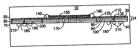
With reference now to Fig. 1, a first embodiment of the inventive chip
carrier 10 includes a chip carrier substrate 20 having opposed surfaces 30 and
40. This substrate 20 also includes a plurality , e . g ., three , of laminated ,
organic dielectric layers 50, 60 and 70 consisting of, for example, the
epoxy/glass formulations sold under the trade names FR4 and DriClad. Although
not clearly shown in Fig.1, the organic dielectric layer 50 serves to support a
layer 80 of fan-out circuitry of, for example, copper. Sandwiched between the
organic dielectric layers 50 and 60 is a layer 90 of electrically conductive
material, e.g., copper, which serves as a power plane. Sandwiched between the
organic dielectric layers 60 and 70 is another layer 100 of electrically conductive
material , e . g ., copper , which serves as a ground plane .
The thickness of each of the organic dielectric layers 50, 60 and 70 ranges
from about 2 mils to about 20 mils. Thicknesses less than about 2 mils are
undesirable because the corresponding organic dielectric layers are undesirably
flimsy, unreliable and difficult to handle. Thicknesses greater than about 20 mils
are undesirable because such thick dielectric layers are generally unnecessary
and it is difficult to drill via holes into such thick layers.
The thickness of each of the layers 80 (fan-out circuitry), 90 (power
plane) and 100 (ground plane) of electrically conductive material ranges from
about 0.125 mils to about 2.5 mils. Thicknesses less than about 0.125 mils are
undesirable because the corresponding electrically conductive layers often proveincapable of withstanding the types of temperature excursions to which the chip
carrier is likely to be subjected. Thicknesses greater than about 2.5 mils are
EN9-95-004 6
216~901
undesirable because it takes an undesirably long time to form such thick layers
using conventional plating techniques, and difficulties associated with linewidth
control are substantially increased.
As shown in Fig. 1, the chip carrier substrate 20 also includes an organic
photoimageable dielectric layer 110 which overlies the layer 80 of fan-out
circuitry . A useful composition of the layer 110 is, for example, that of the
photoimageable cationically polymerizable epoxy based material described in U.S.Patent No . 5,026,624. This particular material includes an epoxy resin system
consisting essentially of between about 10% and about 80% by weight of a polyol
resin which is a condensation product of epichlorohydrin and bisphenol A having
a molecular weight of between about 40,000 and 130,000; between about 20% and
about 90% by weight of an epoxidized octafunctional bisphenol A formaldehyde
novolac resin having a molecular weight of 4,000 to 10,000; and if flame
retardancy is required between about 35% and 50% by weight of an epoxidized
glycidyl ether of tetrabromo bisphenol A having a softening point of between
about 60C and about 11a C and a molecular weight of between about 600 and
2,500. To this resin system is added about 0.1 to about 15 parts by weight per
100 parts of resin a cationic photoinitiator capable of initiating polymerization
of said epoxidized resin system upon exposure to actinic radiation; the system
being further characterized by having an absorbance of light in the 330 to 700nmregion of less than 0.1 for a 2.0 mil thick film. Optionally, a photosensitizer
such as perylene and its derivatives or anthracene and its derivatives may be
added .
The organic photoimageable dielectric layer 110 is readily deposited using
conventional coating techniques, such as curtain coating and roll coating. The
thickness of the photoimageable dielectric layer 110 ranges from about 2 mils toabout 20 mils. Thicknesses less than about 2 mils are undesirable because it is
undesirably difficult to form such thin layers while also achieving desired
photoim~ging and dielectric properties. Thicknesses greater than about 20 mils
are undesirable because it is undesirably difficult to form small photo-vias in
such thick layers.
Using conventional photolithographic techniques, the photoimageable
dielectric layer 110 is readily selectively exposed to light through a mask, andthen developed, to form photo-vias 120 in the layer 110, as shown in Fig. 1. (It
EN9-95-004 7
2164901
:;
-
should be noted that the exposed regions undergo cross-linking, and thus
become less soluble than the unexposed regions in relation to the developer. )
These photo-vias 120 are then readily plated with an electrically conductive
material, such as copper, using conventional plating techniques.
Although not clearly shown in Fig. 1, the photoimageable dielectric layer
110 supports a layer of fan-out circuitry 130 of, for example, copper, which
includes contact pads . As should be obvious, the plated photo-vias 120 in the
photoimageable dielectric layer 110 serve to electrically interconnect the layers
130 and 80 of fan-out circuitry. Significantly, as noted above, the diameters ofthe photo-vias are smaller than the diameters of mechanically drilled via holes.Consequently, the spacing between the fan-out wires can be smaller than was
previously the case.
As shown in Fig. 1, the chip carrier substrate 20 includes a single-tiered
cavity 140, having a depth which extends only through the thickness of the
photoimageable dielectric layer 110. A wire bond-type chip 150 is positioned
face-up in the bottom of the cavity, with wire bonds 160 extending from contact
pads on the chip 150 to contact pads of the layer of fan-out circuitry 130.
Preferably , as shown in Fig . 1, the chip carrier substrate 20 includes
( mechanically drilled ) thermal via holes 170 which are positioned directly
beneath the chip 150 and extend through the thicknesses of the organic layers
80, 90 and 100. These thermal via holes 170 serve to vent the heat produced by
the chip 150 to the atmosphere, and thus serve to enhance heat dissipation. (It
should be noted that these thermal via holes are preferably filled with a
silver-filled epoxy paste to enhance heat transfer. It should also be noted thatin the final stages of fabrication, a layer of solder mask material is applied to
the surface 40 of the chip carrier 10, and thus this solder mask material overlies
the silver-filled epoxy paste.)
The diameters of the thermal via holes 170 ranges from about 6 mils to
about 12 mils. Diameters smaller than about 6 mils are undesirable because the
corresponding thermal via holes achieve undesirably little heat transfer.
Diameters greater than about 12 mils are undesirable because the layer of soldermask material in contact with the silver-filled epoxy paste in the correspondingthermal via holes tends to crack, and the overlying chip tends to d~l~min.qte
from the chip carrier substrate.
EN9-95-004 8
2164901
-
As shown in Fig. 1, the chip carrier substrate 20 further includes a
plurality of mechanically drilled, plated via holes 180. Each such hole 180
terminates at the surface 40, where it is encircled by an electrically conductive
land 190 of, for example, copper, attached to the surface 40. Also attached to
the surface 40 are a plurality of electrically conductive pads 200, as well as
electrical circuit lines (not shown) of, for example, copper, which connect the
pads 200 to plated via holes 180. Mounted on the lands 190 and pads 200 are
solder balls 210, each having a composition which includes, for example, 67% lead
and 33% tin. As should be obvious, these solder balls are to be attached to
solderable contact pads on a PCB or PCC.
With reference now to Fig. 2, a second embodiment of the chip carrier 10
differs from the first embodiment in that the depth of the single-tiered cavity
140 also extends through, for example, the organic layers 80 and 90. In
addition, a heat sink 220 is attached to the surface 40, substantially vertically
aligned with the chip 150 and the thermal via holes 170. Moreover, the solder
balls 210 are attached to lands and pads on the surface 30.
With reference now to Fig . 3, a third embodiment of the chip carrier 10
differs from the first and second embodiments in that the chip carrier substrate20 includes a relatively thick, photoimageable dielectric layer 110, immediatelyadjacent the surface 30, and a layer 230 of metallic material , e . g ., copper ,
immediately adjacent the surface 40. Here, the layer 230 acts, in part, as a
stiffener and is preferably electrically grounded. On the other hand, as before,the photoimageable dielectric layer 110 bears a layer 130 of fan-out circuitry,
including contact pads . In addition, the photoimageable dielectric layer 110
includes photo-vias 120 extending through the thickness of layer 110 to the
electrically grounded metallic layer 230. Moreover, solder balls 210 are attached
to some of the contact pads of the layer 130 of fan-out circuitry.
As shown in Fig. 3, the third embodiment of the chip carrier 10 includes
a single-tiered cavity 140 which extends through the thickness of the
photoimageable dielectric layer 110 to the layer 230 of metallic material. A wire
bond-type chip 150 sits in the bottom of the cavity 140, and is thus in direct
physical contact with the metallic layer 230. As a result, heat dissipation is
enhanced because the metallic layer 230 also acts as a heat sink.
In this third embodiment of the chip carrier 10, the thickness of the
EN9-95-004 9
216~gOl
photoimageable dielectric layer 110 ranges from about 2 mils to about 20 mils.
Thicknesses outside this range are undesirable for the reasons given above.
The thickness of the metallic layer 230 ranges from about 4 mils to about
20 mils. Thicknesses less than about 4 mils are undesirable because the
corresponding metallic layers are undesirably lacking in rigidity. Thicknesses
greater than about 20 mils are undesirable because the coefficients of thermal
expansion (CTEs) of the corresponding metallic layers then dominate the CTEs
of the corresponding chip carriers substrates, which leads to CTE mismatches
between the chip carrier substrates and the corresponding chips, which, in
turn, leads to cr~cking of the chips.
With reference now to Fig. 4, a fourth embodiment of the chip carrier 10
differs from the third embodiment in that the photoimageable dielectric layer 110
is relatively thin, and the metallic layer 230 is relatively thick. In addition, the
depth of the single-tiered cavity 140 extends through the full thickness of the
photoimageable layer 110, and partially through the thickness of the metallic
layer 230. In the fourth embodiment of the chip carrier 10, the thickness of
the photoimageable dielectric layer 110 still ranges from about 2 mils to about 20
mils. Thicknesses outside this range are undesirable for the reasons given
above .
The (full) thickness of the metallic layer 230 again ranges from about 4
mils to about 20 mils. Thicknesses outside this range are also undesirable for the
reasons given above. The (partial) thickness of the metallic layer 230
imme~ tely beneath the cavity 140 should be at least about 4 mils. Thicknesses
less than about 4 mils are llnde~irable because the corresponding metallic layers
exhibit undesirably little rigidity.
With reference now to Fig. 5, a fifth embodiment of the chip carrier 10 is
similar to the first and second embodiments in that the chip carrier substrate 20
includes a plurality , e . g ., three , of laminated organic dielectric layers 50, 60
and 70 consisting of, for example, the epoxy/glass formulation sold under the
trade name DriClad. As before, the organic dielectric layer 50 supports a layer
80 of fan-out circuitry, including contact pads. Sandwiched between the organic
dielectric layers 50 and 60 is a layer 90 of electrically conductive material, e.g.,
copper, which serves, in this embodiment, as a ground plane. Sandwiched
between the organic dielectric layers 60 and 70 is another layer 100
EN9-95-004 10
2164gOl
of electrically conductive material, e.g., copper, which serves as a power plane.
It should be noted that the ground plane extends laterally to the sidewalls of the
cavity 140, whereas the power plane does not.
The thicknesses of the organic dielectric layers 50, 60 and 70 are similar
to those given above. Also, the thicknesses of the electrically conductive layers
80 (fan-out circuitry), 90 (ground plane) and 100 (power plane) are also similarto those given above.
The fifth embodiment of the chip carrier 10 is also similar to the third and
fourth embodiments in that the chip carrier substrate 20 also includes a metallic
layer 230, which is preferably grounded. The thickness of the metallic layer 230is similar to that of the metallic layer 230 in the third embodiment.
As shown in Fig. 5, the fifth embodiment of the chip carrier 10 also
includes a single-tiered cavity 140, having a depth which extends through the
thicknesses of the organic dielectric layers 50, 60 and 70 to the metallic layer230. A chip 150 sits at the bottom of cavity 140, and is therefore in direct
physical contact with the metallic layer 230. Consequently, heat dissipation is
enhanced because, as before, the metallic layer 230 acts as a heat sink.
Significantly, the fifth embodiment of the chip carrier 10 differs from the
other embodiments in that it includes an almost continuous layer 240 of
electrically conductive material , e . g ., copper , which is attached to , and
encircles, the sidewalls of the cavity 140. This layer 240 extends vertically from
the bottom of the cavity 140 to the top of the cavity 140, and extends laterallyonto the upper surface of the organic dielectric layer 50, adjacent to the layer80 of fan-out circuitry. Because the ground plane 90 extends laterally to the
sidewalls of the cavity 140, the layer 240 is in direct physical and electrical
contact with the ground plane, and is therefore electrically grounded.
The presence of the layer 240 is advantageous because the need for a
plurality of mech~ni~lly drilled via holes ext~nt1ing through the thickness of the
organic dielectric layer 50 to the ground plane 90 is reduced. Thus, if certain
chip contact pads are to be electrically grounded, wire bonds from these chip
contact pads are extended to the portion of the layer 240 on the surface of the
organic dielectric layer 50, rather than to lands encircling mechanically drilled
via holes extending to the ground plane 90. Because relatively few such
mechanically drilled via holes are needed in the fifth embodiment, the spacing
EN9-95-004 11
218~901
-
between fan-out wires may be advantageously reduced.
It should be noted that the fifth embodiment of the chip carrier 10
includes a mechanically drilled, plated via hole 180 which extends through the
thicknesses of the organic dielectric layers 50 and 60 to the power plane 100.
Moreover, the fifth embodiment also includes a ring 250 of metal, e.g., copper,
which encircles the cavity 140 and physically and electrically contacts the plated
via hole 180 which extends to the power plane 100. This ring 250 is
advantageous because it eliminates the need for additional via holes which extend
to the power plane. Thus, electrical contact to the power plane 100 is achieved
merely by electrically contacting the ring 250.
A method for forming the layer 240 and ring 250 is depicted in Fig. 6. As
shown in Fig. 6, when forming the cavity 140, two right-angle slits 260 and 270
are mechanically cut through the thicknesses of the organic dielectric layers 50,
60 and 70. The widths of these slits ranges from about 25 mils to about 100
mils. The outer surfaces of these slits define the sidewalls of what is to be the
cavity 140. A layer of photoresist 280 is then deposited onto the surface of theorganic dielectric layer 50. This layer of photoresist is then exposed and
developed so as to leave photoresist covering all of the organic dielectric layer
50, with the exception of the slits 260 and 270, the area 241 on the surface of
the organic dielectric layer 50 to be occupied by the layer 240, and the area 251
to be occupied by the ring 250. (It should be noted that this layer of
photoresist is supported by the layers of organic dielectric material encircled by
the slits 260 and 270.) The slits 260 and 270, the area 241 to be occupied by the
layer 240, as well as the area to be occupied by the ring 250, are then
metallized using conventional seeding and metal plating techniques. Mechanical
cuts are then made through the centerlines of the slits 260 and 270, these cuts
are then extended so as to join these centerlines, and the cut-out material is
removed. This results in the formation of the cavity 140, leaving metal extending
almost continuously (with the exception of the cavity corners to which the slitsdid not originally extend) around the sidewalls of the cavity 140.
While the invention has been particularly shown and described with
reference to preferred embodiments thereof, it will be understood by those
skilled in the art that various changes in form and details may be made therein
without departing from the spirit and scope of the invention.
EN9-95-004 12