Note: Descriptions are shown in the official language in which they were submitted.
WO 95/00859 ~ ~ ' PCT/CA94/00348
1
SYSTEM AND METHOD FOR MODULATING A CARRIER
FREQUENCY
TECHNICAL FIELD
The present invention relates to a
system and method for modulating a carrier
f-.requency, and more specifically, to a Microwave
Landing System (MLS) modulated carrier frequency
generator.
BACKGROUND ART
In recent years, different techniques
for realizing a carrier frequency modulator in a
compact circuit have been developed, and
particularly for a carrier frequency modulator
working at the microwave frequency range. Among
these techniques, microwave integrated or hybrid
circuits have been proposed in the design of
microwave generators or modulators. However,
these circuits being generally expensive and
complex, there is still a need for a less
expensive circuit using simpler technology, such
as microstrip circuit manufacturing technique,
while presenting high stability and high
modulation accuracy characteristics. Moreover,
both current integrated or hybrid circuit
realizations generally require electric power
supply showing a high power output rating, due to
the high power dissipation occurring during the
operation or these circuits. Especially for
portable units operating with battery packs,
current generators or carrier frequency modulators
using integrated or hybrid circuits cannot feature
sufficient low power consumption to provide proper
power autonomy while using small battery packs,
thereby increasing physical dimensions and weight
of such portable units. This low power
consumption requirement is of a particular
WO 95/00859 PCT/CA94/00348
2
importance for portable MLS generators, which are
currently used for ramp testing of airplane
inboard MLS receivers.
SUMMARY OF INVENTION
It is thus a feature of the present
invention to provide a compact carrier frequency
modulating system featuring very low power
consumption and presenting a simple and
inexpensive design.
Another feature of the present invention
is to provide a carrier frequency modulating
system featuring high stability and high
modulation accuracy characteristics.
Another feature of the present invention
is to provide an MLS test signal generator for use
in testing MLS receivers.
Another feature of the present invention
is to provide an efficient method of modulating a
carrier frequency.
According to the above features, from a
broad aspect, the present invention provides a
carrier frequency modulating system comprising a
carrier frequency signal generator for producing a
carrier frequency signal at a carrier frequency at
an output thereof. The system further comprises a
sequences for producing a modulation signal at an
output thereof. This modulation signal comprises
a plurality of modulation signal portions
separated by at least one null modulation signal
portion having a corresponding time length. The
system is provided with a modulator for producing
a modulated carrier frequency signal at an output
thereof. The modulator has a first input
connected to the output of the carrier frequency
signal generator for receiving the carrier
frequency signal, and has a second input for
WO 95/00859 ~ ~~ ~ ~ ~ ~' ~ PCT/CA94/00348
3
receiving the modulation signal. The system
further comprises a power supply unit for
supplying electrical power to the carrier
frequency signal generator. The sequences is
' 5 connected to the carrier frequency signal
generator for controlling the activation thereof
and to interrupt the carrier frequency signal
generator rather than modulating the null
modulation signal portion during the corresponding
time length.
According to a further broad aspect of
the present invention, there is provided a method
of modulating a carrier frequency comprising the
steps of: (i) producing a carrier frequency
signal; (ii) producing a modulation signal
comprising a plurality of modulation signal
portions separated by at least one null modulation
signal portion having a corresponding time length;
(iii) modulating the carrier frequency signal
according to the plurality of modulation signal
portions; and (iv) interrupting said step (i)
instead of modulating said at least one null
modulation signal portion during said
corresponding time length.
BRIEF DESCRIPTION OF DRAWINGS
A preferred embodiment of the present
invention will now be described with reference to
the accompanying drawings in which:
FIGURE 1 is a schematic view showing
various positions of an
airplane with reference to an
MLS scanning beam.
FIGURE 2 is a diagram showing a single
MLS function comprising a
phase modulation data portion
followed by an amplitude
WO 95/00859 ~ ~ ~ ~ PCT/CA94/00348
4
modulation MLS angle
information portion.
FIGURE 3 is a diagram showing the '
envelope of a typical MLS
phase modulated carrier
frequency signal produced by
an MLS generator as provided
by the present invention.
FIGURE 4 is a general block diagram of
the carrier frequency
modulator as provided by the
present invention.
FIGURE 5A is a diagram showing waveform
of a multiplier control
signal produced by a
sequencer as provided by this
invention.
FIGURE 5B is a diagram showing waveform
of a harmonics generator
control signal produced by
the sequencer as provided by
this invention.
FIGURE 5C is a diagram showing waveform
of a modulation signal
produced by the sequencer as
provided by this invention.
FIGURE 5D is a diagram showing waveform
of a carrier frequency signal
level control signal produced
by the sequencer as provided
by this invention.
FIGURE 6A is an electronic drawing of
the generator according to
the present invention.
FIGURE 6B is a block diagram of the
carrier frequency modulator
WO 95/00859 ~ ~ PCT/CA94/00348
section according to this
invention.
FIGURE 7 is a physical representation
of the microstrip realization
5 of the carrier frequency
generator and carrier
frequency modulator according
to the present invention.
FIGURE 8 is a schematic diagram of the
sequencer as proposed by the
present invention.
FIGURE 9A is a schematic diagram of a
function address generator
memory provided in the
sequencer of the present
invention.
FIGURE 9B is a schematic diagram of a
function memory provided in
the sequencer of the present
invention.
FIGURE 10 is a block diagram showing a
particular digital to analog
converter according to
another example of a method
for producing an amplitude
modulation signal according
to the present invention.
FIGURE 11 to 14 are diagrams
representing amplitude
variation curves with respect
to time for various signals
produced by the digital to
analog converter as shown in
FIGURE 10.
PCT/CA94100348
WO 95/00859 ~~
6
DESCRIPTION OF PREFERRED EMBODIMENTS
Referring to figure.l, there are shown '
three different positions A, B and C of an
airplane 10 intersected by an MLS scanning beam
11, with reference to ~an MLS azimuth scanning
range measured in degrees on the axis 12, and to
time on axis 13. As well known in the art, second
and third scanning ranges can be provided,
respectively associated with elevation and back
azimuth data. A TO beam scan line 8, and a FROM
beam scan line 9 delimit time separations in
microseconds between TO and FROM beam centers. In
an example as shown in FIGURE 1, time separations
tA, tg and tC respectively correspond to airplane
positions A, B and C. According to the following
well-known relation:
(TO - t ) V/2
Wherein:
~ is the azimuth or elevation guidance
angle in degrees;
t is the time separation in microseconds
between TO and FROM beam centers;
TO is the time separation in
microseconds between TO and FROM beam centers
corresponding to zero degree;
V is the scan velocity scaling constant
in degrees per microsecond;
it is therefore possible to derive the accurate
position of the airplane 10 with reference to the
zero degrees axis 15, as can be also seen with
reference to FIGURE 2, which shows a single MLS
angle function comprising phase modulated data ,
portions 14 and 16, which are followed by an
amplitude modulated angle information portion
generally designated at numeral 17. As shown in
WO 95/00859 ~ ~ PCT/CA94/00348
7
FIGURE 2, amplitude level of an MLS phase
modulated data signal portion is typically about -
40dBm. The first phase modulated data portion 14
is a preamble data portion comprising MLS function
identification data, and defines a reference time
25. The second phase modulated data portion 16
comprises data for scanning sector signals
generation. The function is then comprised by a TO
scan time slot 19 and a FROM scan time slot 21,
which are separated by a pause time 23. At a
predetermined time position in the TO scan time
slot, which depends on the position of the
airplane 10 in the scanning range as shown in
FIGURE 1, a TO pulse 27 is generated, which
corresponds to the intersection of a TO beam
moving through the scanning range toward the
airplane position. During the pause time slot 23,
the beam moving away from the airplane reaches a
mid scan point 29, which corresponds to the return
of-_ the scanning beam back toward the airplane
position. The starting point of a mid scan time
separation TM corresponds to reference time 25. A
FROM pulse 31 is then generated, which corresponds
to the intersection of a FROM beam moving through
the scanning range back to the airplane position.
As shown in FIGURE 2, amplitude level of an MLS
amplitude modulation data signal portion is
typically about -34dBm.
It is pointed out that beam scanning
speed is chosen sufficiently high compared to
maximum airplane landing speed to render variation
of airplane position during time separation t
between TO and FROM pulses negligible. FIGURE 2
also shows time separation TO between TO and FROM
beam centers corresponding to zero degree
direction, as designated at position B in FIGURE
WO 95/00859 PCT/CA94/00348
8
1. Following the FROM pulse 31, an end of
function data portion 33 a.s finally generated.
Other MLS angle functions can be successively
generated similarly as hereabove described, which
typically have time lengths varying from 3.1 '
milliseconds to 15.9 milliseconds in an MLS
application as provided in a proposed example of
the present invention. Furthermore, series of
transmitted MLS angle functions can be interleaved
with basic or auxiliary data functions giving
essential or complementary information which will
be subsequently used at the receiver station to
derive angle parameters, airplane and landing
strip parameters and environmental data. For
instance, basic data could consist of scanning
range width, landing strip orientation with
reference to north, etc., and auxiliary data could
provide the ground antenna alignment information.
The system as hereunder described is an MLS
function generator and carrier frequency modulator
which can test an airplane MLS receiver while the
airplane is on its ramp, by simulating phase
modulated data and amplitude modulated angle
information of a transmitted MLS signal, as if it
was produced by an MLS ground scanning generator
in the direction of an airplane in flight before
landing.
In FIGURE 3 there is shown a typical MLS
phase modulated carrier frequency signal
transmitting coded data on a test channel
according to the first phase modulation data
sections 14 and 16 of the MLS function as shown in
FIGURE 2. In the example shown, the waveform
envelope, generally designated at numeral 37,
comprises a succession of high and low states 39
and 41, the time lengths of which being
CA 02165420 2003-O1-15
9
respectively delimited by 90 .percent amplitude
points 43, 45 and 47. In a particular example as
shown in FIGURE 3, the phase modulation is carried
out by. varying the high state time length between
a given minimum value to a maximum value of 54
microseconds, and by varying correspondingly the
low state time lel~gth between a minimum value of
microseconds and a given value depending on
high state time length, whereby the cumulative
IO time length of two successive high and low states
always totals 64 microseconds, corresponding to a
complete cycle as designated at numeral 53.
Obviously, other values of high and low states
time lengths could be proposed, depending upon the
application. .
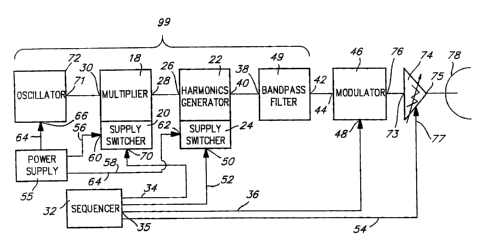
Referring now to FIGURE 4, the carrier
frequency modulator as proposed by the present
invention comprises a carrier frequency generator
99 basically consisting of an oscillator 72, a
multiplier 18 having a supply switcher 20, and a
harmonics generator 22 having a supply switcher
24. A power supply_ unit 55 supplies electrical
power to the multiplier 18 and to the harmonics
generator 22 respectively through lines 56 and 58
and supply switchers inputs 60 and 62. The
harmonics generator 22 has an input 26 connected
to an output 28 provided on the multiplier 18.
The multiplier l8 receives from the output 71 of
the oscillator 72, which is fed by electrical
power from the power supply 55 through line 64 and
oscillator input 66, a first signal at a first
frequency at an input 30 thereof, and sends to the
harmonics generator 22 a signal having a second
frequency, which is higher than the frequency of
the first signal. ~In a preferred embodiment of
the present invention, the oscillator 72 is a
CA 02165420 2003-O1-15
temperature compensated crystal oscillator (TCXO)
producing a sinusoidal waveform signal at a first
frequency of 43 MHz. The multiplier 18 can be
comprised by a pair of triplers connected in
5 series; the combination thereof providing a
frequency multiplying factor of -9, thereby
producing a sinusoidal waveform signal at a second
frequency of 387 MHz. Each tripler could be
designed with an amplifier (not shown) used in
l0 discontinuous mode followed by bandpass filters
(not shown), as well known in the art.
Alternatively, the multiplier 18 can be realized
with a phase lock loop circuit configuration (.not
shown), as also, well known in the art, the locking
time of the oscillator being a critical factor in
such a design. Moreover, the multiplier can be
omitted through the use as oscillator 72, of a
very high frequency TCXO directly supplying the
desired sinusoidal waveform signal at 38.7 MHz.
The harmonics generator 22 then produces
at an output 40 thereof higher harmonic
frequencies of the second 387 MHz frequency. The
carrier frequency generator 99 further comprises a
bandpass filter 49 having an input 38 connected to
the output 40 of the harmonic generator, to select
a substantially narrow.frequency band centered at
a preselected single harmonic frequency from
harmonic frequencies produced by harmonics
generator 22; thereby producing a corresponding
carrier frequency signal at a carrier frequency at
an output 42 provided onsaid carrier frequency
generator 99 : which is then directed toward an
input 44 of a carrier frequency modulator 46,
which will be described- later in more detail _ In
a preferred embodiment of the present invention,
the 13th harmonic frequency is selected, which
WO 95/00859' PCT/CA94/00348
11
another harmonic frequency can be selected,
depending on the desired carrier frequency_ The
system is further provided with a sequencer 32,
which produces a modulation signal at an output 35
S thereof. According to the example as shown in
FIGURE 4, the sequencer 32 could be provided with
an integrated oscillator producing a required
clock reference signal. Alternatively, the
s~equencer 32 could be connected to the output 71
of oscillator 72 to provide the sequencer 32 with
a clock reference signal (not shown). A
modulation signal is fed to input 48 provided on
the modulator 46 through a line 36. Referring to
FIGURE 5C, there is shown an example of such a
modulation signal, which comprises a plurality of
modulation signal portions 68 and 68', which are
separated by at least one null modulation signal
portion 69 having a corresponding time length.
The modulation signal portion 68 is used to
produce correspondent phase modulated data
portions 14 and 16 as illustrated on FIGURE 2, and
modulation signal portion 68' is used to produce
correspondent amplitude modulated angle
information portion generally designated at 17 in
FIGURE 2.
Returning to FIGURE 4, the sequencer 32
sends a multiplier control signal to an input 70
of the supply switcher 20 of multiplier 18 through
a line 34. In an embodiment of the present
invention where the multiplier is omitted by
employing a very high frequency TCXO as oscillator
72, the line 34 of sequencer 24 should be
connected therewith for transmitting an oscillator
control signal to an input of a supply switcher
(not shown) coupled to or integrated into the
TCXO. Referring to FIGURE 5A, there is shown an
WO 95/00859 ~ ~ ~ ~ PCT/CA94/00348
i
12
example of a multiplier control signal comprising
successive high and low signal levels, which
correspond respectively to "on" and "off°' control
states for the supply switcher 20 of the
multiplier 18. Returning to FIGURE ~4, the
sequencer 32 further sends a harmonicsgenerator
control signal to an input 50 of the supply
switcher 24 of harmonics generator 22 through a
line 52. Referring to FIGURE 5B, there is shown
an example of a multiplier control signal
comprising successive high and low signal levels,
which corresponds respectively to "on" and "off"
control states for the supply switcher 24 of the
harmonics generator 22. The sequencer 32
successively switches supply switchers 20 and 24
for controlling respectively the activation of
multiplier 18 and harmonics generator 22 whereby
to interrupt multiplier 18 and harmonics generator
22 instead of modulating the null modulation
signal portion 69 during a corresponding time
length, as shown in FIGURE 5C. Returning to
FIGURE 4, a variable attenuator 74 is provided for
receiving at a first input 73 the modulated
carrier frequency signal produced at the output 76
of modulator 46, and for adjusting the output
level of the modulated carrier frequency signal at
a desired level. Referring to FIGURE 5D, there is
shown an example of a carrier frequency signal
level control signal having variable amplitude
discretely varying in two or more steps from a
given minimum value to a given maximum value. The
variable attenuator 74 has a modulated carrier
frequency signal output 75 which is connected to a
parabolic antenna 78 for transmitting to a
receiver (not shown). For carrier frequency
modulating applications other than MLS, the
WO 95/00859 ~ PCT/CA94/00348
13
modulated carrier frequency output signal could be
transmitted to a receiver through a cable line.
Now the sequence of production of the modulation
and controls signals by the sequencer 32 will be
' 5 explained with reference to FIGURES 5A, 5B, 5C and
5D. At the beginning of a function transmission
sequence, the multiplier control signal is set to
the "on" control state at a time T1 as shown in
FIGURE 5A to switch on the supply switcher 20
l0 causing the activation of the multiplier 18. The
harmonics generator control signal is then set to
the "on" state at a time T2 as shown in FIGURE 5B
to switch on the supply switcher 24 causing the
activation of the harmonics generator 22. The
15 modulation signal is simultaneously set at a
maximum value, which signal, shown in FIGURE 5C,
is fed to the modulator 46, as shown in FIGURE 4.
The transmission of digital phase modulation data
comprised in the modulation signal then starts at
20 a time T3, or could be preceded by a number of
controls data bits for controlling the operation
of the digital to analog converter 161, for both
phase or amplitude modulation, as will be later
explained in more detail with reference to FIGURES
25 8 and 10. After transmission of the phase
modulating data, multiplier and harmonics
generator control signals are simultaneously set
to the "off" state at a time T4, thereby
minimizing power consumption of the system. At a
30 following time T5, the modulation signal is set to
. a null value corresponding to the beginning of the
null modulation signal portion 69. A relatively
short period of time before the end of the time
length of the null modulation signal portion, at
35 time T6 as shown in FIGURE 5A, the multiplier
control signal is again set to the "on" state,
WO 95/00859 PCT/CA94/00348
14
simultaneously with the activation of the
production of the carrier frequency signal level
control signal which is set to a given amplitude '
value between a minimum and a~maximum value, as
shown in FIGURE 5D. Theharmonics generator '
control signal is then again set to the "on" state
at a time T7 as shown in FIGURE 5B, just before
the beginning to the transmission of the amplitude
modulation signal portion 68' occurring at time
T8, as shown in FIGURE 5C. Following function
modulation signals can be transmitted in a same
manner as hereabove explained.
Referring now to FIGURES 6A and 7,
details on the carrier frequency generator and
carrier frequency modulator are presented. The
second frequency produced at the output of the
multiplier, which second frequency is 387 MHz in a
particular example shown, is fed at the input 26
to a coupling capacitor 80 through a line 82,
which directs the resulting signal to an input 83
of a clipping amplifier 84, which provides a
second frequency signal having a stable and
sufficient power output level. The harmonics
generator control signal from the supply switcher
24 is fed to an input 86 of a coupling circuit
which comprises a resistor 88 at the output of
which are connected in parallel a grounded
capacitor 90 and an inductance 92 feeding a proper
harmonics generator control signal to the input 93
of an impedance matching circuit 94, which
comprises a coupling capacitor to the output of
which are first connected in parallel a resistor
96 and a first grounded capacitor 98 and secondly
connected in series a first inductance 100. An
output of inductance 100 is first connected to a
second capacitor 101 and secondly connected to a
WO 95/00859 ~ ~ PCTICA94100348
second inductance 102 having an output 103
connected to an output 104 of the impedance
matching circuit 94. The output 104 is connected
to the negative terminal 106 of a step recovery
' S diode 108, whereby the impedance matching circuit
94 provides maximum energy transfer between
clipping amplifier 84 and step recovery diode 108.
Whenever the step recovery diode is polarized in
an inverted conduction state by the second
10 frequency signal coming from multiplier 18, very
short duration series of pulses are produced at
the terminal 106 of the step recovery diode, which
series correspond to a plurality of rates
associated with harmonic frequencies of the basic
15 second frequency. The pulses of a given series
have time lengths substantially equal to half the
period of the corresponding desired harmonic
frequency. The pulses are then prefiltered by a
quarter of wavelength bandpass filter 110 tuned at
the desired harmonic carrier frequency, which is
followed by a coupling capacitor in series with an
attenuator 114 for impedance matching purposes
with a following carrier frequency modulator
section of the circuit, as shown in FIGURES 6B and
7. A bandpass filter section 49 comprises a
bandpass filter 118 and a lowpass filter 124. The
bandpass filter 118 selects a substantially narrow
frequency band centered at a single harmonic
frequency from harmonic frequencies of the pulsed
signal as produced at the output 40 of attenuator
114. In a preferred embodiment of the present
invention, the 13th harmonic of the pulsed signal
is selected by the filter 118, which is a 4th
order Chebychev bandpass filter comprising a
series of coupled resonating parallel transmission
lines 119, 120, 121, 122, and 123, in an example
WO 95/00859' ~ ~ ~ ~ ~ PCT/CA94/00348
16
as shown in FIGURE 7. . The bandwidth of the
bandpass filter 118 is 'compatible with harmonic
frequencies separation and with filter temperature
stability as required by the system. The produced
filtered pulsed signal is then fed to a lowpass '
filter 124, as shown in FIGURES 6B and 7, which
has a cutoff frequency higher than the selected
single harmonic frequency and being in a range
near thereto, whereby to produce, at an output 42,
a carrier frequency signal substantially free of
interference harmonic frequencies generated by the
bandpass filter 118. A modulator 46 has a first
input 44 for receiving the carrier frequency
signal, and a second input 48 for receiving phase
and amplitude modulation signals coming from the
sequencer through the line 36 as better shown in
FIGURE 4. Carrier frequency decoupling devices
134 are connected to the line 36 ahead of input
48, for preventing the carrier frequency signal
from reaching sequencer through the line 36 (see
FIGURE 7). A preferred embodiment of the present
invention provides a modulator 46 comprising a
"rat race" type phase modulating circuit having a
first connecting node 126 connecting the carrier
frequency signal input 44 to respective inputs 127
and 128 of first and second conducting paths 129
and 130 having a difference in length
substantially equal to half a wavelength
corresponding to the carrier signal frequency.
Conducting paths 129 and 130 have respective
outputs 132 and 133 being connected to the output
of the modulator 46 at a second connecting node
135. The modulator further comprises a switching
device 131 connected to the modulation signal
input 48, and connected to the conducting paths
129 and 130 to successively activate only one
WO 95/00859 PCT/CA94/00348
17
conducting path at a time, whereby to produce, by
switching between a positive maximum amplitude and
a negative maximum amplitude, the phase modulated
carrier frequency portion of the modulated carrier
frequency characterized by a required 180 degrees
shift provided by the half a wavelength paths
difference, and to produce in a single polarity
mode the amplitude carrier frequency portion of
the modulated carrier frequency. In an example of
the present invention as shown in FIGURE 7, the
modulator 46 is a phase shift keying (PSK)
modulator designed and properly fed to provide a
DPSK (differential phase shift keying) modulation
as required by an MLS receiver system. However,
it is within the ambit of the present invention to
provide other types of modulation as PSK, QPSK,
BPSK, M-PSK, FM or FSK, implying the use of proper
carrier frequency modulator circuits which can be
readily proposed by a person skilled in the art.
For the carrier frequency amplitude modulation,
the amplitude of the modulation carrier frequency
signal is varied between a substantially null
value and a maximum value, for either a positive
or negative polarity. For a null modulation
amplitude signal value, both paths 129 and 130 are
open, and a substantially null output signal is
obtained (about -20 dBm) using a properly balanced
modulator, since signals propagating on respective
paths 129 and 130 are mutually cancelled. Each of
conducting paths 129 and 130 comprises first and
second portions 136, 137 and 136' 137' connected
respectively by third and fourth nodes 138 and 139
. which are spaced from the first node 126 by a
distance substantially equal to half a wavelength
corresponding to the carrier frequency. The
second portion 137 of the first conducting path
~v~~ ~~~
WO 95/00859 PCq'/CA94/00348
18
129 has a length separating the third node 138
from the second node-. 135 by a distance
substantially equal to three quarter a wavelength
corresponding to the carrier frequency. The
second portion 137' of the second conducting path
130 has a length separating the fourth node 139
from the second node 135 by a distance
substantially equal to half a wavelength
corresponding to the carrier frequency. In this
way, the required half a wavelength difference in
length between conducting paths is provided. The
switching device 131 is connected to the first and
the second conducting paths respectively at third
and fourth nodes 138 and 139. The switching
device 131 comprises first and second diodes 140
and 141 having opposed polarity terminals 143 and
145 being connected to the input 48 for receiving
the modulation signal, and being connected to a
ground 142 of the system. Each terminal of a
second pair of opposed polarity terminals 146 and
148 are respectively connected to the third and
fourth connecting nodes 138 and 139. In this way,
the carrier frequency signal traverses the first
conducting path 129 whenever second diode 141 is
caused to conduct by the modulation signal, and
the carrier frequency signal traverses the second
conducting path 130 whenever the first diode 140
is caused to conduct by the modulation signal.
For the carrier frequency amplitude modulation, it
is pointed out that having the response curve of
the modulator 46 characterizing the output power
thereof in terms of amplitude, a desired pulse
waveform can be produced by selecting appropriate
amplitudes, and knowing the temperature behavior
of diodes, the sequencer can be programmed to vary
the amplitude of said amplitude modulation signal
WO 95/00859 PCT/CA94/00348
19
in successive increasing or decreasing
predetermined steps separated by predetermined
time periods, as illustrated in FIGURE 5C with
reference to time periods t1, t2, t3, etc.
respectively corresponding to amplitudes al, a2,
a3, etc. Since the harmonics generator control
signal is set to the "on" state at a time T7 just
before the beginning to the transmission of the
amplitude modulation signal portion 68' occurring
at time T8, as earlier explained with reference to
FIGURES 5B and 5C, it is possible to produce a
first main basic amplitude portion on which either
amplitude portions al, a2, a3, etc. are added to
produce the required amplitude modulation signal.
Temperature compensation of the modulator 46 is
carried out by controlling current circulating in
diodes 140 and 141 with a temperature sensitive
tlzermistor circuit (not shown). The modulated
carrier frequency signal produced at an output 76
of the modulator 46 is directed to an optional
second bandpass filter 150 acting as a dual band
rejector, to attenuate frequencies adjacent the
carrier frequency. The resulting single frequency
modulated carrier frequency signal is then
directed to the input 73 of a variable attenuator
74, through a coupling capacitor 152, the variable
attenuator 74 receiving at a second input 77 a
carrier frequency signal level control signal from
the sequencer through a line 54, as earlier
explained with reference to FIGURE 4. Such a
variable attenuator can be realized using diodes
switching between a direct path and an attenuated
path whose attenuation can be adjusted to one of
predetermined levels. Alternatively, a variable
attenuator can be realized using FET transistors
mounted in a T or ~r configuration, on which a gate
CA 02165420 2003-03-25
modulated voltage is applied to obtain the desired
attenuation level. The filtered modulated carrier
frequency signal produced at the variable
atthanuator output 75 is connected to. a parabolic
5 antenna 78 as shown i~x FIGURE 68, for transmitting
to a receiver (not shown). Finally, a tunable
impedance matching line l54 is connected to the
terminal of the antenna 78, v~rhich matching line
has a length corresponding to approximately half a
10 wavelength of the carrier frequency.
Referring now to FIGURE 8, an example of
a sequences according to the present invention is
illustrated, wherein this sequences comprises a
digital generator, generally designated at numeral
i5- 15fi, for producing a. digital modulation signal
through a hne 158, control signals for ,the
carrier frequency signal generator ,99 through
lines. 34 and 52, and carrier frequency signal
level digital .acntrol signal through a line 160.
The sequences is further provided with a first
digital ;to analog converter 161 to produce a
corresponding analog modulation signal at an
output 35, which .signal is directed toward the
modulator input 48 through . the line 36; as better
shown in FIGURE 4. When a stepped amplitude
modulation signal as earlier described in
reference with Figure 5C is wanted, the.digital to
analog converter 161 produces an analog signal
showing successive amplitude levels as coded in
groups of data bits contained in function
elements, as will be later explained.
Turning now to FIGURE 10, there is
illustrated a particular digital to analog
converter which can be usedw fox carrying out
33 another method for producing the amplitude
modulation portion of the modulation signal
WO 95/00859 PCT/CA94/00348
21
according to the present invention, which method
consists in applying a variable slope delta
modulation technique. This particular device can
be connected. in the same way as the digital to
s analog converter 161 as shown in FIGURE 8.
Referring to graph A of FIGURE 14, there is
graphically represented an approximation of a
desired modulation signal waveform envelope, which
signal after proper lowpass filtering and voltage
to current converting, is fed to the modulator, as
earlier explained with reference to FIGURE 4. In
a particular instance as shown in graph A of
FIGURE 14, the waveform has been chosen in such a
manner to obtain, after lowpass filtering and
modulation, an amplitude modulated signal which is
a fair approximation of a real MLS amplitude
modulated signal, as shown in FIGURE 2.
Therefore, in predetermining the waveform
characteristics through proper sequencer encoding,
one should consider transfer functions of lowpass
filter and modulator section.
Turning now to FIGURE 10, a first bit Bi
of a properly encoded serial digital bits string
signal, coming from the sequencer driver 216 as
shown in FIGURE 8, is fed to an input 260 of a
decoder/controller 261, which has a second input
262 for receiving a reference clock signal, as
shown in graph E of FIGURE 14, from a reference
clock 264 through a line 263, which reference
clock 264 is preferably synchronized with the
reference clock signal generator 248 as shown in
FIGURE 8. The decoder/controller receives and
decodes the control data bits provided
simultaneously with the modulation data bits, as
earlier described with reference to FIGURE 5C, to
produce at a second output 266 thereof a
PCT/CA94/00348
WO 95/008.~~
22
corresponding control signal transmitted to a
control input 267 of a port selector 268 through a
line 269. In the example as shown in FIGURE 10,
the control data bits code indicates to the
decoder/controller 261 the kind of modulation
characterizing the incoming modulation bits
string, either phase modulation or amplitude
modulation. Whenever a phase modulation code is
detected by the decoder/controller 261, the latter
i0 sends a control signal to the port selector 268
through the line 269, which causes the selector to
connect an output 271 thereof with a first port
272 thereof. The decoder/controller 261 then
produces at a third output 270 thereof a phase
modulation signal Vb whose amplitude should take
one of two amplitudes values, say +V3 or
-V3, as shown in FIGURE 12, which shows only two
cycles comprised in the modulation signal portion
of a modulation signal as shown in FIGURE 5C.
This phase modulation signal Vb is fed to an input
273 of a second lowpass filter 274, which extends
rise and fall times of the incoming phase
modulation signal Vb to produce a filtered phase
modulation signal Vd at an output 276 thereof,
which signal has a waveform as shown in FIGURE 13.
This signal then exits the selector 268 through
its output 271. Whenever an amplitude modulation
code is detected by the decoder/controller, the
latter sends a,control signal to the port selector
268 through the line 269, which causes the
selector to connect its output 271 with a second
port 278 thereof. At a following clock pulse the
value of a first modulation data bit Bi of the _
amplitude modulation bits string is stored in a
first memory cell 280 of a shift register 282
provided in the detector/controller 261,
~1654~Q
WO 95/00859 PCTlCA94/00348
23
associating this value to a first shift register
bit B0, immediately after a current prior value of
B0 has been transferred to a second memory cell
284, associating this value to a second shift
register bit Bl. Therefore, the value previously
stored in the memory cell 284 is lost, being
replaced by the prior value of B0. Such a process
is successively repeated, until the last bit of
t:he transmitted modulation bits string is stored
in the shift register. An example of two bits
sequential coding will be hereunder explained with
reference to the following TABLE I:
BO B1 Polarity Slope
Amplitude
0 0 - A1
1 0 -~' Al
1 1 + A2
0 1 - A2
TABLE I gives sampled pairs of bits
values which are chosen to correspond respectively
to the different control states characterized by
a given polarity (+ or -) and a given slope
amplitude value selected from two predetermined
amplitude values in an example using two bits
cading. Obviously, in order to build a desired
waveform with more accuracy, more than two
predetermined amplitude values could be selected,
by using three or more bits for the sample coding.
Conversely, one can propose to use a single bit
sample coding in such cases when a single slope
amplitude value yields acceptable results.
Returning to FIGURE 10, it is pointed out that
depending upon the values of the sampled pair of
bits B0 and Bl as currently stored in shift
register memory cells 280 and 284, the logic
decoder/controller produces a pre integration
WO 95/00859 PCT/CA94/00348
24
signal V~ characterizing the current polarity and
slope values as determined by current BO and B1
values, the signal Va having an amplitude which
should take one of four amplitudes values, say
+V2, +V1, -V1 or -V2, as shown in FIGURE 11. The '
pre integration signal Va is sent through a first
output 286 provided on the decoder/controller 261
to an input 288 of a limner integrator 290 having
an output 292 through which an output signal Va is
produced and sent to the second port 278 of the
selector 268, which signal Va then exits the
selector 268 through its output 271. The signal
Va waveform is illustrated on graph A of FIGURE
14, which shows an approximation of a desired
modulation signal waveform envelope. Operation
details of the limiter integrator 290 digital to
analog converter as shown in FIGURE 10 will be now
explained with reference to FIGURE 14 and TABLE I.
Prior to the transmission of a bits string
corresponding to a given amplitude modulation
portion, the values of BO and Bl are both
initially set to "0" values, the
decoder/controller 261 accordingly sending to the
limiter/integrator 290 a pre integration signal Va
showing negative polarity and a V1 amplitude
value, which corresponds to a "-A1" slope
amplitude, according to the predetermined values
given in TABLE I. As shown in graph A of FIGURE
14, the initial waveform amplitude value of the
signal Va at the output 292 of the limiter
integrator 290 is set to zero, and since the
integration provided thereby is limited to
positive range in a such way that Va is always
equal to or greater than zero, the output signal
at 292 is kept constant to a zero value. At time
t0, a first bit Bi of the phase modulation data
WO 95/00859 PCT/CA94/00348
bits string having a "0" value is fed to the
decoder/controller 261 and the reference clock 264
simultaneously sends a clock signal to the shift
register of the decoder/controller for triggering
5 the transfer a "0" value stored in the memory cell
280 into memory cell 284 and storing the
corresponding "0" value in the memory cell 280 as
B0. Since the values of BO and Bl are still set
t o "0", the limiter integrator output signal Va is
10 accordingly kept to a zero value, as shown at
numeral 294. At time t1, the resulting values of
BO and B1 remain unchanged, and the limiter
integrator output signal Va is still kept to a
zero value, as shown at numeral 296. At time t2,
15 a following bit Bi having a "1" value is fed to
the input 260 of the decoder/controller and the
reference clock 264 simultaneously sends a clock
signal to the shift register of the
decoder/controller for triggering the transfer of
20 a "0" value stored in the memory cell 280 into
memory cell 284 and storing the corresponding "1"
value in the memory cell 280 as the current value
of B0. Then, the decoder/controller 261
accordingly sends to the limiter/integrator 290 a
25 pre integration signal Va showing positive
polarity and V1 amplitude value, which corresponds
to a "+A1" slope amplitude, according to the
predetermined values given in TABLE I. As shown
at numeral 298 in graph A of FIGURE 14, the
limiter integrator begins to produce an integrated
linear waveform amplitude signal characterized by
a first slope. At time t3, a following bit Bi of
the phase modulation data bits string having a "1"
value is fed to the decoder/controller 261 and the
reference clock 264 simultaneously sends a clock
signal to the shift register of the
WO 9S/00859 PCT/C.~94/00348
26
decoder/controller of the decoder/controller for
triggering the transfer of a "1" value stored in
the memory cell 280 into the memory cell 284 and
storing the corresponding "1" value in the memory
cell 280 as the current value of B0. Then, the
decoder/controller 261 accordingly sends to the
limiter/integrator 290 a pre integration signal Va
showing positive polarity and a V2 amplitude
value, which corresponds to a "+A2°' slope
amplitude, according to the predetermined values
given in TABLE I. As shown at numeral 300 in
graph A of FIGURE 14, the limiter integrator
continues to produce an integrated linear waveform
amplitude signal, but with a higher slope, "V2"
15, being greater than "V1" in a particular instance
as shown in graph A of FIGURE 14. At time t4, a
following bit Bi of the phase modulation data bits
string having a "0°' value is fed to the
decoder/controller 261 and the reference clock 264
simultaneously sends a clock signal to the shift
register of the decoder/controller for triggering
the transfer of a "1" value stored in the memory
cell 280 into the memory cell 284 and storing the
corresponding "0" value in the memory cell 280 as
B0. Then, the decoder/controller 261 accordingly
sends to the limiter/integrator 290 a pre
integration signal Va showing negative polarity
and a V2 amplitude value, which corresponds to a
"-A2" slope amplitude, according to the
predetermined values given in TABLE I. As shown
at numeral 302 in graph A of FIGURE 14, the
limiter integrator reverses the sign of the
integration with the same "A2" slope amplitude
value to produce an integrated waveform amplitude
signal characterized by a linearly decreasing
waveform amplitude. Time t4 is accordingly
~l~~wfl
~WO 95/00859 PCT/CA94/00348
27
associated with a maximum waveform amplitude
signal Vc, as shown at numeral 301, and accurately
carresponds to an MLS beam as shown in FIGURE 2,
in this particular instance. At time t5, a
S fallowing bit Bi of the phase modulation data bits
string having a "0" value is fed to the
decoder/controller 261 and the reference clock 264
simultaneously sends a clock signal to the shift
register of the decoder/controller for triggering
th.e transfer of a "0" value stored in the memory
cell 280 into the memory cell 284 and storing the
corresponding "0" value in the memory cell 280 as
B0. Then, the decoder/controller 261 accordingly
sends to the limiter/integrator 290 a pre
integration signal Va showing negative polarity
and a Vl amplitude value, which corresponds to a
"-Al" slope amplitude, according to the
predetermined values given in TABLE I. As shown
at numeral 304 in graph A of FIGURE 14, the
limiter integrator continues to produce through
negative integration a linear waveform amplitude
signal, but with a lower slope, until a zero value
is reached. At time t6, a following bit Bi of the
phase modulation data bits string having a "0"
value is fed to the decoder/controller 261 and the
reference clock 264 simultaneously sends a clock
signal to the shift register of the
decoder/controller for triggering the transfer of
a "0" value stored in the memory cell 280 into the
memory cell 284 and storing the corresponding "0"
value in the memory cell 280 as B0. Then, the
decoder/controller 261 accordingly sends to the
limiter/integrator 290 a pre integration signal Va
showing negative polarity and a V1 amplitude
value, which corresponds to a "-A1" slope
amplitude, according to the predetermined values
2~~~~~~
WO 95/00859 PCTlCA94/00348
28
given in TABLE I. As shown at numeral 306 in
graph A of FIGURE 14, the final waveform amplitude
value of the signal Vc at the output 292 of the
limiter integrator 288 is kept to zero,, since the
integration provided by the limiter integrator 290
is limited to positive range, as earlier
mentioned.
Returning to FIGURE 10, the selector
output 271 is connected to an input 308 of a first
lowpass filter 310, as a well known Bessel lowpass
filter having proper bandwidth, which smoothes the
output signal Vc or Vd, as the case may be, to
produce at an output 312 thereof the analog
modulation signal which is fed to an input 314 of
a voltage to current converter 316 producing a
proportional modulation current at an output 318
thereof, so as to properly feed the following
modulator, as earlier explained with reference to
FIGURE 4.
' Returning now to FIGURE 8, there is
shown a second digital to analog converter 163 for
producing a corresponding carrier frequency signal
level analog control signal which is directed
toward the variable attenuator 74 input through a
line 54, as better shown in FIGURE 4. The digital
generator of the sequencer comprises a sequence
mode selector 162 for selecting from a plurality
of modes associated with a plurality of functions
sequences, a mode associated with a respective
sequence of functions to be provided in said
modulation signal. The sequence mode selector 162
sends a signal indicating a selected mode at an
output 164 thereof toward an input 166 of a
function address generator 168 comprising a
memory, as designated at numeral 170 in FIGURE 9B,
for storing function addresses generally
WO 95/00859 ~ ~ ~ ~ PCT/CA94/00348
29
designated at numerals 172 and 172' at respective
memory addresses generally designated at numerals
1.71, 171', as illustrated in the example as shown
in FIGURE 9A on which only mode 0 and mode 2 is
S shown. A respective series of function addresses
is associated with each sequence comprised in the
plurality of sequences corresponding to the
available modes. The function address generator
1.68 is responsive to the signal indicating a
selected mode to produce at a first output 174
thereof a first function address signal associated
with a first function corresponding to the
selected mode. The digital generator 156 of the
sequencer is further provided with a function
element address generator 176 having an input 178
connected to the output 174 of the function
address generator 168 for receiving a first
function address signal associated with the
selected mode. The function element address
generator 176 produces at a first output 180
thereof a function element address signal
associated with at least one function element
containing data bits and forming the first
function of the current selected mode. The
digital generator 156 of the sequencer is further
provided with a function memory 181 having an
input 179 connected to the first output 180 of the
function element address generator for receiving
the function element address signal. It is
pointed out that although function addresses and
modulation information are respectively stored in
distinct memory devices 170 and 181 in a
particular instance as shown in Figures 9A and 9B,
a single memory device with proper addressing can
b~e obviously used.
~~~~ ~~~
WO 95/00859 PCT/CA94100348
As shown in FIGURE 9B wherein the
function memory data structure is schematically
represented, the function memory 181 stores, at a
corresponding address 183, modulation information
5 associated with the first element of first
function 182 of the selected mode 0, and stores,
at additional addresses generally designated at
numeral 185, modulation information associated
with a plurality of additional elements of this
10 first function. In an example as shown in FIGURE
9B, the function memory 181 further stores
information associated with additional function
elements 187 and 189, respectively associated with
a plurality of additional functions 184 and 186.
15 It is pointed out that ffirst function element
addresses 183, 190 and 192 respectively associated
with each of functions 182, 184 and 186 are stored
at addresses 0000, 0001 and 0002 of the function
address generator memory 170, with reference to
20 numerals 194, 196 and 197. The modulation
information associated with function elements
comprises modulation and control data and timing
data.
Returning to FIGURE 8, the function
25 memory produces at a first output 199 thereof a
composite digital modulation signal comprising
modulation and control data corresponding to the
function element address signal associated with a
function element of the first function for the
30 selected mode. The function memory further
produces at a second output 200 a timing signal A
representing the timing data corresponding to the
current function element address signal. The
digital generator of the sequencer is further
provided with a function timer 202 for producing
at an output 203 thereof a timing reference signal
WO 95/00859 PCT/CA94/00348
31
B which is fed to a first input 205 of a timing
comparator 206 having a second input 208 connected
to the second output 200 of the function memory
for receiving the timing data signal. The timing
comparator 206 then produces a transmission
control signal at an output 209 thereof whenever
the timing data signal value equals the timing
reference signal value. The digital generator
further comprises a buffer 210 having a first
l0 input 211 connected to an output 199 of the
function memory to receive and store the composite
digital modulation signal, and having a second
input 213 connected to the output 209 of the
timing comparator through lines 214 and 215, to
receive the transmission control signal therefrom.
The buffer 210 has a driver 216 provided with a
digital modulation signal output 218 and a first
control output 219 connected to the multiplier of.
the carrier frequency signal generator through
line 34, and with a second control output signal
220 connected to the harmonic generator multiplier
of the carrier frequency signal generator through
line 52, as shown in FIGURE 4. The buffer driver
2.16 is responsive to the transmission control
signal to transmit a digital modulation signal
comprising modulation data through the digital
modulation signal output 158 and to transmit
controls signals for the carrier frequency signal
generator through control outputs 219 and 220.
The function element address generator 176 has a
second input 224 connected to the output 209 of
the timing comparator through lines 214 and 225
for receiving the transmission control signal,
causing the function element address generator to
increment the function address element signal,
whereby to produce at the output 180 the function
WO 95/0(1859 ~ ~ ,"~ ~ ~ ~ ~ PCT/CA94/00348
32
element address generator a function next element
address to be transmitted to the function memory
whenever data corresponding to this function next
element address differs from an end of, function
s code.
Returning to FIGURE 9B, data Z26
represents the end of function code and
corresponds to a last element address 228 of the
first function 182, which data is stored at a
corresponding address C006 as designated at
numeral 228. Similarly, functions 184 and 186
comprise respective end of function codes data 230
and 232, which are respectively stored at
addresses F009 and A005 designated at numerals 231
and 233 in FIGURE 9B.
Returning to FIGURE 8, the function
element address generator produces an end of
function signal at a second output 235 thereof
whenever the data corresponding to the current
function next element address corresponds to the'
end of function code. The second output 235 is
connected to a first input 237 of the function
timer 202 for resetting thereof. The digital
generator of the sequencer further comprises a
function sequence counter 238 having a first
input 239 connected to the second output 235 of
the function element address generator for
receiving the end of function signal, causing the
function sequence counter 238 to be incremented
and to produce at an output 240 thereof a next
function control signal to a second input 241 of
the function address generator 168, causing the
latter to produce at the first output 174 thereof
a next function address signal associated with a
next function to be transmitted for the
corresponding selected mode whenever this said
WO 95/00859 ~ ~ ~ ~ ~ ~ ~ PCT/CA94/00348
33
next function address differs from an end of
sequence code. The function element address
generator accordingly produces at the first output
180 thereof a function element address signal
associated with a function element forming this
next function of the selected mode whenever data
corresponding to the function next element address
differs from an end of function code. The function
memory accordingly produces at first output 199
thereof a composite digital modulation signal
comprising modulation and control data
corresponding to the function element address
signal associated with the current function
element, thereby causing the driver 216 to
transmit a corresponding digital modulation signal
containing modulation data through digital
modulation signal output 218, and causing the
driver 216 to transmit corresponding control
signals for said carrier frequency signal
ZO generator through first and second control outputs
219 and 220_ The function address generator 168
further produces an end of sequence signal at a
second output 243 thereof whenever the next
function corresponds to the end of sequence code,
as shown at numeral 245 in FIGURE 9A. The second
output 243 of function address generator 168 is
connected to a second input 247 of the function
sequence counter 238 for resetting thereof after
completion of the transmission of a last function
of the current function sequence corresponding to
the selected mode. The digital generator of the
sequencer is further provided with a reference
clock signal generator 248 having an output 249
sending a reference clock signal respectively to a
second input 250 of function timer 202 through a
line 251, to a third input 253 of the function
WO 95/00859 PCT/CA94/00348
34
sequence counter~~238 through line 254 and to a
third input 256 of function element address
generator 176 through line 257. As earlier
explained with reference to FIGURE 4, the
reference clock signal generator 248 could receive
from the output 71 of oscillator 72 a basic clock
reference signal through a connecting line (not
shown). Alternatively, according to the example
as shown in FIGURE 8, the reference clock
generator 248 could be provided with an integrated
oscillator (not shown) producing the required
basic clock reference signal. A modulation signal
is fed to an input 48 provided on the modulator 46
through a line 36.
The transmission of a modulation signal
according to a mode 2 as shown in FIGURE 9A could
be carried out in a same manner as hereabove
explained with reference to a mode 0.
It is within the ambit of the present
invention to cover any obvious modifications in
the proposed system and method, and any carrier
frequency modulating applications thereof,
provided such modifications and applications fall
within the scope of the appended claims.