Note: Descriptions are shown in the official language in which they were submitted.
CA 02168994 1999-OS-17
METHOD AND APPARATUS FOR INTERLEAVING
PULSES IN A LIQUID RECORDER
Background of the Invention
Field of the Invention
The present invention relates to a liquid recorder apparatus and method
utilizing multiple power pulses to eject liquid from multiple emitters. In
particular,
the present invention relates to an apparatus and method for interleaving in
time the
1o power pulses directed to the emitters.
Description of Related Art
A thermal ink jet printhead selectively ejects droplets of ink from a
plurality of drop emitters to create a desired image on an image receiving
member,
15 such as a sheet of paper. The printhead typically comprises an array of the
drop
emitters that convey ink to the image receiving member. In a carriage-type ink
jet
printhead, the printhead moves back and forth relative to the image receiving
member
to print the image in swaths. Alternatively, the array may extend across the
entire
width of the image receiving member to form a full-width printhead. Full-width
2o printheads remain stationary as the image receiving member moves in a
direction
substantially perpendicular to the array of drop emitters.
An ink jet printhead typically comprises a plurality of ink
passageways, such as capillary channels. Each channel has a nozzle and is
connected
to an ink supply manifold. Ink from the manifold is retained within each
channel
25 until, in response to an appropriate signal applied to a resistive heating
element in
each channel, the ink and a portion of the channel adjacent to the heating
element is
rapidly heated and vaporized. Rapid vaporization of some of the ink in the
channel
creates a bubble that causes a quantity of ink (an ink droplet or a main ink
droplet and
smaller satellite drops) to be ejected from the emitter to the image receiving
member.
30 U.S. Patent No. 4,774,530 to Hawkins, shows a general configuration of a
typical ink
jet printhead.
U.S. Patent No. 4,982,119 to Dunn, discloses a method and apparatus
for gray scale printing with a thermal ink jet pen. A firing resistor is
driven by a
plurality of pulses to eject a droplet of ink from a nozzle. Prewarming of the
ink in
CA 02168994 1999-OS-17
2
the firing chamber is achieved by applying an electrical warming pulse signal
to the
resistor prior to a firing pulse signal. The firing pulse signal causes the
drop to be
ejected. The warming pulse may be a plurality of pulses applied sequentially
prior to
the firing pulse and transfers a desired quantity of thermal energy to the
ink. The
prewarming of the ink by the warming pulse or pulses increases the volume of
the ink
droplet. By varying the degree of prewarming, the droplets ejected by the
firing pulse
can be varied in volume, yielding gray scale printing.
European Patent Application No. 0 496 525 A1, discloses an ink jet
recording method and apparatus in which ink is ejected by thermal energy
produced
by a heat generating element of a recording head. According to one aspect,
driving
means apply plural driving signals to the heat generating element for every
ink droplet
ejected. The plural driving signals include a first driving signal for
increasing a
temperature of the ink adjacent the heater without creating the bubble, and a
second
driving signal subsequent to the first driving signal with an interval
therebetween, for
ejecting the ink. Additionally, a width of the first driving signal is
adjustable so as to
change an amount of the ejected ink.
European Patent Application No. 0 505 154 A2, discloses a thermal
ink jet recording method and apparatus which controls an ink ejection quantity
by
changing driving signals supplied to the recording head on the basis of a
variation in
2o temperature of the recording head. A preheat pulse is applied to the ink
for
controlling ink temperature and is set to a value which does not cause a
bubble
forming phenomenon in the ink. After a predetermined time interval, a main
heat
pulse is applied which forms a bubble in the ink to cause ejection of a
droplet (or a
main droplet and satellite drops) of ink from an ejection port.
All of the above patents use multiple pulses applied to a heater element
to eject a single drop of ink from an ejector (emitter). One or more pulses
are used as
a prewarming (or precursor) pulse to warm the ink while a subsequent drive
pulse is
used to eject a drop of ink from an ejector. In such conventional ink jet
printers, the
precursor and drive pulses are provided sequentially to each of the heater
elements or
to banks of heater elements. That is, the precursor pulses and driving pulse
are
applied to a first heater element or bank of heater elements, followed by
application of
precursor and drive pulses to a second heater element or bank of heater
elements, and
CA 02168994 1999-OS-17
3
so. Accordingly, the time necessary to drive an entire printhead of such
heater
elements will be at least the sum of the durations of all the precursor and
drive pulses
applied to each of the heater elements or banks of heater elements, plus any
relaxation
time between the pulses.
In such conventional ink jet printers, the precursor pulses are applied to
all of the heater elements of the array whether or not a subsequent drive
pulse will be
applied to actually eject a drop from each emitter. This procedure uses
unnecessary
electrical power, warming the printhead even when the data contains few image
pixels, such as when printing text and line graphics.
1o U.S. Patent 5,519,417 to Stephany, discloses a power control system
for a printer which has at least one heating element for producing spots. The
system
includes a thermistor disposed on a printhead which senses the temperature of
the
printhead. The sensed temperature is used to vary pulses applied to the at
least one
heating element to maintain a constant spot size.
15 Accordingly, there is a need to provide a method and apparatus that
will enable printing using precursor and drive pulses in a more energy and
time
efficient manner, allowing faster printing and reduction in waste heat
generation.
Summary of the Invention
This invention therefore provides a method and apparatus for forming
an image on a recording medium that interleaves in time pulses supplied to at
least a
first one of a plurality of emitters with a plurality of pulses supplied to at
least a
second one of the plurality of emitters. The apparatus includes a power
source, a
recording head and a control device. The power source supplies the pulses. The
recording head includes a plurality of liquid emitters which each selectively
emit a
drop of liquid onto the recording medium in response to a plurality of the
pulses. The
control device selectively connects each of the plurality of liquid emitters
to the
power source to supply the plurality of pulses to the liquid emitters. The
plurality of
3o pulses supplied to at least a first one of the emitters are interleaved in
time with the
pulses supplied to at least a second one of the emitters. The pulses supplied
to each of
CA 02168994 1999-OS-17
4
the liquid emitters typically include at least one precursor pulse, which is
used to
warm the liquid, and a print pulse, which causes a drop of the liquid to be
emitted.
The liquid emitters may be grouped into banks each comprising a
plurality of liquid emitters. In this case, the plurality of pulses supplied
to the liquid
emitters within at least a first one of the banks of liquid emitters are
interleaved in
time with a plurality of pulses supplied to the liquid emitters within at
least a second
one of the banks of liquid emitters.
The apparatus may also include data storage latches. The data storage
latches hold image data for emitters or banks of emitters which receive the
interleaved
pulses.
Further aspects of the invention are as follows:
A liquid recording apparatus for forming an image on a recording
medium based on image data, comprising:
a power source supplying power pulses, the power pulses including
precursor pulses and print pulses;
a recording head having a plurality of liquid emitters each selectively
emitting a drop of liquid onto the recording medium in response to one of the
print pulses, each print pulse being preceded by one of the precursor pulses;
and
2o a control device that selectively connects each of the plurality of liquid
emitters to the power source to supply the plurality of power pulses to the
liquid emitters, wherein the print pulses supplied to adjacent ones of the
emitters have interleaved in time therebetween the precursor pulses supplied
to
a plurality of succeeding ones of the liquid emitters.
An ink jet recording apparatus for recording an image onto a recording
medium based on image data, comprising:
a power source supplying power pulses, the power pulses including
precursor pulses and print pulses;
an ink jet printhead having a plurality of banks of emitters, each of the
3o emitters being selectively activated by one of the print pulses to emit a
drop of
ink onto the recording medium, each print pulse being preceded by one of the
precursor pulses;
CA 02168994 1999-OS-17
4a
data latching circuitry that receives, latches and outputs the image data;
bank grouping circuitry connected to the data latching circuitry that
receives the image data and directs the image data to the banks of emitters;
scheduling circuitry that selects no more than one of the banks of
emitters during any instant of time and causes the print pulses supplied to
adjacent ones of the banks of emitters to have interleaved in time
therebetween
the precursor pulses supplied to a plurality of succeeding ones of the
plurality
of banks of emitters.
A method of forming an image on a recording medium based on image
data, comprising the steps of:
providing a plurality of pulses including precursor pulses and print
pulses; and
selectively directing the plurality of pulses to at least one of a plurality
of liquid emitters disposed on a recording head, the liquid emitters each
emitting a drop of liquid in response to one of the print pulses;
wherein the print pulses supplied to adjacent ones of the emitters have
interleaved in time therebetween the precursor pulses supplied to a plurality
of
succeeding ones of the liquid emitters.
A method of forming an image on a recording medium based on image
2o data by emitting droplets of liquid from a plurality of liquid emitters
onto the
recording medium, each of the droplets emitted from one of the liquid emitters
in
response to one of a plurality of print pulses, the method comprising:
generating a plurality of precursor pulses and the print pulses; and
interleaving in time between adjacent ones of the print pulses the
precursor pulses supplied to a plurality of succeeding ones of the liquid
emitters.
A more complete understanding of the present invention can be
obtained by considering the following detailed description in conjunction with
the
accompanying drawings, wherein like index numerals indicate like parts.
CA 02168994 1999-OS-17
4b
Brief Description of the Drawings
Figure 1 is a schematic view of a prior art printing system;
Figure 2 is a cross-sectional view of a single ejector channel for a prior
art ink jet printhead;
Figure 3 is a timing diagram showing how pulses are applied in the
prior art printing device to banks of emitters;
Figure 4 is a timing diagram showing how pulses are applied in a prior
art printing device to banks of emitters;
Figure 5 is a timing diagram showing how pulses are interleaved in
time according to a preferred embodiment of the present invention;
Figure 6 is a timing diagram showing how pulses are interleaved in
time according to a preferred embodiment of the present invention;
Figure 7 is a systems diagram illustrating a thermal ink jet printhead,
system controller and power source according to a preferred embodiment of the
present invention;
Figure 8 is a timing diagram illustrating the timing of the thermal ink
jet printhead of Figure 7;
Figure 9 is a schematic diagram illustrating the shift register of Figure
7;
Figure 10 is a schematic diagram of one of the main cells of the shift
register of Figure 9;
Figure 11 is a schematic diagram of one of the end cells of the shift
register of Figure 9; and
2168994
Figure 12 is a systems diagram illustrating a thermal ink jet
printhead, system controller and power source according to a preferred
embodiment of the present invention.
DETAILED DESCRIPTION OF PREFERRED EMBODIMENTS
5 Figure 1 shows a typical carriage-type ink jet printing device 2. A
linear array of droplet producing channels is housed in the printhead 4 of
the reciprocal carriage assembly 5. Ink droplets 6 are propelled to a
receiving medium 8 (such as a sheet of paper) that is stepped by a motor 10
a preselected distance in a direction of arrow 12 each time the printhead 4
traverses across the receiving medium 8 in the directions indicated by
arrow 14. The receiving medium 8 can be stored on a supply roll 16 and
stepped onto takeup roll 18 by stepper motor 10 or other means well
known to those of skill in the art.
The printhead 4 is fixedly mounted on the support base 20,
which is adapted for reciprocal movement using any well known means,
such as two parallel guide rails 22. The reciprocal movement of the
printhead 4 may be achieved by a cable 24 and a pair of pulleys 26, one of
which is powered by a reversible motor 28. The printhead 4 is generally
moved across the receiving medium 8 perpendicularly to the direction the
receiving medium 8 is moved by the motor 10. Of course, other structures
for reciprocating the carriage assembly 5 are possible.
Alternatively, the linear array of droplet producing channels
may extend across the entire width of the receiving medium 8, as is well
known to those of skill in the art. This is typically referred to as a full-
width
array. See, for example, U.S. Patent No. 5,160,403 to Fisher et al. and U.S.
Patent No. 4,463,359 to Ayata et al., the disclosures of which are
incorporated herein by reference.
Figure 2 shows an ink droplet emitter 30 (or ejector) of one
embodiment of a typical ink jet printhead, one of a large plurality of such
emitters found in an ink jet printhead. While Figure 2 shows a side-shooter
emitter, other emitters such as roof-shooter emitters may similarly be used
with the present invention. Typically, such emitters are sized and arranged
in linear arrays of 300 to 600 emitters per inch. A silicon member having a
plurality of channels for ink droplet emission is known as a "die module"
or 11 chip". Each die module typically comprises 128 emitters, spaced 300
or more to the inch. Generally, a carriage-type printhead will have a single
die module. An ink jet printhead may have one or more die modules
-6- 2168994
forming a full-width array extending the full width of the receiving
medium on which the image is to be printed. In designs with multiple die
modules, each die module may include its own ink supply manifold, or
multiple die modules may share a common ink supply manifold.
Each emitter 30 includes a capillary channel 32 terminating in an
orifice or nozzle 34. The channel 32 holds a quantity of ink 36 maintained
within the capillary channel 32 until such time as a droplet of ink is to be
emitted. Each capillary channel is connected to a supply of ink from an ink
supply manifold (not shown). In the emitter 30 shown in Figure 2, the main
portion of channel 32 is defined by a groove etched into an upper
substrate 38, which is typically made of crystalline silicon. The upper
substrate 38 abuts a thick-film layer 40, which in turn abuts a lower
substrate 42.
Sandwiched between the thick film layer 40 and the lower
substrate 42 are electrical heating elements 46 for ejecting ink droplets
from the capillary channel 32 in a well known manner. The heating
element 46 is located within a recess 44 formed by an opening in a thick
film layer 40. The heating element 46 is electrically connected to an
addressing electrode 50. Each of the ejectors 30 in the printhead 4 has its
own heating element 46 and individual addressing electrode 50. The
addressing electrode 50 is protected by a passivation layer 52. Each
addressing electrode 50 and heating element 46 is selectively controlled by
control circuitry, as will be explained in detail below.
As is well known in the art, when a signal is applied to the
addressing electrode 50, the heating element 46 is energized. If the signal
is of a sufficient magnitude and/or duration, the heat from the resistive
heating element 46 will cause the liquid ink immediately adjacent the
heating element 46 to vaporize, creating a bubble 54 of vaporized ink. The
force of the expanding bubble 54 ejects an ink droplet 56 (which may
include a main droplet and smaller satellite drops) from the orifice 34 onto
the surface of the receiving medium 8.
In conventional thermal ink jet printheads, a plurality of pulses
may be applied to the heating element 46 for each ink droplet 56.
Typically, one or more precursor pulses (warming pulses) are applied by the
heating element 46 to warm the ink adjacent thereto. Subsequently, a
print pulse (drive pulse) is applied to the heating element. The print pulse
causes the droplet of ink to be ejected. The precursor pulses are typically
2168994
used to raise the temperature of the ink adjacent the heating element and
additionally may be used to control the volume of ink to be ejected in each
droplet. The precursor pulses do not contain enough energy to cause a
droplet to be emitted.
Figure 3 is a prior art timing diagram showing how a precursor
pulse and a print pulse are applied to emitters (or emitter banks) according
to a conventional thermal ink jet printhead. A precursor pulse 58, having a
duration TI is applied to an emitter i (or emitter bank i) to warm the ink
and/or to control a size of the droplet to be ejected. This is followed by a
relaxation time of duration T2. Then, print pulse 60 of duration T3 is
applied to the emitter 1. Subsequently, another precursor pulse 58
followed by a relaxation time and a print pulse 60 are applied to emitter i
+ 1 (or emitter bank i + 1). This process continues across a printhead in
serial fashion until all the emitters (or emitter banks) required to eject
drops of ink have been addressed.
Figure 4 is a prior art timing diagram similar to Figure 3 except
that in Figure 4 multiple precursor pulses 58 are applied to each emitter 30
prior to the print pulse 60. The multiple precursor pulses 58 are shown
having durations T4 and T6, respectively and are separated from each
other by a relaxation time of duration T5. The print pulse 60 is shown
having a duration T8 and is separated from the second precursor pulse by a
relaxation time of duration T7. The durations of all the pulses and
relaxation times may vary as required. Similar to the timing diagram
shown in Figure 3, the pulses are applied sequentially to a single emitter 30
(or emitter bank) and then are subsequently sequentially applied to the
other emitters 30 (or emitter banks) as required to eject the necessary
droplets of ink.
Thus, conventional ink jet printheads that use multiple pulses to
eject each drop of ink have a printing speed that is limited by the time
required to sequentially apply the precursor pulses and print pulses as well
as the relaxation times to individual emitters (or emitter banks) of the
printhead.
The present invention interleaves in time pulses supplied to at
least a first one of a plurality of emitters (or emitter banks) with a
plurality
of power pulses supplied to at least a second one of the emitters (or
emitter banks). By interleaving in time the pulses supplied to the emitters,
the printing speed of the thermal ink jet printhead according to the
_g_
2168994
present invention is increased with respect to conventional thermal ink jet
printheads, as will be further described below.
As shown in Figure 5, a precursor pulse 62, having a duration TI,
is supplied to a first emitter (or first emitter bank). Then, a relaxation
time
of duration T2 occurs when no pulses are supplied to the first emitter.
Then, a print pulse 64 of duration T3 is applied to the first emitter (or
first
emitter bank), to cause a drop to be ejected. During the relaxation time of
the first emitter, a precursor pulse 62 is applied to a second emitter (or
second emitter bank). Similarly, the precursor pulse supplied to later
emitters (or emitter banks) are interleaved in time between the precursor
pulse and print pulse of previous emitters (or previous emitter banks). In
this way, the total time necessary for printing across an entire printhead is
reduced.
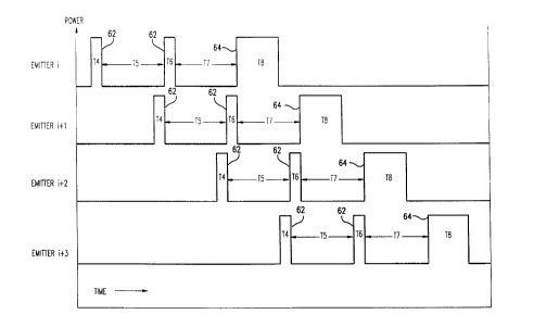
Figure 6 is a timing diagram illustrating how pulses are
interleaved in time according to a preferred embodiment of the present
invention. Figure 6 is similar to Figure 5, except that in Figure 6, two
precursor pulses are applied to each of the emitters (or emitter banks). For
any given emitter (or emitter bank), during the relaxation time between
the precursor pulses and the print pulse, the precursor pulses of
subsequent emitters (or emitter banks) are interleaved. Thus, a second
precursor pulse of a second emitter and a first precursor pulse of a third
emitter may be interleaved in time between a second precursor pulse and a
print pulse of a first emitter. In a preferred embodiment, a second
precursor pulse of a third emitter and a first precursor pulse of the fourth
emitter are interleaved in time between a print pulse of a first emitter and
a print pulse of a second emitter. Because the pulses are interleaved in
time, there is never more than one pulse applied to any of the emitters at a
given time.
Figure 7 is a systems diagram illustrating an embodiment of the
present invention having a thermal ink jet printhead 68, a power supply
source 66 and a system controller 67. The thermal ink jet printhead 68 is
activated by two pulses which are interleaved in time and supplied to
different emitter banks 96. One of the pulses is controlled by the
corresponding data which is to be recorded. In the embodiment shown in
Figure 7, there are 128 emitters, organized into 32 emitter banks 96 of four
emitters per bank, the electrothermal transducers 46 which cause the ink
emission are electrically attached to a power supply source 66 via the burn
-9- 2148994
voltage line 70. Each electrothermal transducer 46 is also attached to a
power transistor 51 which switches the burn voltage 70 to ground through
the transducer 46.
The emitters are grouped into emitter banks 96 in order to
achieve a good balance between the instantaneous power requirements,
the number of external electrical leads which must be attached to the
printhead, and the time required to provide power pulses to all of the
emitters. The bank organization creates a set of emitters which can be
pulsed individually without exceeding the capacity of the power supply
source 66 and power carrying lead 70. At the same time, the bank
organization allows the data to be presented to the printhead in units of
the number of emitters in a bank 96, four in the embodiment of Figure 7,
saving interconnection leads. Also since the several emitters of a bank 96
are able to be pulsed simultaneously, the time required to cycle through all
of the emitters of the printhead is reduced to the time needed to cycle
through the banks 96. In the embodiment of Figure 7 there are 32 banks
96 with four emitters each, 128 emitters in all. Thus, the banking
organization allows the 128 emitters to be pulsed by a power source sized
to supply only four emitters simultaneously, the data to be handled in units
of four bits, and the full set of emitters to be addressed in 32 time
subunits.
A predriver circuit 74 provides the necessary gate voltage level to
the power transistor 51 so that it will turn fully on. The predriver circuit
74
functions like a logical AND gate having logical inputs from a data line 94
and the emitter bank selection shift register 90. The burn voltage and the
gate voltage applied to power transistor 51 may be higher than a normal
logic level of 3 to 5 volts. Typically the burn voltage is 35 volts to 45
volts
and the gate voltage output of the predriver 74 is 7 volts to 14 volts. The
predriver circuit 74 also serves as the interface between the low voltage
logic circuitry and the higher voltage circuitry needed to apply power
pulses to the electrothermal transducers 46. The remainder of the circuitry
shown in Figure 7 is operated at a typical logic level of 3 to 5 volts.
The data management and power pulse scheduling functions
are accomplished by the other major circuit elements shown in Figure 7. A
system controller 67 accepts from an image source (not shown) on line 160,
a system user interface (not shown) on line 162, such as a user panel or soft
display interface, and one or more auxiliary control factor sources (not
shown) on line 164, for example a temperature sensing and control system
-1°- 21 X8994
or an input media monitoring system as well as other signals fro managing
the total operation of the liquid recording apparatus (not shown). The
overall system controller 67 provides the remaining circuitry with signals
conveying data on line 71, direction of printing, also on line 71, data bit
shift clocking on line 77, drop emission timing (ENABLE signals) on line 73,
and logic circuit reset on line 75. The system controller 67 also manages
the burn voltage power supply 66 on line 79. The data is entered via a
DATA/DIRECTION LINE 71 in four bit serial fashion where it is latched by O-
bit serial data latch 82. At the proper time, controlled by the load clock,
LCLK, the four bits of data are transferred and latched to the 4-bit parallel
data latch 80. The LCLK signal as well as the other timing signals PHASE A,
PHASE B, SCLK N, and SCLK P are generated by the timing generator circuit
86. The function of the timing generator circuit 86 is described in detail
below. The data is further controlled by a set of four logical AND gates 78,
which all have an additional logical input, the PHASE B signal. Therefore,
only if the PHASE B signal is high will the four bits of data be presented to
the inputs of four logical OR gates 76 and subsequently appear on the four
data lines 94.
In the embodiment of Figure 7 there is provided a signal PHASE
2° A as an output from timing generator circuit 86, which can also be
presented to all of the logical OR gates 76. This PHASE A signal is not
controlled by the data, but, if presented to the logical OR gates 76, will be
passed out to all of the data lines 94. Therefore, the predrivers 74 receive
logical inputs from the data lines 94 for either the case of PHASE B AND
DATA being high (logically true) or PHASE A being high (logically true). By
controlling the timing relationships of PHASE A and PHASE B, the
predrivers 74 can thus receive two power pulse commands, one which is
the same for every emitter of the emitter bank 96 and derives from PHASE
A, and a second which is controlled in time by PHASE B but is given only for
emitters which also have DATA logic highs.
The phase A power pulses are precursor pulses that change the
temperature of the ink near the heating element 46, thereby affecting the
amount of ink emitted when an emitter receives a subsequent phase B
AND DATA power pulse. The system controller 67 can modify the duration
of the phase A power pulses via the enable signal. This may be
accomplished by sensing the temperature of the ink near the emitter, or by
sensing the temperature of the printhead near the emitter, with a
-11- 21 ~8~~~
temperature sensing element, such as in U.S. Patent Application No.
08/220,720 to Stephany, which has previously been incorporated herein by
reference.
There are many potential applications of the phase A precursor
pulse. It can be used in conjunction with a temperature management
system to adjust for different printhead and environmental temperature
conditions so as to maintain constant ink emission. It can be used to
selectively increase or decrease quantity of ink emission in response to a
user's desire for darker or lighter images. It can be used to adjust for color
balance in a recorder with multiple color printheads. It can be used to
adjust ink emission for different ink formulations loaded into the
printhead or for different print media such as overhead projection
substrates or different paper types. These and many other possible uses of
precursor pulses are determined by the overall printer system controller 67.
Embodiments of the present invention enable such precursor pulses to be
applied to emitters with improved time efficiency, resulting in faster
recording speed than conventional devices.
Power pulsing of individual transducers 46 within an emitter
bank 96 is controlled via an input to the predrivers 74 which are connected
to the four data lines 94. A second input to the predrivers 74 is shared by
all of the predrivers 74 of an emitter bank 96. There is provided a separate
second predriver input line 92 for each of the 32 emitter banks 96 shown in
the embodiment of Figure 7. These second predriver input lines 92 are
controlled by the bank selection shift register 90. The bank selection shift
register 90 has 32 outputs, F1 - F32, one for each emitter bank 96. When
one of the output lines F1 - F32 is logically high, the corresponding emitter
bank 96 is able to be pulsed since the predrivers 74 of the corresponding
bank are now able to close the corresponding power transistor switches 51
in response to signals from the data lines 94. The bank selection shift
register 90 functions to allow only one emitter bank 96 to be pulsed during
any instant of time since the power source has been sized to accommodate
only one emitter bank 96 at a time, to synchronize the selection of an
emitter bank 96 with the proper set of 4 bits of data appearing on the data
lines 94 for that bank 96, and to cycle through all of the emitter banks 96
so that there is an opportunity for every emitter to be activated by both
PHASE B pulses and PHASE A pulses. The bank selection shift register 90
further provides for the interleaving of the pulses between the emitter
-12-
2168994
banks 96, as illustrated in Figure 5, so that full cycling through all of the
banks 96 for the two pulses can be accomplished much more rapidly than if
the pulses were not interleaved, as in the prior art illustrated in Figure 3.
The bank selection shift register 90 is also bidirectional so that the
selection
of emitter banks 96 can proceed from the first bank to the last bank or vice
versa. This is useful for printing as illustrated in Figure 1, whereby the
printhead 4 is allowed to print when traversing in both right to left and
left to right directions of the carriage 20. Further details about the design
of the bank selection shift register 90 are given below in the discussion of
Figures 9, 10 and 11.
The timing generator circuit 86 provides the signals: LCLK,
PHASE A, PHASE B, SCLK N, and SCLK P. The LCLK causes the 4-bit parallel
shift register 80 to latch whatever data is held by the 4-bit serial shift
register 82. The PHASE A signal allows all of the emitters of an emitter
bank 96 to receive power if the bank's bank selection line (F1 - F32) is
currently held high by the bank selection shift register 90. The PHASE B
signal allows each of the emitters of a bank of emitters 96 to receive power
if the data line 94 for the emitter is high and the bank's bank selection line
(F1 - F32) is being held high by the bank selection shift register 90. Shift
clock signals SCLK N and SCLK P are non-overlapping logical inverses of
each other and cause the bank selection shift register to advance a token
bit thereby shifting the selected bank of emitters 96 along the 32-bank
row. The bank selection shift register 90 operates bidirectionally so that
the banks of emitters 96 can be selected in opposite order for printing in
bidirectional carriage printer fashion, as illustrated in Figure 1.
The timing generator circuit 86 derives its output signals from
the logic input on the ENABLE LINE 73 and the non-overlapping logical
inverse of the signal input on ENABLE LINE 73, both are provided by the
non-overlapping signal generator 84, and from the signal input on the
FUNCTION CLEAR LINE 75, which serves to logically reinitialize the timing
generator circuit 86 at the beginning of each printing cycle. Both the
ENABLE and the FUNCTION CLEAR signals are provided by an overall
printer system controller 67. The timing generator 86 is a signal passing
circuit which constructs the output signals from specific logic level
transitions present in the ENABLE input signal. The function of the timing
generator circuit can be further understood by reference to Figure 8, a
timing diagram of the signals which have been described above.
-13- 2 ~ 68994
Figure 8 shows the timing relationships among the following
signals: FUNCTION CLEAR (FCLR), ENABLE, PHASE A, PHASE B, F1, F2, F3, F4,
SHIFT CLOCK (SCLK N and SCLK P), and LOAD CLOCK (LCLK). Figure 8
illustrates the timing relationships for the case of sequentially selecting
emitter banks 96 from BANK 1 to BANK 32. Bank selection signals are
shown for BANKS 1 - 4 only. Signals for BANKS 5 - 32 would be generated
in a continuing sequence in like manner to the signals F1 - F4 before a new
FCLR logic transition was sent by the printer system controller. The falling
logic level edge 120 of the FCLR signal initializes the circuitry shown in
Figure 7. It causes all of the other signals shown in Figure 8 to be in the
low
state except F1 and SCLK N, which are initialized high for this case of
sequencing emitter banks 96 in the order BANK 1 to BANK 32. For the
opposite direction of sequencing, F32 and SCLK N are initialized as high
when the falling FCLR edge 120 occurs.
The ENABLE signal has a repeating sequence of four logic
transition edges: 122, 124, 126, and 128. ENABLE logic rising edge 122 is
passed by the timing generator circuit 86 to its PHASE A output causing the
Phase A rising logic edge 130 and to its LCLK output causing the LCLK rising
logic edge 132. The rising edge 132 of LCLK latches whatever DATA is
appearing at the output of serial data latch 82 into parallel data latch 80.
In Figure 8 the first instance of the rising edge of PHASE A 130 results in
power being applied to all of the jet transducers 46 of jet BANK 1 since F1 is
also logically high.
The first logic falling edge 124 of the ENABLE signal is passed by
the timing generator 86 to its PHASE A output. The PHASE A signal is
thereby sent low as indicated by the PHASE A falling edge 134. This ends
the PHASE A power pulse to the selected emitter bank 96, BANK 1 for the
case illustrated by Figure 8. The logical inverse of this first logic falling
edge 124 of ENABLE is also available from the non-overlapping signal
generator 84 and is passed by the timing generator circuit 86 to its SCLK P
output where it causes the SCLK P rising logic edge 136. The SCLK P rising
logic edge 136 is important to the interleaving function of the Figure 7
circuitry of this preferred embodiment of the invention. The first logic
falling edge 124 of ENABLE, translated into the rising edge 136 of SCLK P
by the timing generator 86, is used to insure that power pulses related to
the PHASE A signal and applied to one of the emitter banks 96 are
terminated before power pulses related to the PHASE B signal are applied
14
to the next emitter bank 96. The logical inverse shift clock, SCLK N, is also
provided by the timing generator 86 and is also used internally in the bank
selection shift register 90 to advance a logical high bit along the cells of
the
shift register. The bank selection signals F1 - F4 will be further explained
below in conjunction with the more detailed explanation of the bank
selection shift register 90 using the additional Figures 9 - 11.
The second logic rising edge 126 of the ENABLE signal is passed
by the timing generator circuit 86 to its PHASE B output, causing the rising
logic edge 138 in the PHASE B signal. As described above, the PHASE B
signal is logically ANDED with the DATA present in the parallel data latch
80 and therefore determines when DATA will be presented to the OR gates
76 for presentation to the data lines 94.
The second logic falling edge 128 of the ENABLE signal is passed
by the timing generator 86 to its PHASE B output, shutting off the
presentation of DATA to the OR gates 76, to its SCLK P output and to its
LCLK output. In the case of the LCLK output, the logic falling edge 140
allows new DATA to be presented to the parallel data latch 80. The use via
the SCLK P output of the second logic falling edge 128 of the ENABLE
signal in the bank selection shift register 90 will be explained in more
detail below in conjunction with the explanation of Figures 9 - 11.
The ENABLE signal continues to repeat the same sequence of
rising and failing logic transitions 122 - 128 causing the events of data
latching, PHASE A power pulse firing, PHASE B AND DATA power pulse
firing, and sequencing through the banks of emitters 96 until all 32 banks
of emitters have been selected for one PHASE A and one PHASE B time
period. The bank selection shift register 90 described below further
functions to interleave the two pulses to a bank of emitters with the pulses
to the adjacent banks of emitters, thereby allowing the pulsing of all of the
128 emitters to proceed in a rapid, time efficient fashion.
Three other circuits are illustrated in Figure 7 which are used in
this preferred embodiment of the invention. The non-overlapping signal
generator 85 controls the operation of the 4-bit serial data latch 82. A BIT
SHIFT signal via line 77 is provided by the overall printer system which is
passed by the non-overlapping signal generator 85 to the 4-bit serial data
latch 82 in non-overlapping original and logically inverted forms. The
overall printer system can then present DATA to the DATA/DIRECTION line
71 and clock this DATA into the 4-bit serial data latch 82 at a clock rate
15
determined by the BIT SHIFT line 77. This can be done any time when the
LCLK signal output of the timing generator circuit 86 is high without
affecting the rest of the data path circuitry elements 80, 78 and 76.
In Figure 7, a direction signal generator 88 is shown which
provides to the bank selection shift register 90 the signals DIR N and DIR P.
The direction signal generator 88 derives from the DATA/DIRECTION line
71 and FUNCTION CLEAR line 75 signals provided by the overall printer
system controller 67. This signal establishes whether the bank selection
shift register 90 will advance from emitter BANK 1 to emitter BANK 32 (DIR
N, high; DIR P, low) or in the opposite direction from emitter BANK 32 to
emitter BANK 1 (DIR N, low; DIR P, high). The DIR N/P state is set by the
logical state of the DATA/DIRECTION line 71 at the time the FCLR makes its
rising logic transition 121 shown on the timing diagram of Figure 8. Until
the next FCLR signal is sent by the printer system controller 67, the
DATA/DIRECTION line 71 is used to shift in DATA as described above and
the direction signal generator ignores the data signals on this shared line.
The printer system controller 67 provides the proper direction signal at
each FCLR rising logic transition 121.
In Figure 7 a non-overlapping signal generator 87 accepts the
FUNCTION CLEAR signal from the printer system controller 67 and
generates non-overlapping logical inverses of FUNCTION CLEAR (FCLR and
FCLR BUS). FCLR BUS, the inverse of FCLR, is used internally by the bank
selection shift register 90 to initialize internal states of the cells of the
shift
register 90. This will be explained further below.
Further details of the bank selection shift register 90 are shown
in Figures 9 - 11. Such registers are well known in the art. In the simplest
form they consist of internal logic cells which can pass and hold a logic
state from one cell to the next. Shift registers which are used to transfer
logic control along a succession of outputs are also well known as token bit
shift registers. The cells of the shift register are all set to logic level 0
(low)
and then a single logical value of 1 (high), called the token, is shifted from
cell to cell causing the outputs of the cells of the shift register to output
the
logical 1 (high) moving with each shifting clock event from output to
output along the shift register. The bank selection shift register 90 is a
simple token bit shift register with two additional functions. First, it can
operate bidirectionally so it has circuitry in each cell which can pass the
token bit either to the cell numerically above or numerically below itself.
-16- 21 b899~
And second, to perform the interleaving function of the invention, the
bank selection shift register 90 also passes the token bit forward one cell
for part of the ENABLE signal as generated by the timing generator 86
outputs SCLK N and SCLK P.
Figure 9 shows the internal organization of the bank selection
shift register 90 of Figure 7 in more detail. There are 32 identical emitter
bank cells 100 of the bank shift selection register 90, one for each of the
emitter banks 96, and two end cells 98 to properly initialize the action of
the bank selection shift register 90 in whichever direction it is being
operated. Each of the bank cells 100 has four inputs and four outputs
which link adjacent cells to one another and are internal to the bank
selection shift register 90. Each of the bank cells 100 also has five signal
inputs which come from the printer system controller 67 via the FCLR
generator 87 (FCLR BUS), via the direction signal generator 88 in Figure 7
(DIR N, DIR P) and via the timing generator 86 in Figure 7 (SCLK N, SCLK P).
Finally, the bank cells 100 each have an output line FN (F1 - F32), which is
directly connected to the predrivers 74 of the corresponding emitter banks
96. As described earlier, when a logic high level appears on one of the
bank cell output lines F1 - F32, the predrivers 74 of the corresponding
emitter bank 96 then close the power transistor switches 51 of that emitter
bank 96 if either PHASE A or DATA AND PHASE B high signals are
presented by OR gates 76 to the data lines 94.
The four internal input and four output lines shown for each of
the cells 100 of Figure 9 arise because, firstly, for simplicity of design and
understanding when constructing shift registers of many cells, it is helpful
to designate lines which pass signals from one cell to the next as having
both an output end and an input end even though once actually assembled
they will be the same wire or conductor run inside the circuit. Secondly,
since the bank selection shift register 90 is bidirectional, there are two
sets
of inputs and outputs, one for the "forward" direction (DIR N, high; DIR P,
low) and one for the "reverse" direction (DIR N, low; DIR P, high). Finally,
because of the need to interleave the power pulses going to one emitter
bank 96 with those going to an adjacent emitter bank 96, both a main
control token signal and an advanced or prepulsing token signal are
needed. Thus the eight internal input and output signal lines shown in
Figure 9 for each bank cell 100 are labeled in the following fashion. The
suffix IN or OUT indicates whether the signal is being used as an input (IN)
- ~16899v
to the particular bank cell 100 or passed out (OUT) of the particular bank
cell 100. The three letter root (FWD) or (REV) designates whether that line
is active for the forward (FWD) direction of shift register operation (DIR N,
high; DIR P, low) or for the reverse (REV) direction of shift register
operation (DIR N, low; DIR P, high). Finally the outputs and inputs with the
additional prefix (PP) are the lines which carry the advanced token
(prepulse token) ahead of the main token lines (without prefix). It is these
PP signal lines (PPFWDIN, PPFWDOUT, PPREVIN, PPREVOUT) which will
allow a bank of emitters 96 to receive power during the PHASE A signal,
earlier in time then that emitter bank 96 receives its power based on the
PHASE B AND DATA signal. The main token signal lines (FWDIN, FWDOUT,
REVIN, REVOUT) control the bank selection for receiving power during the
PHASE B AND DATA signal period which results in emitters actually
emitting print drops of ink. The power received by an emitter bank 96
during the PHASE A period is generally intended to precondition the ink
temperature thereby affecting the volume and velocity of the ink which
will be emitted for emitters subsequently receiving power during the
bank's PHASE B period.
The two end cells 98 shown in Figure 9 supply the initial tokens
for both the main token and the prepulse token inputs to either the BANK
1 cell 100 or to BANK 32 cell 100 depending on the direction of operation
being determined by the DIR N and DIR P signal lines. For the example
shown in the timing diagram of Figure 8, the DIR N/P lines are set to
operate the bank selection shift register 90 from BANK 1 to BANK 32. In
this case end register 98 connected to the BANK 1 cell 100 is active. In
response to the rising logic high edge of the FCLR BUS (the inverse of the
failing logic edge 120 shown for the FCLR signal in Figure 8) the end
register 98 will provide a pretoken signal on its PPFWDOUT line to the
PPFWDIN line of the BANK 1 shift register cell 100. This PPFWDOUT signal
is passed by the BANK 1 cell 100 to its output F1 as a logic high, shown in
the timing diagram Figure 8 as high level 142 on the F1 line. The end cell
98 will also provide on its signal line FWDOUT the first main token to the
BANK 1 cell 100 on its input line FWDIN. The end cell 98 derives this initial
main token from the FCLR BUS signal. The initial token is latched by the
rising logic edge of SCLK P which in turn has been generated by the timing
generator circuit 86 from the first falling logic low edge 124 of the ENABLE
signal.
_ 18_
~~ X8994
Further detail on the circuit design and operation of the bank
cell 1 00 and the end cell 98 can be understood from Figures 10 and 11. In
Figure 10, the circuit diagram of a bank cell 100 illustrates the eight
internal signal lines, the five external signal inputs and the one external
output, FN (F1 - F32) together with the pass transistors 102, inverters 104,
and logic function circuits 106 - 112 needed create the signals described
above. For simplicity of understanding, the direction of operation of the
shift register can be ignored by considering the operation for one direction
since the operation in the opposite direction is the same except that the
physical location of the input and output lines changes. Only one set of
lines, either FWD lines or REV lines is physically active at any time. For the
timing diagram example illustrated in Figure 8, the forward direction has
been selected and so the FWD lines of the cell 100 in Figure 10 are being
used. The two signal pass transistors 102 controlled by DIR N are therefore
on, allowing signal to pass into the cell from the FWDIN and PPFWDIN
lines. The two signal pass transistors 102 controlled by DIR P are off,
stopping signals from passing into the cell from the KEVIN and PPREVIN
lines.
At the lower portion of the bank cell 100 circuit it can be seen
that a signal appearing on the PPFWDIN line is passed by transistor 102 to
NAND gate 112 whose output is the bank selection signal, FN. FN is
connected to the corresponding set of predrivers 74 for the corresponding
emitter bank 96. Therefore the preceding cell can affect the FN signal of a
current cell by holding a low signal on PPFWDIN, that is on its own
ppFWDOUT line.
The SCLK N and SCLK P lines each control two signal pass
transistors 102. The two signal pass transistors 102 controlled by SCLK N
control the entry of signals from FWDIN into the cell 100 at circuit point S1
in Figure 10. The main token is sampled and latched when SCLK N has
rising logic edges such as SCLK N edge 144 in Figure 8. The two signal pass
transistors 102 controlled by SCLK P control the presentation of output
signals to FWDOUT in Figure 10. Signals appearing at FWDOUT are
presented to the next shift register cell 100 via its FWDIN line. FWDOUT
signals are also presented to the FN line via NAND gate 110 and NAND gate
112.
19 ~ ( 68994
Therefore high signals at FWDOUT both allow power pulsing of the
corresponding bank of emitters 96 and provide a high token signal for the
next cell on the next cell's FWDIN line.
In addition when the FWDIN line is sampled at circuit point S1
(by SCLK N rising and SCLK P falling) and if it is a logic level 1, the main
token is present. Then, PPFWDOUT is asserted low by NAND gate 108 until
the SCLK's change state again. This is the prepulse token passing event
described above. It occurs when a cell has received a logical high signal,
the main bank selection token, via its FWDIN line which is latched at circuit
point S1. When SCLK N falls low again, and SCLK P goes high, the main
token signal high is presented to both FWDOUT for latching by the next
cell and to FN to allow pulsing of the corresponding bank of emitters 96
during PHASE B as described above.
Thus the action of the cell 100 when operating in the forward
direction is to accept a high signal on its FWDIN line if one is present from
the previous cell's FWDOUT line during one logical high period of SCLK N
and then to provide a high signal to the cell's FN line and FWDOUT line
during the next logical low period of SCLK N. During the high period of
SCLK N (and so the low period of SCLK P), the cell passes a logic low level to
the next cell's PPFWDIN line resulting in an F(N + 1) high at the output of
that next cells NAND gate 112.
The cell output line FWDOUT is held logically low by NOR gate
106 which has the FCLR BUS signal line as one of its inputs. Only the
passage of the main token high signal through latch point S1 overrides this
low being set by FCLR BUS and NOR gate 106.
Finally, the above explanation of the operation of the main cell
100 of the bank selection shift register 90 applies equally to the case of the
reverse direction of the operation (DIR N, low; DIR P, high) except that the
REV signal lines are substituted for the corresponding FWD signal lines.
The circuitry controlled by SCLK N, SCLK P and FCLR BUS operates in the
identical fashion in the reverse direction.
The above explanation of the main cell 100 operation is largely
applicable to the end cell 98 diagrammed in Figure 11. An end cell 98 is
necessary to begin the process described above of main token acceptance,
passing the token forward to allow prepulsing, and passing the main
token. The end cell 98 shown in Figure 11 is similar to the main cell 100 in
that its circuit signal point S2 is equivalent in design and behavior to the
-2°- ~ 16894
circuit points S1 discussed above in conjunction with the main bank cell 100
circuit. The end cell 98 has an additional earlier stage which features NOR
gate 114 with inputs from FCLR BUS and from ground (GND, logic low or 0)
controlled by a SCLK P signal pass transistor 102. This first stage of the
circuit generates and latches at circuit point S3 a logic low during the FCLR
BUS high signal. This logic tow at S3 persists during the initial SCLK P low
time period (see the timing diagram in Figure 8) and is passed forward on
the PPFWDOUT line to the BANK 1 cell 100. This allows the first bank of
emitters 96 to receive power pulses during the first instance of the PHASE
A signal. A logic high state is also latched at circuit point S2 by the FCLR
BUS signal. Upon the next transition of the SCLK N and P lines (SCLK P
going high, SCLK N going low) this logic high is passed to the FWDOUT line
of the end cell 100, providing the initial token to the FWDIN line of the
BANK 1 cell 100. The BANK 1 cell 100 is not ready to pass this signal to its
F1
NAND gate 112 so no power pulsing occurs for this very first PHASE B
period. The sequencing of bank selection for PHASE A and PHASE B power
pulses then continues in the fashion described above in the explanation of
the bank selection main cell 100. The timing diagram in Figure 8 shows the
interleaved FN signals generated by the bank selection shift register 90 for
the first 4 emitter banks 96.
The above explanation of a preferred embodiment of the
invention for the case of emitter bank activation by two power pulses can
be extended to the case of three or more pulses. In the extended case the
ENABLE signal would contain logic transition edges sufficient to define a
PHASE period for each pulse and the bank selection shift register 90 would
be expanded to pass forward a token for each pulse.
A second preferred embodiment of the invention is shown in the
system diagram of Figure 12. The circuit is similar to the embodiment
diagrammed in Figure 7. All like elements of this second embodiment are
numbered in like manner to the elements of Figure 7. There are three
differences in this second embodiment all related to enabling the data to
control which emitters are pulsed within an emitter bank 96 during PHASE
A, in like manner to the previous embodiment, wherein the data
controlled the individual emitter pulsing during PHASE B. This new
function of allowing PHASE A power pulses only for emitters with
corresponding data values of logical 1 (true) is accomplished by expanding
the input serial data latch to the 8-bit latch 83, adding a second 4-bit
-21 -
~16g99~
parallel data latch 80 and adding four additional AND gates 78. The AND
gates 78 perform the logical operation of ANDING the data presented by
the lower 4-bit parallel data latch 80 with the PHASE A signal from the
timing generator circuit 86. The outputs of the four lower AND gates are
connected to the OR gates 76. In operation 4 bits of DATA are shifted into
the lower four cells of 8-bit serial register 83. These bits are loaded into
the
lower 4-bit parallel data latch 80. They are ANDED with the PHASE A signal
so that only signals which are logically DATA AND PHASE A will be
presented to the OR gates 76 for presentation to the data lines 94. A next
set of 4 bits of DATA is then shifted into 8-bit serial register 83, moving
the
previous 4 bits of DATA into the upper half of latch 83. These bits are now
latched into the upper 4-bit parallel data latch 80. They are now ANDED
with the PHASE B signal in the upper four AND gates 78 so that only signals
which are logically DATA AND PHASE B are presented to the OR gates 76
for presentation to the data lines 94. In this fashion the DATA for each
emitter is preserved during both PHASE A and PHASE B power pulse
periods and only emitters which are to be printed receive power from
either pulse. This embodiment of the invention therefore has the
additional advantage of saving power as well as saving recording time
through the interleaving circuitry.
The pulse interleaving circuitry operates exactly the same for this
second embodiment as described above for the embodiment diagrammed
in Figure 7. The embodiment of Figure 12 can also be extended to the case
of three or more activation pulses by adding a set of serial and parallel
data latches and AND gates for each activation pulse PHASE.
A third embodiment of the invention can be envisioned in which
the ENABLE signal logical transition edges are changed by the printer
system controller 67 and/or the power applied via the BURN VOLTAGE
lines in Figures 7 and 12 is changed by the overall printer system controller
67 and the power supply source 66 to further modulate the power being
applied to the liquid emitters. In such embodiments, the function of
interleaving the pulses in time and controlling some or all of the pulses by
the data can be carried out in like fashion to the embodiments described
above.
Further, while the preferred embodiment of the invention
described above interleave pulses applied to banks of emitters, the
22
preferred embodiments could be easily modified to interleave pulses
applied to each emitter.
While this invention has been described in conjunction with
specific embodiments thereof, it is evident that many alternatives,
modifications and variations will be apparent to those skilled in the art.
Accordingly, the Preferred embodiments of this invention, as set
forth herein, are intended to be illustrative, not limiting. Various changes
may be made without departing from the spirit and scope of the invention
as defined in the following claims.