Note: Descriptions are shown in the official language in which they were submitted.
2 i 69308
SUBSTRATE BASED ARRAY CONNECTOR
BACKGROUND OF THE INVENTION
1. Field of the Invention
This invention relates to optical communication fiber connectors, and in
particular to connectors for a plurality of optical fibers which are
stabilized by a
substrate.
2. Description of Related Art
The efficient movement and management of information now requires local
area networks within buildings and wide area networks across the nation which
provide on-line access to data bases and communications services. The concept
of
an information highway is developing into hardware which will provide wide
bandwidth services to every home. Optical fibers provide great bandwidth which
is
capable of distributing multimedia services in a noise-free and secure
network. The
distribution of these services will take place in the loop plant of local
telephone
companies, or others in competition with them, to connect nearly every home
and
office to the information highway.
A variety of optical fiber designs already exist together with connectors for
them. The fibers may be designed for single-mode or multi-mode transmission
with
cladding or outer diameters of 125 microns and core diameters of approximately
2 0 five microns or 65 microns, respectively (one micron equals one millionth
meter).
Other core and cladding diameters are feasible.
There are coupling losses when an optical fiber needs to be connected to
another optical fiber or to an opotelectronic apparatus. A permanent
connection
whereby the glass fibers are butt-fused together with a flame is impractical
for most
2 5 applications. For non-permanent connections, losses in the connection
arise from
misalignment of the two axes by being off axis with one another, by having
their
axes at an angle to one another, by having their ends separated by too great a
distance, or any combination of these three. Another possibility for loss is
the
mismatch between the refractive index of the fibers and an intervening air gap
3 0 which is left between the ends of the fibers. This loss is often minimized
by an
~ 169308
- 2 -
index-matching gel or silicone fluid which fills the gap.
The requirements placed upon the connector are, therefore, to locate the axes
within plus or minus 0.5 microns or plus or minus two microns of each other,
depending upon the mode, and to maintain angular orientation of the two axes
to
within a few degrees. These tolerances are required to keep the loss per
connection
to less than a few tenths of a decibel. These tolerances become tighter as the
number of connectors in series increases.
Micron type tolerances are common in semiconductor processing, and there
is an embedded base of fiber optic connectors which take advantage of
semiconductor fabrication tolerances and the ability to etch grooves into
silicon to
form V-groove connectors which keep an array of optical fibers accurately
spaced
apart. In addition to accurate spacing, the silicon member provides
dimensional
stability because it has a low coefficient of thermal expansion and because it
is
insensitive to moisture. Both of these properties are important in the
environment
of the loop plant where temperatures can range from -40 degrees Fahrenheit to
160
degrees in a cable vault, and where the connector could be under water. So
there is
a well working etched silicon connector technology, but it is very expensive
when
considering all the connectors in series from a source to the final piece of
app aratus.
2 0 Naturally, attempts have been made to reduce this cost by using the
precision of an etched silicon master to electroform a molding die for plastic
connectors. Their construction consists of a pair of ferrules with a gum boot,
two
guide pins that align the ferrules to each other, and a clamp spring which
holds the
assembly together. Reliance upon the guide pins penetrating two plastic bodies
for
2 5 precise location lowers the coupling efficiency, and therefore the yield,
for single
mode fiber connections. The thermal expansion of the plastic body, typically
16
parts per million per degree Centigrade, does not match the embedded base of
etched silicon connectors whose expansion is 2.3 ppm/deg. C. These connectors
do
lower cost, typically by 50%, but they are susceptible to dimensional changes
as
3 0 both temperature and humidity cycle in the conditions which are typical in
the loop
X169308
- 3 -
plant. The release of residual molding stresses may also cause warp in the
plastic
over time.
Accordingly, there is an increased need for a moderate cost optical fiber
connector which precisely locates the axes of the fibers and which maintains
that
alignment in hostile environmental conditions. Additionally, the connector
should
more closely match the thermal expansion of the embedded base of etched
silicon
connectors.
3. Summary of the Invention
The present invention relates to connectors which restrain optical fibers in a
manner which provides precise alignment, hence less coupling loss, and which
maintains this alignment over time and with large variations in temperature
and
humidity. The required dimensional stability is achieved by using a rigid
substrate
whose relative thickness, modulus of elasticity, and coefficient of thermal
expansion
are selected to dominate the mechanical characteristics of the connector.
The optical fibers are restrained by features which are formed into or are
defined by a thin layer of an encapsulant which is supported by the rigid
substrate.
The precision of these features is controlled by a molding die which repeats
these
features over a large number of connectors to reduce cost. These features may
be
in the form of a V-groove formed into the encapsulant by the molding die so
that
2 0 two optical fibers lie in the same V-groove with their ends facing one
another.
In one embodiment of the invention, a feature such as a V-groove, or a
series of them, is defined by an encapsulant which is supported by the upper
surface of the substrate.
In another embodiment of the invention, the encapsulant surrounds the
2 5 substrate and defines a feature on its outer surface which is adapted to
restrain an
optical fiber.
In a further embodiment of the invention, a rigid cover overlaps and
restrains optical fibers which are held by V-grooves in an encapsulant
covering a
substrate.
30 In.yet another embodiment of the invention, a metal lead frame is attached
CA 02169308 2001-10-02
- 4 -
to a substrate to aid in the mass production molding of a surrounding
encapsulant
which defines features on its outer surface with the precision of a molding
die.
In still another embodiment of the invention, the lf;ad frame and substrate
are
made from the same material and are integral with each oi;her. The encapsulant
is then
molded around the combination in the operation which defines the features.
In another embodiment of the invention, two substrate-encapsulant connectors
are inverted to one another so that their features align to form a nearly
closed cavity
which restrains an optical fiber. Securing means may hold. the connectors
together.
In accordance with one aspect of the present invention there is provided a
connector for an optical fiber comprising: a rigid rectangular substrate
having a
substantially planar upper surface; an encapsulant surrounding the substrate;
a feature,
disposed within the encapsulant above the upper surface o~f the substrate, for
receiving
at least part of the optical fiber therein and retaining the optical fiber in
a fixed
orientation with respect to the substrate; and a rigid cover., disposed above
the feature,
that contacts the optical fiber and restrains the optical fiber in the
feature, wherein the
feature is a groove.
In accordance with another aspect of the present invention there is provided
an
optical fiber cable connector assembly comprising two connectors wherein each
connector comprises: a rigid rectangular substrate having a substantially
planar upper
2 0 surface and a substantially planar lower surface; a lead frame attached to
the lower
surface of the substrate; an encapsulant surrounding the substrate and a
portion of the
lead frame nearest to the substrate; and a feature, disposedl within the
encapsulant
above the upper surface of the substrate, for receiving at 1<~ast part of the
optical fibers
therein; wherein one connector is inverted and positioned adjacent the other
thereby
2 5 aligning each feature and forming a cavity which is adapted to restrain
the optical
fibers.
These and other features and advantages of the invention will be better
understood with consideration of the following detailed description of the
preferred
embodiments taken in conjunction with the accompanying; drawings.
3 0 4. Brief Description of the Drawings
FIGS. 1A, and 1B are sectional views of two embodiments of the invention;
CA 02169308 2001-10-02
- - 4a -
FIG. 1 C is a perspective view of optical fibers being restrained by a groove
in a
connector;
FIG. 2 is a sectional view of apparatus in accordance with another embodiment
of the invention;
FIGS. 3A and 3B are sectional views of other embodiments of the invention;
and
FIGS. 4A, 4B, and 4C are sectional views of connector assemblies in
accordance with other embodiments of the invention.
The drawings are not to scale.
5. Detailed Description of the Preferred Embodiments
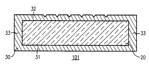
Referring now to FIG. 1A, there is shown apparatus 100 in accordance with
one embodiment of the invention. Substrate 20 has an upper surface 22, and a
lower
surface 21. The upper surface 22 of the substrate supports encapsulant 30
which has
an outer surface 39 which is generally planar except for one or more features
40 which
are adapted to restrain an optical fiber. The features may protrude from the
planar
surface, but in this embodiment of the invention they are
~1b93Q8
- 5 -
formed into the thickness of the encapsulant to define a V-groove with a first
side
41 and a second side 42 which meet at apex 46 to define an included angle
which
may be from 45 to 120 degrees. Sides 41 and 42 are generally planar, extend
upward to intersect the outer surface at intersections 43 and 44,
respectively, and
are sized to accommodate the ends of round cylindrical optical fibers so that
the
ends of the fibers face each other in close proximity. Referring now to FIG.
1B,
there is shown apparatus 101
in accordance with another embodiment of the same invention wherein
encapsulant
30 completely surrounds substrate 20 so that lower web 31 and upper web 32 of
the
encapsulant have approximately the same thickness. End sections 33 cover the
sides of the substrate. The same reference numbers apply to elements which are
common to the various embodiments of this invention. Referring now to FIG. 1
C,
there is shown apparatus 102
which is a perspective view of optical fibers 15 and 16 being restrained by
one of
the features 40, a V-groove in this case, which are formed into the outer
surface 39
of the encapsulant. Referring now to FIG. 2, there is shown apparatus 200
which is a side view of another embodiment of the invention wherein optical
fibers
15 are shown restrained by sides 41 and 42 of a V-groove which is formed into
the
thickness of encapsulant 30. Rigid cover 50 further restrains the conductors
from
2 0 leaving the V-groove. This cover does not exert any lateral force that
could shift
the positions of the optical fibers in the V-grooves. Preferably, the thermal
expansion of cover 50 approximates or matches that of substrate 20. Typical
materials with low thermal expansion characteristics include silicon,
ceramics, and
glasses. Referring now to FIG. 3A, there is shown apparatus 300
2 5 which is a side view of another embodiment of the invention wherein a
metal lead
frame 70, being comprised of an outer planar section 71, an offset section 72,
and a
tab section 73, is bonded to the lower surface of the substrate. The purpose
of the
offset section is to locate the center of substrate 20 on the same plane as
the neutral
axis (not shown) of the composite while the outer sections of the lead frame
70 are
30 clamped at the parting line of the molding tool (not shown). Encapsulant 30
21b93~8
- 6 -
surrounds both the substrate, the tab section, the offset section, and a part
of the
outer section of the lead frame. Referring now to FIG. 3B, there is shown
apparatus 301 in accordance with another embodiment of the invention wherein
metal lead frame 370 is comprised of an outer section 371 which is similar to
outer
section 71 of apparatus 300. A substrate section 372 is connected to outer
section
371 but is thicker than the outer section or encapsulant 30, so that section
372
dominates the dimensional behavior of apparatus 301. Referring now to FIG. 4A,
there is shown apparatus 400
in accordance with another embodiment of the invention wherein two of the
connectors described as apparatus 300 above are disposed to restrain one or
more
optical fibers 15. Means for securing apparatus 400 together is shown as
element
420 in FIG. 4B, which together with two apparatus 300 constitute apparatus
401.
This means may be a clamp, a fastener, a latch, a sleeve, or any of the
securing
devices which are well known in the art. Apparatus 300 may not be identical to
each other, as shown, but could differ in that one contains a pin and the
other a
receptacle which could also secure them together. The operation of the
embodiments described above is predicated upon the rigidity and stability of
the
substrate with excursions of time, temperature, and humidity; and the ease of
precisely forming the features, such as V-grooves, in the encapsulant so that
even
2 0 single-mode i=ibers are held to a tolerance of plus or minus 0.5 micron in
the
conditions of the loop plant.
In a preferred embodiment the substrate is made of silicon whose coefficient
of
thermal expansion is 2.3 ppm/deg. C, which matches that of many connectors
already in use. The requirements of the substrate material are that it be
rigid, have
2 5 a low coefficient of thermal expansion, be dimensionally stable in humid
environments, be chemically inert over long periods of time, and not release
any
residual stress which could cause dimensional change or warp. These
requirements
argue strongly for an inorganic material such as silicon, a ceramic, or a
glass.
Silicon has all these properties and matches an embedded base of connectors in
use.
3 0 It need not be single crystal silicon, because its expansion is controlled
more by its
~ 1 ~93t~8
lattice type than by its crystallographic orientation, and it need not be
doped or
polished as in semiconductor fabrication. Indeed, scrap silicon from the
semiconductor industry could be used here to further lower the cost of
fabricating
this invention. Other possible materials include ceramics such as alumina
which
has a thermal expansion of 6.4 ppm/deg. C, or glasses which have low thermal
expansion such as those known under the trade names of Pyrex (3.2 ppm/deg. C),
Vicor (0.8 ppm/deg. C) or fused silica (0.6 ppm/deg. C). The alloy
commercially
known as "Kovar" has a thermal expansion coefficient (5 ppm/deg. C) which
matches ceramics and could also be used as a substrate material and for the
lead
frame-substrate combination shown in FIG. 3B. The alloy known as "Invar" has a
thermal expansion coefficient of 1.5 ppm/deg. C and it could also be a useful
substrate material.
The dimensions of the substrate are selected so that the mechanical properties
of the
connector are dominated by the substrate. Preferably the substrate is 20 mils
thick
and the encapsulant thickness is below 10 mils over the broad planar surfaces
that
cover the upper and lower surfaces of the substrate. The encapsulant may be
any
organic material, a preferred embodiment being an epoxy molding compound whose
viscosity is below 200 poise at its flow temperature. A biphenyl epoxy flows
at
170 degrees C and is well adapted to molding operations for thin small
orientation
2 0 packaging which is common in the semiconductor industry. The thickness and
modulus of elasticity of the substrate dominate the mechanical behavior and
stability of the apparatus when compared to the properties and thickness of
the
encapsulant. This advantage satisfies the needs of precisely maintaining the
location of the axes of optical fibers in hostile environments while also
matching
2 5 the thermal expansion properties of connectors already used in the
industry.
Thermal shock and temperature cycling tests have established the reliability
of this
configuration for external use.
The lead frame which is attached to the substrate is typically 6 mil thick
copper
alloy and is a device which is borrowed from semiconductor packaging to mass
3 0 produce these connectors with lead frame strips of multiple substrate
sites to reduce
z~~g~os
_8_
cost. The bonding to the substrate may be by adhesive, soldering, or thermo-
compression bonding which is common in electronic packaging operations. The
bonding may be eliminated if the function of the lead frame and substrate were
performed by a metal, typically a low expansion alloy, such as "Kovar", where
elements 371 and 372 of apparatus 301 are stamped in one operation. Spools of
substrates held together by the lead frame are then fed into the molding
operation
where the features, such as V-grooves are formed into the outer surface of the
encapsulant. The precision in locating the features is built into the molding
die,
which may be electroformed from a master of silicon which has been
photolithographically etched to micron tolerances which are commonly achieved
in
semiconductor processing. This cost is amortized over many molded connectors,
so
there is a cost advantage in practicing this invention over the connectors
which are
machined or prepared by individually etching each connector component.
Referring
now to FIG. 4C, there is shown an enlarged
view of an optical fiber 15 being restrained by encapsulants 30. The features
which
are molded into the encapsulant are typically sides 41 and 42, which are
generally
planar, and which meet at apex 46 to define an angle from 45 to 120 degrees.
The
molding die which creates these features may be created by electroforming
where
single crystal silicon is anisotropically etched to create a master. A
characteristic
2 0 apex angle is determined by the orientation of the silicon crystal. In a
preferred
embodiment this angle is 70.6 degrees at apex 46 and the depth of the feature
is
about 96 microns. For single mode and multimode optical fibers the outer
diameter
is 5 mils (125 microns) and sides 41 and 42 are approximately 117 microns
wide,
and the gap defined by opposing surfaces 39 is approximately 25 microns.
2 5 Clearly, other widths and angles may be used to achieve line contact at
four points
around the circumference of each optical fiber. Changes and modifications in
the
specifically described
embodiments can be carried out without departing from the scope of the
invention.
In particular, the substrate could be a round mandrel around which an
encapsulant
3 0 is molded which defines grooves that contain optical fibers which could be
further
~1~93U8
_ g _
restrained by a sleeve which covers them. The molding compound may be selected
from a wide variety of organic materials. The specific dimensions of the
various
elements or their ratios may be altered to meet particular design criteria.
The
features need not be confined to V-grooves, they could have rounded bottom
apexes
or they may protrude from the upper surface of the encapsulant in a
configuration
which restrains the fibers from lateral movement with a line contact. A metal
alloy
may be used for the substrate which has a thermal expansion characteristic
which
matches that of connectors already in use.