Note: Descriptions are shown in the official language in which they were submitted.
21~3428
The present invention relates to electronic parking meters.
BACKGROUND OF THE INVENTION
Parking meters have evolved into rather sophisticated devices as
5 compared with meters of the past. The demands on parking meter
manufacturers to provide increased functionality at reduced cost are becG,.,ing
increasingly more severe. Different jurisdictions have different needs and
requirements. Parking meters must be capable of displaying messages in the
langua~e required by the cusl~",er. To avoid the need of having a number of
10 different models and the associated costs of doing so, a parking meter must be
confi~urable to allow the language of messages to be changed easily. Some
jurisdictions require the use of coins while others require the use of so called"smart cards" as the form of payment for parking time. Some jurisdictions
require that the parkin~q meter be capable of being interrogated
15 electromagnetically or optically. If a meter is to be capable of being used in
different countries, the meter must be capable of discriminating from coins of
several countries. Some jurisdictions require that rates for parking time changeat period intervals.
Most parking meters now available are electronic and, therefore, require
20 a source of power in the form of batteries. The most severe requirement
i..,posed by customers may be keeping energy consumption by parking meter
electronics to a minimum. Obviously, in order to reduce the cost of
replacement balle, ies and the costs ~ssoci~ted with physically replacing
batteries, an i, .po, lant requirel .,ent imposed by customers is maximum battery
25 life. These and other such requirel.,en~s are over and above the basic
functional require,.,ents of parking meters which are to reliably detect the
presence of coins, identify the coin, dispense the appropriate amount of time
purchased and accurately provide the amount of time purchased before
displayed a time expired message.
217~4~
To be competitive, a parkin~ meter manufacturer must be able to offer
a parkin~ meter havin~ these and other, sometimes unpredictable, functions.
Coin Detection
Electronic parkin~ meters typically include a coin proximity detector to
si~nal a microprocessor when a coin enters in a coin chute. The classic
inductive proximity detector for metal objects consists of an inductive sensor,
an oscillator and a detector circuit. The oscillator and sensor generate an
electroma~netic field which radiates and which is often directed toward the
tar~et. When a metal object enters the electroma~netic field, eddy currents are
induced into the surface of the object resultin~ in a loadin~ effect which
reduces the amplitude of the oscillations. The detector is usually a volta~e
amplitude sensor desi~ned to produce an output when the amplitude falls below
a specified level.
The nominal sensin~ ran~e of the system is a function of the sensor
diameter and the power which ~enerates the electroma~netic field. Variations
in the ran~e can be lar~e and it is not unusual to desi~n for 100% mar~in due
to the combined effects of manufacturin~ tolerances and temperature
variations.
The thickness of the tar~et has no si~nificant effect on range if it is
thicker than about one millimetre. The shape of the tar~et and its metal
content are the major influences on ran~e. Sensin~ of nonferrous metals is
more difficult and the range will be less for these objects. If the sensor must
be imbedded in metal, it is usually shielded on all sides but one. This focuses
the ener~y to the front of the sensor, but it also reduces the ran~e of the
detector compared to an unshielded sensor of the same size.
Many imple",entations of the basic proximity detector have been
developed. They all consisled of an oscillator, either Colpitts or Hartley,
operatin~ at about 100 kHz, and some form of amplitude detector. Some
- 30 emphasized sensitivity in an allelllpl to achieve a lar~e change in output
2173~8
- 3 -
amplitude for the smallest tar~ets. Others were micropower circuits desi~ned
to operate continuously. A few even combined the two ideals and achieved
modest success. The sensors included both shielded and unshielded inductors
ran~in~ from about 10 millimetres to about 25 millimetres in diameter.
The problem with all circuits was the basic conflict between realizing an
oscillator that oscillates readily and reliably and yet exhibits a si~nificant
reduction in output in the presence of a minor disturbance ~the coin). A stable
oscillator experiences only a minor chan~e in output when the field is disturbed,
while a marginal oscillator lar~e amplitude chan~es, but may not regenerate
when the disturbance is removed.
The best compromise that could be achieved was a Colpitts confi~uration
biased for 20 microamperes continuous current, which exhibited about a 25 %
reduction in amplitude for the smallest coins. Unfortunately, temperature
variations make this and other attempts virtually useless as reliable proximity
1 5 detectors.
An alternative desi~n used the sensin~ coil in a parallel tuned circuit
which is driven periodically at a low frequency of about 30 Hz with a very shortimpulse, ~eneratin~ a decayin~ oscillatory response. The response is amplified
and the number of the natural resonant frequency are counted. The number
depends on the Q of the tuned circuit which is determined primarily by the coil.The presence of metal objects a~ain causes additional losses which reduce the
Q and the number of cycles ~enerated in response to an impulse. The output
cycles then decre,-,ent a presellable counter which periodically restarts a
~watchdo~ timer as lon~ as the required number of cycles are counted. In the
presence of a coin, fewer cycles are counted and the watchdog times out,
~eneratin~ a detect si~nal. This desi~n suffers from relatively small chan~es
in Q for small coins, a deficiency which can be improved by lon~er countin~
intervals at the risk of missin~ some coins. The technique could be made more
adaptive, but that would require either more circuitry or powerin~ the normally
quiescent controller to supply the intelli~ence.
2173~28
SUMMARY OF THE INVENTION
One aspect of the present invention relates to a proximity detector for
detectin~ the presence of a coin or token in a coin chute, comprisin~ a pair of
axially ali~ned coils disposed on opposed sides of the chute; a common-emitter
5 amplifier havin~ a base and a collector providin~ a detector output, one of the
coils bein~ connected to the collector and the other of the coils bein~
connected to the base.
21734~
- 5 -
BRIEF DESCRIPTION OF THE DRAWINGS
These and other features of the invention will become more apparent
from the following description in which reference is made to the appended
drawings wherein:
5 FIGURE 1 is a front elevational view of a parkin~ meter according to a preferred
embodiment of the present invention; - -
FIGURE 2 is a state diagram illustrating the three basic states of the parkingmeter accordin~ to an embodiment of the present invention;
FIGURE 3 is a block diagram illustration of the major components of a parking
meter according to a preferred embodiment of the present invention;
FIGURE 4 is a diagram of a slave controller accordin~ to the preferred
embodiment of the present invention;
FIGURE 5 is a circuit diagram of liquid crystal displays according to the
preferred embodiment of the present invention;
FIGURE 6 is a circuit diagram of a master controller and associated memory
according to the preferred embodiment of the present invention;
FIGURE 7 is a circuit diagram of a mixed si~nal Application Specific Integrated
Circuit (ASIC) according to the preferred embodiment of the present
invention;
FIGURE 8 is a circuit dia~ram of a proximity detector and RF communication
interface accordin~ to the preferred embodiment of the present
invention;
FIGURE 9 is a circuit diagram of a switched mode power supply according to
the preferred embodiment of the present invention;
FIGURE 10 is a circuit diagram of a card interface according to the prerer,ed
embodiment of the present invention;
FIGURE 11 is a circuit diagram of a software architecture accordin~ to the
preferred embodiment of the present invention;
FIGURE 12 is a circuit dia~ram of a monitor health data flow according to the
preferred embodiment of the present invention;
2173428
FIGURE 13 is a circuit dia~ram of a maintain time/date data flow according to
the preferred embodiment of the present invention;
FIGURE 14 is a circuit dia~ram of a mana~e schedules data flow according to
the preferred embodiment of the present invention;
5 FIGURE 15 is a circuit dia~ram of a service coin data flow accordin~ to the
preferred embodiment of the present invention;
FIGURE 16 is a circuit dia~ram of a service card data flow accordin~ to the
preferred embodiment of the presenl invention;
FIGURE 17 is a circuit dia~ram of a dispense parkin~ time data flow according
10to the preferred embodiment of the present invention;
FIGURE 18 is a circuit diagram of a mana~e display data flow accordin~ to the
preferred embodiment of the present invention;
FIGURE 19 is a circuit dia~ram of a reset flow chart accordin~ to the preferled
embodiment of the present invention;
15FIGURE 20 is a circuit dia~ram of a boot loader state dia~ram accordin~ to thepreferred embodiment of the present invention;
FIGURE 21 is a circuit dia~ram of a proximity detect accordin~ to the preferred
embodiment of the present invention;
FIGURE 22 is a circuit dia~ram of a host power state machine accordin~ to the
20preferred embodiment of the present invention;
-FIGURE 23 is a circuit dia~ram of a power on sequence accordin~ to the
preferred embodiment of the presenl invenlion;
FIGURE 24 is a circuit diagram of a power down sequence accordin~ to the
preferred embodiment of the present invention;
25FIGURE 2~ is a circuit dia~ram of a card detect accordin~ to the preferred
embodiment of the prese"t invention;
FIGURE 26 is a circuit dia~ram of a battery detect state machine accordin~ to
the preferred embodiment of the present invention;
FIGURE 27 is a circuit diagram of a display enabled state machine according to
30the prefer~ed embodiment of the present invention; and
2173~28
- 7 -
FIGURE 28 is a coin chute according to the preferred embodiment of the
present invention
FIGURE 29 is a flow diagram respecting the static LCD/GP10 Drivers according
to the preferred embodiment of the present invention.
2173i~28
DESCRIPTION OF Pkc~t~cL~ EMBODIMENT
FIGURE 1 of the drawin~s is a front elevational view illustratin~ external
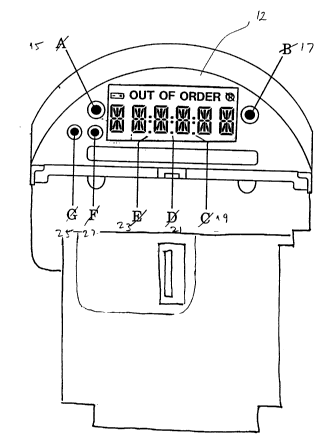
features of a parkin~ meter 10 accordin~to a preferred embodiment invention.
The meter includes a housin~ 12, a display 14 disposed at the upper end of the
5 housin~ in conventional fashion, a coin slot 16 for receivin~ coins or tokens,and an optional card slot 18 for receiving and communicatin~ with a smartcard
20. A coin chute 22, shown in FIGURE 28, is secured within the housing and
provides a vertical passa~eway between the coin slot and a conventional coin
receptacle ~not shown) also disposed within the housin~.
10Display 14 includes a main display 24 havin~ a six-character/96 segment
LCD display for displayin~ Purchased Time Remainin~ when the meter is in use,
a scrollin~ messa~e when the meter is not in use and other such messages.
The display can also be used to alternatively scroll a message and display
purchase time. The display also includes a left hand LED 26, a right hand
15LED 28, an "Out of Order~ indicator 30, an ~Invalid Coin Indicator~ 32, and a
~Low Battery Indicator~ 34. The display also includes inr~ared transmit and
receive mode indicators 36 and 38, respectively, to indicate when the meter is
in infrared transmittin~ and receivin~ modes, respectively. One of the
challen~es associated with providin~ an parkin~ meter electronic display havin~
20 so many indicators is maintainin~ power consumption to a minimum. The
manner in which the present invention achieves this objective is described later.
The information displayed on display 14 may be varied accordin~ a
computer program loaded into the meter. After a user has deposited coins or
tokens or inserted a Slll&l Icard into the meter, the meter will display the amount
25 of time remainin~. The time may be updated at one second intervals for the
balance of the unexpired time. Aller"ali~ely, the time may be displayed for
only a few seconds and then display a series of bars. When time has expired,
the display may be blank or may display a scrollin~ messa~e, perhaps in the
form of advertisin~.
217~28
The parkin~ meter of the present invention is capable of communicating
with an external computer (not shown) by means of an RF probe 40 connected
to the external computer. The e~l~r"al computer may be any conventional,
commercially available, portable computer. The RF probe is used to download
5 computer pro~rams and/or data into and/or upload data from the meter. In
accordance with one of the many aspects of the present invention, the coin
detection circuitry of the present invention serves the dual role of detectin~ the
presence of and measurin~ coins in the coin chute and effectin~ RF
communications. To effect RF communicalior,s, the RF probe is simply inserted
10 into the coin slot. This aspect of the invention is described in more detail later.
The meter may also include a conventional infrared transmitter/receiver 42.
The meter is provided with a ~eneric operatin~ system which reads
specific re~isters stored in non-volatile memory to determine its operating
parameters. The para" ,aler:" for example, may specify the messa~es which are
15 to be displayed under certain circl""slances, the rates to be charged and the intervals within which those rates apply, etc.
FIGURE 2 illusl~dles the three basic states of the meter in the form of a
3-state machine having an IDLE state in which there is no time purchased, a
PURCHASED state in which purchased time remains and a GRACE state which
20 permits some non-purchased time before a violation messa~e is issued. The
IDLE state is entered from system reset and a default messa~e is output to the
display. The IDLE state transitions to the PURCHASED state when ENABLED
and CREDITS fla~s have been applied. The purchased time is output to the
display. The meter remains in the PURCHASED state while credits are applied
25 to the account and transitions to the GRACE state when the purchased time
expires. The GRACE state reverts to the PURCHASED state when additional
credits are applied or to the IDLE state when the GRACE period expires. The
GRACE and PURCHASED states exit to the IDLE state whenever the ENABLED
fla~ becomes false.
2173428
- 10-
Reference will now be made to FIGURE 3 which is a block dia~ram
illustrating the major components the present invention. The meter is
comprised of aforementioned display section 14, including backlight and LEDs
44, a slave controller 50, a master controller 52, memory means in the form of
an EEPROM 54, a power supply/switching regulator circuit 56, a battery pack
58, a mixed signal Application Specific Integrated Circuit (ASIC) 60, a proximity
and RF communications interrdce 62, proximity detector coils and bridge coils
64, and a Smartcard detection and interface circuit 66.
Generally, the ASIC provides coin disc,i,.,inalion functions and, more
specifically, converts analog si~nals output by the detectors to digital signalswhich are then delivered to the master controller. The coin discrimination
aspects of the ASIC are described and claimed in the Pale"lee's Canadian-
Patent Application Serial Number 2,113,492 filed on January 14, 1994 and,
accordingly, it will not be described herein in detail except where necessary tounderstand other components of the present invention.
It will be noted from FIGURE 3 that a first crystal oscillator 68 is
connected to the ASIC. The output of oscillator 68 provides the clock signal
for the master controller as well as for the ASIC. It will also be noted that a
second oscillator 70 is connected to and provides clock signals to the slave
controller 50. Slave controller 50 incll~des an internal LCD driver and MASK
ROM. Master controller 52 includes an internal UART, an 8-channel analog-to-
digital converter ~ADC) and MASK ROM.
The Processing Section
One aspect of the present invention partitions processing functionality
between two controllers 50 and 52. The purpose of this partitioning is to
separate quiescent state functions and active state functions in order to
opli",i~a power supply requirements. To that end, the power supply system
provides a very low current -3.3 volt supply to support the quiescent state
functions and a high current -5 volt supply to support active state functions.
~1734~8
- 11 -
The quiescent mode functions are allocated to a very low power (4~A
Active) ~bit microcontroller, i.e. to slave microcontroller 50. An appropriate
commercially available device is an OKI MSM64164GSK microcontroller, which
is powered on the low current -3.3 volt power supply. The specific functions
allocated to this device include drivin~ the display, coin proximity detector and
mana~ement, Smartcard deteclion and manaç,e",e"t, power mana~ement and
battery detection, configurable bit port control lines, Watchdo~ Timer
maintenance as well as controllin~ the various displays includin~ the main
triplex LCD display driver, an auxiliary 4 se~ment static LCD driver, LED
operation, real time clock and meter time mana~ement.
The Active mode functions are allocated to an 8-bit processor, master
controller 52. An appropriate commercially available device is the Texas
Instruments TMS370C350FNA. The master controller operates from the -5.0
volt supply labelled VSS in the circuit dia~rams described later. Active mode
operations executed by master controller 52 include Coin Discrimination,
Battery Level Monitorin~, User Communications, communications with
microcontroller 50, Smartcard Interface communications, coin chute block
monitorin~, bootload and Pro~ram Memory Mana~ement and System
Dia~nostics.
Master controller 52 is preferably provided with an internal mask ROM
to store bootloader code to control system reset. Memory is partitioned off of
the ",icrocontrollers in order render the systems as ~eneric and flexible as
possible. To that end, the system includes a memory device in the form an
EEPROM.
q~ie~csnt State Functions
Main Triplex LCD Display Driver
With reference to FIGURES 4 and 5, slave controller 50 is provided with
a triplex mode LCD driver. A pinout, L0...L33, is allocated to provide a re~ular30 routin~ pattern for the LCD panel when the slave controller 50 is positioned
2173428
- 12 -
beneath the front LCD ~lass. Slave controller 50 is provided with an internal
char~e pump which converts the -3.3 volt (nominal) power supply into an
appropriate -4.5 volt LCD drive waveform and, in this way, is able to provide
the necessary volta~e to drive the display while the power supply provides the
5 low volta~e level.
Auxiliary 4Se~ment Static LCD Driver
Auxiliary static mode LCD frontplane drivers are impiemented with bit
ports from bit port 2 on slave controller 50 and a static backplane is ~eneratedvia the buzzer output confi~ured as a bit port. Ports 1, 2, 3 and 4 on slave
10 controller 50 have built in level translation circuitry that allow them to operate
in two modes. When the ne~ative power supply VSS2 (OKIVSS2) and VSS
(VSSINT) are at -3.3 volts, the bit ports operate with O volts as a logic high and
-3.3 volts as a logic low. When the power supply VSS (labelled VSSINT in the
drawin~s) is brou~ht to -5.0 volts, the bit ports operdte with O volts as a lo~ic
15 hi~h and -5.0 volts as a lo~ic low. This ~uarantees proper interface between
the two processors even thou~h they run on a split power supply system.
The effect of the volta~e swin~ transition of the frontplane signals for
the static display will be minimal. The buzzer output does not have the
translation circuitry and always operates between O volts and -3.3 volts
20 (VSS2). When static se~ments are ON and the frontplane and backplane
signals are out of phase, a chan~e to active mode results in a sli~htly lar~er
avera~e power being delivered to the LCD se~ments. When static se~ enls
are OFF and frontplane and backrlane si~nals are in phase, a change to active
mode will result in a sli~ht increase in avera~e power delivered to the LCD
25 se~ment on one half of the se~ment update cycle, but not enough to turn the
se~ment ON.
Coin Proximity Deteolor and Mana~e ,-ont
An electronic proximity detector, described later, provides an output
indicative of the presence of an object in the coin chute. Slave controller 50
2173~28
- 13 -
monitors the output of the proxi-,-ily detector at predetermined, software
selectable intervals of 32 or 64 Hz. While the output could be monitored
continuously, doin~ so would considerably increase enerqy consumption and
would not provide better monitorin~ of the detector. A low level detector
5 output indicates no activity in the coin chute and, therefore, no further action
need be taken. Conversely, a hi~h level output indicates the presence of an
object. Slave controller 50 responds to the latter situation by initiating a
master controller 52 wakeup sequence described later. Master controller 52
subsequently determines whether a coin has entered the chute, the chute has
10 been obstructed or an RF probe has been inserted into the chute. These
functions are described more fully later.
Smartcard Detection
The smartcard feature is optional. However, the apparatus is provided
15 with the circuitry necessary to monitor and communicate with a smartcard via
the smartcard interface shown in FIGURE 10. When the smartcard option is
installed, a bit port on slave controller 50 is dedicated to the periodic samplinq
and detection for smartcard insertion. A normally open switch is located on the
smartcard interface. At a period of 64Hz, the lo~ic state of a CARDINN signal
20 is sampled ~see FIGURE 4). A hi~h level si~nal indicates that no card is present
and no action is taken. A low level si~nal indicates the presence of a card
which causes slave controller 50 to initiate the master controller wakeup
sequence.
Real Time Clock and Meter Time Mana~e ,.~.,l
Slave controller 50 contains an internal time base counter for ~enerdlin~
a real time clock and meter time mana~ement. The time base counter is based
upon a 32.768 kHz crystal oscillator 70. An external trimmer capacitor 80 (see
FIGURE 4) is provided to allow a factory trim of the initial oscillator set point.
Durinq quiescent operation, slave controller 50 code executes from the
~173~8
- 14 -
32.768 kHz crystal oscillator. This maintains a low power and slow, but
sufficient, mode of operalion. Durin~ meter wakeup sequences, slave controller
50 starts a secondary RC oscillator formed with an inter~,al capacilor and
external resistor 82. The controller code then switches to the faster clock
5 oscillator source and operates approximately 12 times faster.
Power Mana~ement and Battery Detec~io~-
Slave controller 50 ~enerates the required conditional control si~nals to
turn the -5.0 volt power supply system ON and OFF. The -5.0 volt power
10 supply system is turned ON when a control si~nal HSTPWRN (FIGURE 4 and
9) is set low. The -5.0 volts power supply system is turned OFF when this
control si~nal is hi~h. The si~nal HSTPWRN si~nal is enabled and the -5.0 volt
supply system turned ON when one or more of the followin~ events occur:
(a) a preset alarm timer expires, (b) a proxir"il~/ detector trip occurs, (c~ a
15 smartcard detection occurs, (d) a watchdo~ timer fault has occurred, or (e) asystem reset sequence is detected. The si~nal HSTPWRN is disabled and the
-5.0 volt supply system is turned OFF only when the followin~ events occur:
(a) master controller 52 requests a power down sequence, (b) the watchdog
timer has not been serviced within a predetermined time interval, or (c) the
20 battery has been removed from the unit.
When the HSTPWRN si~nal is activated, slave controller 50 begins a
sequence that depends upon the successful servicin~ of a watchdo~ timer
interface described later. Slave controller 50 be~ins a recovery sequence if thewatchdo~ timer has not been serviced after the HSTPWRN si~nal has been
25 activated, indicatin~ a failure of either the -5 volt power supply or the active
processor section. The recovery sequence involves deassertin~ the HSTPWRN
si~nal for a short period of time and then reasse,tin~ the si~nal. If the resultof this sequence is another failure to service the watchdo~ timer, slave
controller 50 executes a meter shutdown sequence similar to that when the
217~428
- 15-
battery is removed from the unit. Recovery from this state can only be
achieved throu~h a full, manual meter reset.
With reference to FIGURE 4, battery detection is provided by a simple
level translation circuit formed by resistor 84, diode 86, resistor 88 and resistor
5 90 (see FIGURE 4). When a battery is present, resistor 84 is pulled to VBAT,
diode 86 is forward biased, and a si~nal BATTERYN is pulled to approximately
0 volts via a volta~e divider ~r",ed by resistors 88 and 90. When the battery
is removed, the voltage on the resistive divider of resistors 88 and 90 is also
removed and BATTERYN collapses to the VSS2 power supply rail. When the
10 BATTERYN signal has collapsed to VSS2, slave controller 50 disables the
HSTPWRN si~nal, turns OFF LED0 and LED1 (if they are ON), shown in
FIGURE 4, and disables the proximity detector. Functions are not re-enabled
until the battery has been restored to the unit.
Confi~urable Bit Port Control Lines
The slave controller controls four auxiliary static display frontplane
si~nals which can be alternately confi~ured as read/write bit ports for use as
control or monitoring lines.
Watchdo~ Timer
A watchdo~ timer is provided across the controllers. This means that the
functional timer resides in slave controller 50 and a watchdo~ timer servicin~
routine is run on microcontroller 52. An interface to service the watchdo~
timer is attained over a master controller 52 to slave controller 50 serial
peripheral interface 72. The watchdo~ timer is active only when active mode
functions have been activated by turnin~ the -5 volts power supply ON by
assertin~ the HSTPWRN si~nal. The watchdo~ timer is provided to encompass
details such as the detection of pro~ram memory errors, system failures, and
system dia~--oslics. If, durin~ an active period, the watchdo~ timer is not
serviced within a four second interval, a watchdo~ timer power deactivation
2~7~28
- 16 -
sequence is tri~gered as indicated earlier and an error recovery sequence is
initiated (described later with reference to Bootloader and Pro~ram Memory
Mana~ement).
5 Master co,-lf~ r 52 and Active State Functions
The basic mode of operation of master controller 52 will now be
described with reference to FIGURE 6. As previously mentioned, active mode
functions are the responsibility of master controller 52. Master controller 52
operates from the -5.0 volt supply labelled VSS. This power supply is directly
10 controlled by the slave controller 50 bit port HSTPWRN. System clock HSTCLK
and processor reset HS I ~S l N (open drain) are ~enerated by the coin
discrimination ASIC.
When HSTPWRN is activated, the VSS power supply be~ins to swin~
from zero volts towards -5.0 volts. The H5 1 ~S I N si~nal is held at the ne~ative
15 rail by the coin discrimination ASIC as VSS be~ins to ramp down. Crystal
oscillator 68 on the coin discrimination ASIC be~ins to run at about -3.0 volts
and the resultant clock si~nal is buffered and sent to master controller 52 as
the si~nal HSTCLK. When the volta~e reaches -4.5 volts, a volta~e comparator
within the ASIC releases a 500~S delay counter. When the delay counter
20 expires, the reset si~nal HSTRSTN rele~ses and master controller 52 begins to execute.
The power down sequence for master controller 52 is controlled for the
most part by lo~ic in the coin discrimination ASIC as discussed earlier with
reference to Power Mana~ement and Battery Detection. As HSTPWRN is
25 deasse, led, the VSS supply be~ins to drop potential. A co~pardLor within theASIC detects a drop below 4.5 volts. H5l~5lr~J is inslanlly asserted and
master controller 52 is powered down in a controlled fashion.
The memory map for master controller 52 has been allocated to provide
a secure mask ROM bootload seclion and confi~urable pro~ram personality
30 code. All exler"al access address decode is provided by address decode lo~ic
~173~28
contained in master controller 52 confi~ured in microcontroller mode with
Function A expansion. This mode provides an active a low write enable si~nal
RWN, an active low pro~ram memory chip select si~nal CSH1N and an active
low peripheral select si~nal CSPFN. One additional control line for address
5 decode is provided by the coin discri",inalion ASIC, and this is the program
memory output enable si~nal PMEMENN which is a decoded combination of the
RWN, CSH1N and HSTRSTN si~nals. The active mode functions will now be
described briefly.
Coin Discrimination
The coin discrimination functionality provided by master controller 52
encornrasses mana~ement of the mixed si~nal coin discrimination ASIC
resources, samplin~ of the resultant analo~ si~nals, and execution of coin
discrimination al~orithms (includin~ brid~e balance). Master controller 52
15 interfaces to the mixed si~nal ASIC, U37 via a ~bit wide data bus labelled
D[O. .3~, and accesses are qualified by the address decode si~nal CSPFN and the
two address least si~nificant bits (Isb's) AO and A1.
The mixed si~nal ASIC provides an analo~ interface to master controller
52 via a built-in 8-bit A/D converter. A si~nal MAGOUT is a linear O to 5 volt
20 si~nal which is linearly proportional to the difference si~nal as detected across
a coin discrimination brid~e described later. This si~nal is sampled on channel
7 of the master controller 52 A/D converter. An output si~nal PDETOUT is a
CMOS di~ital si~nal from the mixed si~nal ASIC which is low pass filtered to
~enerate a linear O to 5 volt si~nal. This filtered si~nal indicates the phase
25 relationship between a brid~e input si~nal BRDDRV and a bridge output
difference si~nal. The system ~enerales two of these filtered signals from the
same di~ital output, allowin~ the system to choose the optimal step response
and ripple characteristics of the two. A first si~nal PDETF1 is filtered by the
RC low pass combination of R9 and C2 and is intended for the lower frequency
30 ran~es where phase accuracy tends to be a bit better but filtered phase
~173~28
- 18 -
detector step response is poor because of the lower frequencies. Signal
PDETF1 interfaces to master controller 52 via A/D channel 6. A second signal
PDETF2 is filtered by the RC low pass combination of R10 and C3 and is
intended for the hi~her frequency ran~es. PDETF2 interfaces to master
5 controller 52 via A/D channel 5.
l~lt~ Level Monitorin~
Master controller 52 monitors the actively loaded battery condition via
a si~nal VBATCHK on channel 4 of the A/D converter. VBATCHK is derived
from a resistive divider formed by resistors 100 and 102 which provides a ratio
of the varyin~ battery volta~e VBAT and the static -5 volt supply volta~e VSS.
In ~eneral, sensitivity is about 66mV of battery volta~e per A/D step. Low
battery thresholds are set in software and vary with different battery
confi~urations .
User Communications
As previously mentioned, master controller 52 contains an inte~ral UART
which is used for user communications. A si~nal SDOUT is the 5 volt UART
transmit signal and a si~nal CDIPSDIN is the 5 volt UART receive si~nal.
CDIPSDIN is also connected to slave controller 50 and is alternatively used for
proximity detection.
The proximity deteclor power supply increases from the -3.3 volt supply
to the -5 volt supply when master controller 52 is powered to allow the
CDIPSDIN si~nal to interface directly with the master controller 52 UART.
The rf communications link is a half duplex link, with master controller
52 as the initiator. To communicate, master controller 52 first disables the
coin detect operation of the proximity detector. It does this by resettin~ a
PROXENP si~nal, which stops the coin detection algorithm in slave controller
50. Serial data is then transr-,illed via SDOUT and is used to ~ate the
proximity detector oscillator ON and OFF. This is accomplished by turnin~ ON
2173428
- 19-
and OFF the biasin~ volta~e to the proximity detector circuit via transistor 104(FIGURE 8). The result is a modulated pulse stream which can then be
recovered with an appropriate receiver confi~uration.
Generally speakin~, there is a communications protocol which allows the
5 meter to ask for and then receive specific packets of information. Once a
transmit packet has been sent, master controller 52 initiates a listen mode in
which master controller transmissions stop and the proximity detector becon ,es
a receiver.
Slave controller 50 Communications
Interface between controllers 50 and 32 is achieved with a serial
peripheral interface, a function contained on both processors. Master controller52 provides the master clock, labelled SCLK, for this interface, and slave
controller 50 is a slave. The frequency of SCLK has been chosen at around
15 100 kHz to accG, - " "odate the maximum transfer frequency of slave controller
50.
Serial data is transmitted from master controller 52 to slave controller 50
on a si~nal SIN and received from slave controller 50 on a signal SOUT. A
si~nal SPR is ~enerated by slave controller 50 to indicate that it is ready for the
20 next byte transfer and this si~nal is connected to interrupt 3 on master
controller 52 so that it may be polled or interrupt driven.
Card Interface Communications
Detection of a smartcard is provided by slave controller 50, as already
25 mentioned; however, after system powerup, all communications with the
smartcard interface are provided by master controller 52. S..,arlcard interface
functions are provided on a dau~hterboard confi~uration which contains a
serially loaded 8-bit control re~ister. Interface to this unit is provided by bit
software controlled ports to provide the correct protocols. A si~nal CARDINN
is normally pulled hi~h by resistor 110 (see FIGURE 10). Insertion of a card
217~4~8
- 20-
closes a normally open contact and pulls CARDINN to VSSINT. The slave
controller 50 detects the presence of the card and powers up master controller
52. As the -5 volt supply turns on, VSSINT increases from -3.3 volts to -5
volts for interface with master controller 52. Interface data is transmitted on
5 a bit port labelled CARDDIN and cloc~ed with a si~nal SERCLK. 8-bits are
written in this manner and then loaded into the control re~ister with a si~nal
PARCLK. Data is shifted out from the card interface to master controller 52 via
a CARDDOUT si~nal.
Chute Block Monitorin~
A bit port pair on master controller 52 are dedicated to allow an IR LED
and IR detector combination to indicate the presence of non-metallic jams in thecoin chute.
Bootload and Pro~ram Memory Mana~ement
As indicated earlier, master controller 52 contains mask ROM and can
execute from both internal mask ROM pro~ram memory and external EEPROM
based mask ROM memory. The internal mask ROM program memory is
dedicated to bootload, pro~ram download and pro~ram memory mana~ement.
After reset, master controller 52 jumps to the internal mask ROM
pro~ram memory. A test of the external pro~ram memory indicates whether
or not a location desi~nated as the pro~ram valid byte has the proper value.
If it has, master controller 52 immediately jumps to execute external pro~ra,.,
memory. If the byte is not valid, master controller 52 initiates a download
sequence. No servicin~ of the watchdo~ is done if no valid communications are
established and master controller 52 enters an error recovery sequence and
then an out of service mode.
If the pro~ram valid byte is correct but the pro~ram memory has been
corrupted, master controller 52 will be~in to execute in e~l~r"al pro~ram
217342~
-21-
memory, fail to service the watchdo~ timer interface, and enter the error
recovery sequence.
The error recovery sequence, which executes whenever a watchdo~
timer interrupt sequence occurs, marks a pro~ram valid byte as invalid. When
this byte is detected as invalid, the bootloader code is activated, and the
pro~ram alle-npl5 to initiate communications for a pro~ram download. No
servicin~ of the watchdo~ timer is done durin~ this initial attempt at download,which means that if no communications device is present, the meter out of
service mode is enlered. This effectively shuts down the meter. Exit from this
10 mode is possible only by an exler"al system reset.
Proqram memory mana~ement software is contained in the master
controller 52 mask ROM. This pro~ram supports EEPROM pa~e write and-
software controlled write enable and disable sequences (Catalyst 28C256 and
similar devices). During write sequences to pro~ram memory, the mask ROM
portion of the program memory contains the proper routines to transfer data
buffered in master controller 52 internal SRAM into the external EEPROM. The
master controller executes out of the internal mask ROM pro~ram memory for
this transfer sequence because the EEPROM is taken temporarily out of service
by the write operation. This pro~ram memory manaqement hook is available
to both the internal mask ROM boolloader code as well as the externally
accessed EEPROM user pro~rams.
System Dia~..cslics
Master controller 52 iS available to execute limited system level
dia~nostics, however, these need not be described herein inasmuch as they do
not form part of the invention.
Proximity Detector
The present invention provides a simple and effective proximity detector
30 which overcomes many of the disadvanta~es of the prior art discussed earlier.
~173~2~
- 22 -
In ~eneral, the proximity detector utilizes two coils, one in the collector and the
other in the base of a simple common-emitter amplifier. The detector is based
on the basic principle that stable operation depends very stron~ly upon proper
ali~nment and spacin~ of the two coils. Any disturbance, even minor ones, will
cause the oscillations to cease completely. When the interference is removed,
the oscillator resl~. Is reliably.
FIGURE 8 illuslrales the ele~ant simplicity of this circuit. Two coils are
wound on 14 mm by 8 mm bobbins located directly opposite each other on
either side of a coin slot. With no coin or metal object in the chute, the circuit
oscillates at about 400 kHz with an amplitude of 3 volts peak-to-peak. Even
a false aluminum coin the size of a dime will cause the oscillator to stop,
reducin~ the output to zero. The Gscilla~or is followed by a simple envelope
detector and level shifter as required by the controller.
The proximity detector is implemented with an inductively coupled
oscillator. The detector circuit consists of a tuned circuit which is formed by
the combination of capacitor 120, a 1 .8nF capacitor in parallel with one air core
bobbin 122 at the base of transistor 124, and capacilor 126, a 3.3nF capacitor
in parallel with another identical air core bobbin 128 at the collector of
transistor 130 (specified inductance of the air core bobbins is approximately
68~JH or 100 turns of 28 ~auge wire). For the oscillation to start, a biasin~
volta~e must be applied to resistor 132, allowin~ transistor 130 to turn ON.
From there, out of phase inductive couplin~ between the two air core bobbins
provides feedback to start and maintain the oscillation. The base and collector
circuits are sli~htly detuned to enhance the ability to stop the oscillator by
breakin~ the inductive couplin~ between the bobbins ~i.e. by blockin~ the
physical path with metal).
The operation of the proximity detector circuit as a coin detection system
can be described as follows. At a software selectable period of either 32 Hz
or 64 Hz, slave controller 50 samples the PROXENP si~nal. If the si~nal is low,
the proximity detector is disabled and no further action is taken. If this si~nal
217342~
- 23-
is hi~h, the proximity detector is enabled. Then, if the BATTERYN si~nal is
hi~h, indicatin~ that a battery is installed, output si~nal CDOP is set low,
turnin~ transistor 132 ON and biasin~ the proximity detector oscillator.
On the next processor cycle (approxin,alely 60/~S later), slave controller
5 50 samples the CDIPSDIN si~nal. If the CDIPSDIN si~nal is low, the proximity
oscillator is operational and the rectified and filtered volta~e ~enerated by the
combination of capacitor 138, diode 136, and resistor 140 is enough to turn
transistor 142 ON. No metal is blockin~ the proximity bobbins. If the
CDIPSDIN si~nal is hi~h, the oscillator did not start and presumably somethiny
10 metallic (i.e. a coin) is blockin~ the proximity bobbins. The slave controller 50
then starts the master controller 52 wakeup sequence.
Re~ardless of the result, on the next processor cycle, slave controller 50
resets the CDOP si~nal low which turns the proximity detector oscillator OFF.
This oscillator active period is approximately 1 20/JS lon~ and repeats at the
15 software selected repetition period.
2173~28
- 24-
RF Commufi!cstio.)s
It has been found that, advanta~eously, the proximity detect circuit can
serve an additional role without modification. That role is to effect RF
communications with a suitable RF probe described below.
RF Prob~
The RF probe consists of a circuit board sul,sl-ale, 1/16" thick, 0.75"
hi~h, and 3.0 in len~th. The thickness and hei~ht determine the minimum coin
slot dimensions that will allow the probe to be inserted into. Only about 1.5"
of the circuit board suLsl,ale is inserted into the coin slot, and a notch in the
substrate is provided to allow the coin slot to drop into when the probe is
inserted in throu~h the coin slot. The inserted portion of the RF probe containscopper clad substrate, and a hollowed out section of the circuit board which
has a ti~htly wound coil (L1) inserted into the hollowed out section. The
copper clad portion of the circuit board serves to interrupt the meter proximitycircuit as it is inserted. The probe continues to be inserted until the coin slot
drops into the notch described above. When the probe has positioned to the
slot position, the coil (L1) is now perfectly ali~ned between the proximity
detector coils of the meter.
When the meter receives the coin interrupt, ~enerated by the insertion
of the probe, it will first try and measure the physical properties of an objectthat would normally drop down the coin chute and into the balanced brid~e coil
arran~ement. With the absence of any object, the meter under pro~ram control
will transmit a communications packet by sendin~ serial data out (SDOUT) from
the 8 bit microcontroller. The SDOUT serial data signal will alternatively turn
on and off transistor 104 (fi~ure 5) which in turn will activate the proximity
oscillator circuit, which will immediately be~in to oscillate at 400Khz. In thisfashion, the meter is modulatin~ the data. Oscillation will take place because
the coil (L1) of the RF probe appears transparent to the p~oxil-~ily detector
when L1 is not terminated by a low impedance. The modulated si~nals from
the meter are coupled to coil (L1) on the RF probe, and that same received
2173~8
- 25 -
signal is coupled throu~h capacitor (C5) to a common emitter amplifier circuit
consistin~ of transistor Q1, and resistors R2, R3, R7, and R8. The amplified
400 Khz si~nal is coupled throu~h capacitor C3 where the si~nal is filtered and
stripped of it's modulation frequency by wave shaper components D1, C4. At
5 this time the serial data has been demodulated, and is level translated to a TTL
level and inverted by transistor Q2 and resistors R5, R6 and R4. The serial TTL
level data stream enters pin 2 of IC (U1) which is a MAX233ACWP TTL to
RS232C level converter IC. The serial data is inverted, and level shifted to theRS232 ( + /- 12V) levels on pin 5 and sent to the computer or other device that
10 will receive and interpret the serial data.
When the receivin~ computin~ device receives the si~nal from the meter
it will send the serial RS232 serial data to pin 4 of IC (U1) which level shifts it
and inverts it to TTL levels, on pin 3. The serial data on pin 3 of IC(U1) is
passed to one input of a lo~ical two input OR ~ate, U2D. The aller"dlin~ high
15 and low signals of the serial data stream arrivin~ on the input pin to this ~ate
will alternately force the ~ate U2D to break into oscillation at a frequency
determined by the reactive components C6, C7 and the probe coil L1. The
oscillation frequency is approx. 400kHz. The modulated serial data signal is
coupled across to the meter throu~h the proximity detector coils L2 and L1.
20 The proximity detector oscillator is disabled while the remote computer is
transmittin~, thereby makin~ the communicalio.)s system a half duplex one.
The modulated serial data stream is coupled throu~h capacitor C4 and in an
identical fashion as done on the RF probe, it is stripped of the modulation and
wave shaped by components 136 (Fi~. 8) and capacitor 138. The serial data
25 si~nal is then level shifted and inverted by transistor 142. The serial data
stream is then passed to the 8 bit ",icrocG,-,puter for interpretation by the onboard UART.
~7~428
- 26-
Pow~r Supply Circuit
The Power Supply System consists of a dual switchin~ combination
which provides a low current, qu escent volta~e and a hi~her current active
state volta~e.
Low power quiescent mode runs continuously and is desi~ned to have
an active quiescent current of less than 20~A while maintainin~ a nominal
supply volta~e of 3.4 volts. Maximum supply current from the low quiescent
mode supply is in the ran~e of 5 - 10mA. Typical load demand on this supply
is in the ran~e of 201~Ah. The hi~her current active state supply is desi~ned tomaintain a supply volta~e of 5 volts (+5%) while sourcin~ up to 50mA of
current.
The supply system is comprised of three subsections: an oscillator
subsection, a comparator subsection and a volta~e inverter subsection. The
remainder of this section provides a detailed operational description of each ofthese subsections.
The oscillator section is realized with a 4093 CMOS Schmitt tri~ered
nand ~ate. The nand ~ates are confi~ured as two pairs, one formin~ an
oscillator for the low quiescent current power supply and the second formin~
an oscillator for the hi~her current active state supply.
The pairs of two nand qates are confiqured in a manner which results in
an astable multivibrator circuit. Special characteristics of this astable include
the followinq. An ON/OFF switch is used for volta~e requlation. A latching
mechanism provided by feed~ack eliminates the possibility of short pulses at
the end of a pulse train which could reduce power supply erriciency. In
addition, the astable for the hi~her power supply includes transistor Q23 which
ensures the consislent period of startinq pulses in a pulse train and transistorQ20 which reduces the frequency of operation for a battery condition of less
than a predefined value.
The comparator section consists of a low quiescent current comparator,
- 30 bandgap reference and volta~e divider resistors. One comparator is used for
2~7~28
- 27 -
the low quiescent current supply while three are used for the active state
supply.
The comparator system for the low quiescent state supply is fairly
simple. Volta~e divider R19 and R20 provides a reference volta~e (labelled
VREF2) of approximately +0.9 volts. Re~ulation resistive divider R22 and R21
is referenced from the band~ap + 1.8 volts and the inverter qenerated volta~e
of -3.4 volts. When the ne~ative volta~e threshold of nominally -3.4 volts is
crossed, the output volta~e from the re~ulation divider ~oes below 0.9 volts
and the output of the comparator V3REGP ~oes hi~h. This disables the astable
multivibrator oscillator (output 3VOSC) and stops the inverter. The oscillator
stays disabled until the volta~e at the output of the inverter rises above the
value preset by the re~ulator resistive divider.
The comparator section for the active state supply operates in a similar
manner. VREF2 is compared aqainst the output of requlation resistive dividers
R27 and R28 to maintain nominally -5 volts at the output of the active state
inverter. The output of the active state comparator V5REGN is opposite the
polarity of the V3REGP output since it is fed into a second comparator which
is used as a ~ate for an ON/OFF switch. If transistor Q14 is turned on, output
5VOSCN will enable and disable the active state oscillator as required to
re~ulate the -5 volt power supply. If transistor Q14 is turned off, the active
state oscillator is disabled by the si~nal 5VOSCN (i.e. it is hi~h).
A fourth comparator is used to detect when the battery voltage drops
below 5.5 volts. Resistive divider R42 and R43 provide nominally 1.8 volts
when VBAT is 5.5 volts. Si~nal BATLOWP becomes active and reduces the
frequency of the active state oscillator. This is a requirement of the active
state 5 volt inverter.
The Inverter Subsection includes two inverters. The low quiescent state
inverter consists of transistor Q7, inductor L1, diode D6 and capacitor C10.
The active state inverter is-formed by transistor Q8 and Q11, inductor L2,
~173'128
diode D7 and capacitors C11 and C12. Values for both inverters are chosen
to opti..,i~e efficiency and performance.
Software r`e~C-iplion
The followin~ description describes the architecture of the firmware and
results from partitionin~ the functionality into coherent subpro~ram modules
and the schedulin~ requirements for these funclions
A top level partitionin~, illustrated in FIGURE 11, assi~ns each meter
function to one of the followin~ modules: SERVICE COIN, SERVICE CARD,
SERVICE HOST, MONITOR HEALTH, MAINTAIN TIME/DATE, MANAGE
SCHEDULES, MANAGE DISPLAY, and DISPENSE PARKING TIME. Supportin~
modules required to complete the architecture are: WAKE UP SEQUENCE and
MAIN DISPATCHER
Each of these modules is described below and accompanied by data flow
and state dia~rams where appropriate. The names used for modules, functions
and data items are for desc-ipli~e purposes only. That is, they may not
necessarily coincide with the implementation of the desi~n. The architecture
described here is not a functional specification of the meter of the present
invention, but rather is derived from functional requirements. The architecture
provides a framework into which the software design is implemented.
Wakeup Sequence
The Wakeup Sequence is a pro~ram which executes once per reset and
is entered from startup code after a runtime environment has been established.
Global data structures, such as the Event Table and the Coin Queue, must be
initialized to their idle states, and are done so by calls to initialization functions
in the MAIN DISPATCHER module.
The Watchdo~ Timer Fla~ (WDTF) is then read from the Initial Boot
Pro~ram (IBP) data area, and, if non-zero, it is clealed and the respective event
fla~ is set in the Event Table.
2173428
One initialization routine for each application module is called to perform
any local initialization required. These would include re3ellin~ of state
variables, installation of interrupt vectors and so on.
Finally, the master controller interrupt system is enabled and this program
5 exits to the MAIN DISPATCHER.
Main Dis~,atcher
In each execution cycle, the MAIN DISPATCHER first reads the status
registers of the Multi-Functional Peripheral (MFP) and writes these to the Event10 Table. Usin~ the Event Table and the Coin Queue as input, the pro~ram
dispatcher invokes each application task if its respective event is detected. Itis the responsibility of the individual tasks to clear their respective events.
When all events are serviced, this routine executes the power down sequence.
This module is the centre of schedulin~ activity and is an important
15 component of the architecture, as it defines the priority sche,-,e to be used.
Event mana~ement is locali~ed such that several desiqn approaches to task
schedulin~ can be reali~ed without requirin~ chan~es to other modules.
Essentially, the pro~ram dispalcl.er must retrieve status registers from
the Multi-Functional Peripheral (MFP) and write the individual event fla~s to the
20 Event Table, monitor the Coin Queue for the non-empty status and invoke a
service task for each delecled event. How often these functions are executed
and in what order will define their priority. The followinq is a list of events: SERF Serial Port Event
SECF Second Timer Event
DSPF Display Event
CDIF Card Detect Event
MTRF Meter Event
ALMF Alarm Clock Event
RESF Reset Event
BATF Battery Event
WDTF WatchDoq Timer Event
DAYC Midniqht Counter
COSM Coin Queue Semaphore
~173428
- 30-
Service Host
This pro~ram is invoked via the MAIN DISPATCHER when the SERF
event is asserled. SERVICE HOST provides the means of pro~rammin~ the
meter with replacement software, settin~ its operatin~ parameters and auditin~
5 its data tables. Communication with the external computer is via a half-duplex,
asynchronous serial link. While executin~, all other meter tasks are prevented
from runnin~. In other words, while the exler"al computer is communicating
via the serial input, the meter will not respond to other external inputs.
This pro~ram provides two cate~ories of services. The first provides
10 read and write access to the various internal databases and the second provides
the interface to control functions in other system modules; for example,
settin~ and readin~ the time of day clock.
As menitoned earlier, the proximity detect circuitry forms the physical
link between the external computer and the meter. This circuitry is shared
15 between the SERVICE HOST and SERVICE COIN modules in a mutually
exclusive manner. SERVICE COIN samples the coin chute on a proximity detect
event and, if no measurable coin is found, sets the SERF fla~ and leaves the
proximity circuit idle. The SERF fla~ causes entry to the SERVICE HOST
module from the MAIN DISPATCHER. Communications between the meter and
20 the external computer proceeds as a master-slave relationship, with the meter as the master.
When the external device disconnects, by timeout or by message, the
SERVICE HOST module clears the SERF event fla~ and deasserts the Proximity
Inhibit output si~nal to thereby reactivate the proximity detect circuitry. The
25 SERVICE HOST module then returns to the MAIN DISPATCHER.
Monitor Health
The Monitor Health Module encapsulates functions associated with
determinin~ the operational health of the meter. It provides as output, a fla~
30 which indicates the operational mode of the meter to other modules.
2 173428
- 31 -
Additionally, any required up-to-date status information and lo~ of interestin~
events are recorded for read access by other modules, includin~ the SERVICE
HOST module.
With reference to FIGURE 12, which is a data flow dia~ram, the main
5 entry point of the module is called at periodic intervals to assess the status of
the meter. This mechanism uses a service from the MANAGE SCHEDULES
module. If required by desi~n, a return call to this module, shown as the time
schedule output, pro~rams the time of the next periodic entry.
The MONITOR HEALTH module is also entered from the MAIN
10 DISPATCHER on the occurrence of the RESF (system reset) and BATF (battery
replacement~ to record these events.
As a minimum, two input si~nals are provided to MONITOR HEALTH, as
shown in FIGURE 12 as VBAT and CHUTEBLOCKED. VBAT is a reading of the
power supply volta~e and is accessible via a software function which reads the
15 respective channel of the A/D converter. CHUTEBLOCKED indicates an
obstruction in the coin chute and is provided by a software function which
executes the required sequence to obtain the readin~. Each of these functions
share hardware resources with the SERVICE COIN module. A suitable method
of ensurinq mutual exclusion (for example, maskin~ the coin interrupt or use of
20 a software semaphore) of these resources is necess~ry.
Maintain Time/Date
Mana~ement of the realtime clock is a distributed process. The time and
date ori~qinate from the external computer and are transmitted to the meter via
25 the serial link. Once the meter has set its time and date, the clock proceeds to
run internally and is mana~ed by this module. The Maintain Time/Date module
uses the time of day clock of the MFP as a 24 hour time base and contains the
necessary lo~ic and data stora~qe to maintain the calendar date and
day-of-week.
2173~28
- 32 -
The inputs and outputs of this module are shown in FIGURE 13. The
module contains at least four entry points, one which services the DAYC event
(day rollover count) and is called from the MAIN DISPATCHER and three
functions which are accessib'e to other meter modules: selli"-e unselli"-e and
5 ~ettime. Any other functions needed to translate between time formats used
internally would be included in this module as well.
The settime function is typically called from SERVICE HOST on request
from the external computer. The date information is separated and stored
internally and the time info""alion is used to set the time-of-day clock in the
10 MFP. Alsoatthistime,theDAYCeventcounteriscleared. Finally afterthese
steps are successr-llly completed an internal flaq is set indicatinq that the
realtime clock has been set.
The ~ettime function is a service to any module which wants to
li",eslamp events. One example may be the li",eslampin~ of a sl"a, lcard to
15 indicate its last usa~e. This function determines the validity of the realtime
clock by checkin~ the internal flag and returns an error condition or date/time
as appropriate. The date is retrieved from internal stora~e; the time is retrieved
from the MFP.
Unsettime provides the means of invalidatinq the realtime clock. One use
20 of this function is durin~ a recovery procedure where the state of the realtime
clock is unknown.
The entry point which handles a non-zero DAYC event uses the value of
DAYC to advance the calendar date. The event is cleared before exitin~ to the
MAIN DISPATCHER by writin~ the respective status re~ister on the MFP.
Mana~e Schedules
The Mana~e Schedules module is required to mana~e the schedulin~ of
periodic activities for the meter. Two activities which require schedulin~ are
health checks and the hours of operation for the meter. Any desi~n which
- 30 closely couples this module with the functions it services is an acceptable
2173~28
- 33 -
approach for a small set of activities. For lar~er sets, or where expansion
considerations are an issue, a more appropriate approach would resemble a
client-server model. In the latter approach, MANAGE SCHEDULES would
provide a service for other modules (clients), invokin~ requested functions at
the specified time and without knowled~e of what the function is to do.
From an architectural perspective, the theory of operation of the module
is the same and is represented by the data flow in FIGURE 14. The main entry
point is called from the MAIN DISPATCHER when the ALMF flag is set. The
ALMF event indicates that the previously pro~rammed alarm time matches the
time-of-day clock. A state machine executin~ within the module determines
and invokes the function or functions associ~ted with the alarm time as
indicated in the SCHEDULES database.
Status checks are invoked when required and the functions which
activate/deactivate the DISPENSE METER TIME module are called accordin~ to
the hours of operation. In completin~ the cycle, the system alarm clock is
pro~ran,.ned to its next event in the schedule and the ALMF condition is
cleared.
Service Coin
This module executes the functions required to detect a coin (or other
object) in the chute, measure and discriminate the coin and apply the correct
number of credits to purchased parkin~ time.
The SERVICE COIN module consists of two tasks, MEASURE COIN and
VALIDATE COIN. MEASURE COIN executes in the context of an interrupt
service routine (ISR). VALIDATE COIN executes at the non-interrupt level and
is invoked by the MAIN DISPATCHER. MEASURE COIN is required at the
interrupt level to provide dt:le"--inistic response to proximity events,
independent of which task is executin~ at the non-interrupt level. The interfacebetween MEASURE COIN and VALIDATE COIN is the COIN QUEUE, shown in
2173428
- 34-
FIGURE 15. The COIN QUEUE provides for the latency in schedulin~ the
VALIDATE COIN task.
Each cycle of the MEASURE COIN task, invoked by a proximity event,
posts the measured parameters to the COIN QUEUE. The MAIN DISPATCHER
5 calls VALIDATE COIN when it detects that the COIN QUEUE is non-empty.
VALIDATE COIN then de-queues and processes the event. These operations
are discussed more fully in the followin~ subsections.
Measure Coin
The coin measu~e",ent al~orithm has been described in the Patentee's
afore,.,e"lioned Canadian patentapplication. That algorithm is used as the core
of the Measure Coin ISR.
What remains to be implemented is the interface lo~ic to the COIN
QUEUE and the SERF fla~, both monitored by the MAIN DISPATCHER, and the
15 logic necessary to drive this function via the timer 1 Ed~e Detect Interrupt and
Proximity Inhibit output si~nal.
Timer 1 operales in two modes, pulse width modulated output mode
(PWM) and simple counter mode. Independent of these modes, the peripheral
also provides ed~e detect circuitry as the source of interrupt (proximity detect)
20 and an output bit port which supplies the Proximity Inhibit si~nal. Functionsexist in ROM which provide the necessary interface to the Timer 1 peripheral.
Timer 1 is pro~rammed to simple counter mode when the interrupt
service routine is entered and to PWM mode upon exit.
The Proximity Inhibit output signal is asserted on ISR entry and
25 deasserted on exit unless serial activity is detected.
The COIN QUEUE is posted with a queue element by this function with
each successful measurement of a coin. A queue element contains the
pa,an,eters necess~ry to discriminate the coin via the Coin Tables.
2173428
- 35 -
After each successrul coin measurement, the CHUTEBLOCK input should
be checked for an obstruction in the coin chute and the module MONITOR
HEALTH notiried of an arri--"a~ e result.
MEASURE COIN handles unsuccesstul coin measurements as follows:
1) Unexpected behaviour of the inputs are errors which may be
recorded for dia~nostic purposes.
2) Failure to obtain the coin characlerialics within a predefined time
interval is expected behaviour which indicates serial communications activity.
In the latter case, this function confirms serial port activity, sets the
SERF fla~ and exits the interrupt service routine with the Proximity Inhibit
output asse, led.
Coin Queue
The COIN QUEUE is a FIFO (first-in, first-out) queue of sufficient depth
to handle the number of coins which can be inserted in the worst case cycle
time of the MAIN DISPATCHER. Each queue element is the frequency and
ma~nitude readin~s of a sin~le coin event.
Queue mana~ement is ertecled by three parameters, FILL POINTER,
EMPTY POINTER and COUNTING SEMAPHORE. The FILL POINTER is stepped
around the queue by the MEASURE COIN function with each successrul
readin~. The EMPTY POINTER iâ stepped with each queue element removed
from the queue by the VALIDATE COIN function. The COUNTING
SEMAPHORE is a shared variable incremented by MEASURE COIN when an
element is added to the COIN QUEUE and decremented by VALIDATE COIN
when an ele",enl is removed. Because it is possi~le that the measure coin
function may interrupt VALIDATE COIN procesâin~, enqueuin~ and dequeuing
operations must be uninterruptible to maintain the queue's inte~rity. To ensure
these operations are uninterruptable:
1) the countin~ semaphore is an 8 bit variable in the master controller
internal re~ister file providin~ sin~le CPU instruction ~ccess,
2173428
- 36 -
2) the MAIN DISPATCHER reads the semaphore to determine if the queue
is non-empty, and
3) VALIDATE COIN must decrement the semaphore with the master
controller ~ADD #-1, Rx~ instruction.
Validate Coin
VALIDATE COIN removes and processes elements from the COIN QUEUE
when invoked from the MAIN DISPATCHER. For each element, a
Frequency/Ma~nitude pair, a direct look up in the COIN TABLE deter",;nes the
value of a coin in units of credits. A "miss" in the COIN TABLE and an answer
of zero credits are handled as appropriate to the desi~n. A non-zero answer
from the COIN TABLE is passed directly to the DISPENSE PARKING TIME
module via the function Add Credits. VALIDATE COIN also maintains an Audit
Database for recordin~ the coins deposited in the meter. For auditin~ purposes,
this database is accessible to the SERVICE HOST module.
Service Card
The SERVICE CARD module provides the functionality r,ecessary to
support cash value and non-cash value cards via the smartcard reader.
FIGURE 16 provides a data flow dia~ram for this module. The main entry point
of this module is called from the MAIN DISPATCHER when the CDIF fla~ is set,
indicatin~ a card has been inserted into the card slot. Any requirement to
pa,d"-et,ically drive the response of the meter to a specific card is provided for
in a CARD DATABASE which is accessi~le to SERVICE HOST.
SERVICE CARD aull,e,-ticales, validates and employs any required
encryption/decryption al~orill""s necessary to meet security requirements.
Cash value cards invoke the Add Credits function of DISPENSE PARKING TIME
and may invoke display control functions of MANAGE DISPLAY. Non-cash
value cards may be supported for dia~nostic, supervisory, auditin~ or other
purposes by direct function calls from this module to other meter modules.
~73~2~
- 37 -
Should a card be unexpectedly removed from the reader, the architecture
facilitates realtime responsiveness with the mechanical card-detect si~nal
connected to a master controller external interrupt pin (INT2). This module
executes the purchase of parkinq time from the meter.
Top level partitionin~ is shown in FIGURE 17, which illusl-dtes the data
flows amon~ four key functions and two key data variables. The data is
defined as follows.
The ENABLED fla~ indicates the ability of the meter to accept payment
for purchased time. It is written by the MeterOn and MeterOff functions and
read by MANAGE METER TIME. CREDIT is a buffer which retains an account
balance. It is written by the AddCredits function and may be cleared by the
MeterOn, MeterOff and MANAGE METER TIME functions. The account balance
is credited on each call to AddCredits (typically from SERVICE COIN and
SERVICE CARD). Crediting the account may depend on the ENABLED flag as
15 dictated by desi~n or by pa,arelers in the DPT Database. For example, some
meters may be pro~rammed to accumulate credits while ENABLED is false,
while others may i~nore the request. Once the minimum number of credits are
accumulated, purchased time is dispensed.
The functions MeterOn and MeterOff are provided as input control to
settinq and clearin~ the ENABLED fla~. Aqain, the disposition of the CREDIT
balance at the time of transitionin~ the ENABLED fla~ is a function of the
desi~n.
MANAGE METER TIME is a set of functions which execute a
prepro~fa,..,ned sequence of events in dispensin~ the purchased time. The
25 main entry point is called from the MAIN DISPATCHER when the MTRF fla~ is
detected (indicatin~ meter time expired). In the course of execution, MANAGE
METER TIME controls the alphanumeric and enunciator LCD via calls to
MANAGE DISPLAY.
The functions which make up this module are cooperative and the
30 behaviour of the module at any instant depends on a history of events.
~173428
- 38 -
Therefore, these functions execute as a software state machine. The inputs
of the state machine are CREDIT, ENABLED, MTRF and the DPT Database. The
outputs are its pro~rammin~ of the meter clock and control of the display. The
states are a function of the desi~n and/or parameters stored in the DPT
Database. In fact, how the inputs are interpreted and what is included as
output may be para",elrically driven by the DPT Database, as well. In other
words, the state machine may be pro~ia~r""ed in the lo~ic (software), in the
DPT Database (parametrically done) or some combination of these.
For illustrative pu".oses, a sample impler"enldlion is depicted in the state
dia~ram of FIGURE 2. This implementation is a three-state machine which has
an IDLE state (no time purchasad), a PURCHASED state (purchased time
remains) and a GRACE state (which permits some non-purchased time before
a violation is issued). IDLE state is enlered from system reset and a default
messa~e is output to the display.
IDLE transitions to PURCHASED state when ENABLED and CREDITS
have been applied. The purcl~ased time is output to the display. The meter
remains in PURCHASED state while credits are applied to the account and
transitions to GRACE state when the purchased time expires (indicated by
MTRF).
GRACE state reverts to PURCHASED state when additional credits are
applied or to IDLE state when the GRACE period expires. GRACE and
PURCHASED states exit to IDLE state whenever the ENABLED fla~ becomes
false.
Mana~e Display
Control of the alphanumeric and enunciator LCDs are effected throu~h
library routines within the Mana~e Display module and are provided as a
resource to all meter modules. FIGURE 18 illuslralcs a minimal desi~n
requirement and it is expected that additional functions will be specified by the
desi~n.
217~2~
- 39 -
The SWITCH DISPLAY entry point from the MAIN DISPATCHER linvoked
when the period of the current display has expired) provides for displayin~ a
default messa~e (when there is no other display defined) or for imple..,enlin~
queued output if a requirement for this exists. The DISPLAY QUEUE is included
in FIGURE 18 for this requirement and if queued output is not required, the
DISPLAY QUEUE has zero depth. As specified here, the architecture provides
control of the display to one or many processas Imodules) at one time. The
key point is that display require"-6l-ts are not an architectural issue but a
function of the desi~n concept and are consl,ained only by the MFP's display
1 0 capability.
Initial Boot ROM
The Initial Boot ROM is the system residin~ in master controller mask
ROM which provides initial boot and reset functions for the meter. The
following descriplion describes the Reset module, the Boot Loader, the runtime
environment established by the Reset Module and is inherited by the application
pro~ram and the callable functions which exist in the mask ROM.
RQsQt Module
This module consists of the lo~ic and data requirements to launch the
execution of an applicatiG" pro~ram. It is entered immediately upon reset of
the master controller. The Reset Module is responsible for initializin~ system
speciric hardware, determinin~ the existence of application software (executin~
the boot loader, if necessary) and establishin~ the runtime environment before
passin~ control to the app! ~tion pro~ram.
The desi~n of this module is represel~led in the flow chart of FIGURE 19
and desc,ibed as follovss. The Reset Module first pro~,r~,..s the master
controller exler..al ports as the system bus interface, enablin~ 16 address lines,
8 data lines, the read/write !ine and two chip select lines. Next, the TIMER1
30 module is initialized to capture proximity circuit events and a handshake is
2173~28
- 40 -
performed with the MFP, enablin~ communications with this device via the
Serial Peripheral Interface (SPI).
A TIMER1 peripheral is then checked to deter,-,ine if the master controller
reset was caused by a proximity event. If this is the case, and an application
5 pro~ram exists in EEPROM memory, control is pa-ssed to the application via the procedure indicated at the bottom of the flow chart.
Failin~ this test, if the WDTF (watchdo~ timer flag) is set, the existin~
application pro~ram is cleared (by zeroin~ the Application Version Number in
EEPROM). The module then passes control to the applicalion if one is installed.
10 Otherwise, it disables the proximity detect lo~ic (enablin~ Serial
Communications Interface (SCI) communications) and enters the boot loader to
obtain a software download.
If the boot loader is unsuccessful in capturin~ the download, the
proximity circuit is re-enabled and the master controller is powered down.
15 When the communications probe is reinserted in the mouth of the coin chute,
the master controller is powered and execution restarts at the Reset Module's
entry point.
A successful download is installed by writin~ the point address and
version number of the application to the EEPROM. The proximity circuit is
20 enabled and control is passed to the application.
The final steps executed by the Reset Module before exitin~ to the
application require that the IVT in RAM memory be defaulted to a known state
and the watchdo~ timer reset.
217342~
- 41 -
Boot Loader
The Boot Loader provides for downline loadin~ of application programs
via the serial communications interface (SCI). The Boot Loader operates as the
state machine represented in FIGURE 20. The followin~ description refers to
5 this fi~ure.
The Boot Loader enters the GET CONTROL PACKET state when the
master controller is powered without application software. This state be~ins
the loadin~ procedure. It is entered, as well, from other states when fatal
loadin~ errors occur. When an error-free control packet is received, it
10 transitions to the GET CODE PACKET state.
In this state, the BOOT LOADER requests each code packet from the
host, incrementin~ the packet count when error-free transmissions are received .If a code packet contains an invalid field or fails the packet's checksum
protection, the Boot Loader simply reissues the request. If an unexpected
15 packet is received (anythin~ other than a code packet), the Boot Loader reverts
to the GET CONTROL PACKET state.
When all code packets are received, state CHECKSUM APPLICATION is
entered and a lon~itudinal data check of all code packets is performed. A
checksum mismatch at this point, reverts to the GET CONTROL PACKET state.
20 If the checksum test passes, the application software is validated and
executed, completin~ the loadin~ procedure.
In the GET CONTROL PACKET and GET CODE PACKET states, the Boot
Loader maintains an intercharacler timer to detect link inactivity. When a
timeout condition occurs, the request is reissued up to a maximum retry count
25 of four for the GET CONTROL PACKET state, and two for the GET CODE
PACKET state. When the maximum number of retries are exhausted, the Boot
Loader indicates failure to the Reset Module, causin~ an orderly powerdown of
the master controller.
~173~28
- 42 -
Proximity Detect
The proximity detect function executes in 64 Hz interrupt service, while
battery conditions are favourable and the host's watchdo~ timer has not
expired twice consecutively. The flow chart in FIGURE 21 desc. ibes its logic.
Host Power Sequences and the Watchdo~ Timer
The power sequences described below are executed only while battery
conditions are favourable and the host watchdo~ timer has not expired twice
consecutively.
The sequences are executed in the transitions of a four-state machine
located entirely within the 64 Hz interrupt service. The states are HOST OFF,
HOST POWERED, HOST READY and SYSTEM FAIL as shown in the state
dia~ram in FIGURE 22.
The MFP remains in HOST OFF state until an internal event causes the
15 WAKE fla~ to be set. Then, the PMWE output is negated, HPWR is asserted
and the host's 4 second watchdo~ timer is started. The MFP then remains in
HOST POWERED state until SCLK, the host's serial communications clock,
becomes active or watchdo~ timer expires. When SCLK is detected, HOST
POWERED state exits to HOST READY. This transition enables serial
20 communications and asse, ls the host's interrupt if PXF (proximity event) is set.
The MFP remains in HOST READY state while HWDT is nonzero and
PWDN is zero (host has not requested power off). When one of these
conditions is true, HOST READY exits to HOST OFF, unless this is the second
HWDT event, in which case SYSTEM FAIL is entered. In the case of the first
25 HWDT event, the WDTF fla~ and the internal WAKE fla~ are set. If the PWDN
bit is set, the internal WAKE fla~ is cleared. The transition is completed by
ne~atin~ PMWE pro~ram (memory write enable), disablin~ serial
communications and turnin~ off the host's power.
2173 128
- 43 -
The SYSTEM FAIL state is entered from HOST POWERED state and from
HOST READY state on the occurrence of the second consecutive watchdo~
event. The only exit from SYSTEM FAIL state is system reset.
5 Power On Sequence
The timin~ diagram in FIGURE 23 shows the external events which occur
when the MFP transitions from HOST OFF to HOST READY. The MFP asserts
HPWR and waits for SCLK. The host prepares for the HIRQ event and then
initializes the serial interface, assertin~ SCLK. The host then waits for SPR to10 be asserted.
When SCLK is detected by the MFP, HIRQ is pulsed if a proximity event
was detected and the watchdo~ timer event is false. Finally, the MFP's serial
peripheral is initialized, assertin~ SPR.
15 Power Down Sequence
The power down sequence is shown in the timin~ dia~ram in FIGURE 24.
Card Detect
The card detection al~orithm executes in a 4Hz interrupt service. It
20 consists of a simple two-state machine, with states ZERO and DEBOUNCING.
The flow chart in FIGURE 25 describes the lo~ic executed.
-
Static LCD/GPIO Driver
The MFP implements four bit ports which are independently pro~rammed
25 by the host as static LCD drivers, ~eneral purpose output or ~eneral purposeinput. The lo~ic which implements these confi~u.aliGns is distributed amon~
three cooperatin~ subfunclions in the HOST, DDVR and X641 modules.
The process is shown in the data flow dia~ram in FIGURE 28. Essential
to the operation are the two intermediate 4 bit re~isters, XO-FCT and XO-SSG.
30 These re~isters are read-only re~isters to an X641 module, and lo~ically
2~73~2~
- 44 -
combine alon~ with the state of the static bacl~pl~ne si~nal, to produce the
state of each bit port.
When an XO-FCT bit is 0, its respective bit port is an 10 port and its state
is defined in XO-SSG (if an output) or in the bit port itself (if an input). DDVR
5 intervenes and defines the instantaneous state of the XO-SSG bits which are
pro~rammed as LCD se~".ents (XO-FCT= 1) according to the state requested
by the host and the count re~istered in the 4 Hz clock.
The HOST module is responsible for the uninterruptable update of the
XO-FCT re~ister, the XO-SSG bits which are defined as GPIO and the
10 confi~uration of each bit port each time re~isters SSO throu~h SS3 are written
by the host.
LED Driver
The LED driver implements one of 4 states, OFF, ON, 1 Hz and 0.5 Hz,
15 for each of 2 LEDS as specified by the host. Two, 2-bit fields are defined in an
E9LED re~ister for this purpose.
The LED driver is executed in the 4 Hz interrupt service and is entered
when WDTF and BATF fla~s are clear and the 4 Hz clock is modulo 4; ensuring
that LED pulses are synchronous with the 1 second mark. Because the bit
20 ports which drive LEDs O and 1 are shared with two unrelated output si~nals,
the LED driver prepares a mask and sets the LED bit ports appropriately while
preservin~ the state of the other si~nals. After approximately 1 8ms, the LED
bit ports are cleared (unless state ON is pro~rammed), turnin~ both LEDs off.
25 Battery Detect
The MFP monitors a battery detect input si~nal (NBAT) at a 64Hz rate,
and implements the state machine shown in FIGURE 26. As shown, there are
three states: YBATT (battery present), NBATT (battery not present), and
DBATT which is a transitional state, debouncin~ the NBAT si~nal when a
30 battery is bein~ inserted. The default (reset) state of the MFP is YBATT state.
2173428
- 45 -
YBATT is exited to NBATT state when ths NBAT signal is asserted. In
exitin~ the YBATT state, the MFP disables PMWE (Program Memory Write
Enable), disables SPR (Serial Peripheral Ready) and disables communications
with the host, turns off both LEDS, drives the static backplane and static
5 LCD/GPIO pins to a hi~h state, displays the system fail messa~e (dashes) and
the BATTERY indicator and finally turns off the power supply to the host.
The MFP remains in NBATT state while the NBAT input signal is
asserted. When NBAT logic high level is detected, a local counter is loaded
with 128, and NBATT state is exited to DBATT state.
In the DBATT state, the counter is decremented each time the state
machine is clocked and the NBAT si~nal remains high. When the counter has
exhausted, after 2.0 seconds of NBAT high, DBATT is exited to YBATT state.
In this transition, the BATF event flag is set, the internal WAKE flag is set
~enabling a host wakeup call), and the Host Power State En~ine is set to OFF
15 state. While in the DBATT state, any reading of NBAT low causes transition
to the NBATT state.
The state machine described above executes within the X641 module.
The remaining functionality required is implemented in the DDVR HOST FAIL
state machine, which services both loss of battery and watchdog timeout
20 events.
As shown in the FIGURE 27, this state machine completes the sequence
required of entry to NBATT state from YBATT state. From the HOST OK state,
detection of DISPLAY DISABLED signal from X641 transitions to the HOST FAIL
state. In this transition, dasl,es (LCD segments g and k) are written in the LCD25 characters, and the BAl~ERY indicator is lit if the battery state is other than
YBATT. DDVR re."ai"s in this state while either WDTF or BATF fla~s are set.
When both WDTF and BATF are clear, a DISPLAY ENABLED signal is sent to
X641 and HOST OK state is entered.