Note: Descriptions are shown in the official language in which they were submitted.
~17~j~.~~
INTELLIGENT GROUND FAULT CIRCUIT INTERRUPTER
BACKGROUND OF THE INVENTION
The present invention relates to ground fault circuit interrupters (GFCIs)
and,
more particularly, to built in test (BIT) circuitry which increases
operational
reliability of GFCI devices.
Ground fault circuit interrupters (GFCIs) were developed to meet a great
need for a device which is capable of detecting the presence of abnormal
current
flow, e.g., current flow from a phase line to ground, and immediately
interrupting
power to a faulted line in which the abnormal current is detected to protect
persons
from electric shock, fire and explosion. To thoroughly protect human life,
electric
circuit breakers should detect such faulted currents on the order of 3 to 50
mA
corresponding to load currents ranging on the order of 10 to 100 A.
Prior to GFCI development, differential circuit breakers were known and
used in certain European countries to provide ground fault protection.
Differential
circuit breakers include a differential transformer with a core through which
two
conductors of the electrical circuit being monitored pass. The two wires act
essentially as primary windings. The differential transformer also includes
current
interrupting contacts, which, in the event of a line to ground short circuit
or an
abnormal leakage current to ground, are forced to a high impedance state,
i.e., an
open state. The state of the contacts is controlled by a semiconductor device
which
is energized by a secondary of the differential transformer. It was found that
such
devices were, however, unacceptable, due to their current sensing
insensitivity and,
therefore, ineffectiveness in ensuring complete protection for human life.
6 ~ :~ ~.
GFCIs evolved from differential circuit breaker technology. GFCIs developed
as ground sensors including a circuit breaker connected between a power source
and
a load; the power source is connected to the load through the GFCI via a
neutral and
phase conductor. The GFCI also includes a differential transformer connected
across
the neutral and phase conductors. The circuit breaker is actuated when the
differential transformer senses that more current is flowing into the load
from the
source through the phase conductor than is flowing back to the source through
the
neutral conductor. Primary and secondary windings are included within the
differential transformer which provides a means for sensing the current. A
tertiary
winding is disposed proximate the neutral conductor in the vicinity of the
load
whereby a current is induced therein in the event of a grounding. If the
induced
current is large enough, the circuit breaker contacts are forced open.
Similarly, a ground fault protective system is known which includes a
differential transformer comprised of a toroidal core through which each of
two line
conductors and a neutral conductor pass to form primary windings of at least
one
turn. A secondary winding of the differential transformer serves as an output
winding and is connected to a GFCI circuit. A trip coil of a circuit breaker
having a
plurality of contacts in line with the conductors of a distribution circuit is
energized
with a minimum current. A pulse generator is coupled to the neutral conductor
for
producing a high frequency current therein upon grounding of the neutral
conductor
between the differential transformer and the load. The high frequency current
is
produced by the periodic firing of a disc when a voltage on a capacitor
connected
thereto is applied to the output winding. The pulses induce voltage pulses in
the
neutral conductor passing through the transformer core. The induced voltage
pulses
do not effect the current balance in the distribution system as long as the
neutral
conductor is not grounded on the load side of the transformer. If a grounding
occurs,
however, the voltage pulses produce a current in the neutral conductor which
does
2
not appear in any of the line conductors. A consequential imbalance is
detected by
the ground fault sensing means and causes the contacts to open, interrupting
the flow
of current in the distribution system.
Another known arrangement discloses an electric circuit breaker including
highly sensitive ground fault responsive means. The means includes a
differential
transformer with a toroidal core fabricated of a magnetic material. Phase and
neutral
conductors pass through an opening in the toroidal core, forming single turn
primary
windings. The differential transformer also includes a secondary winding
comprising
a plurality of turns wound on the toroidal core. This secondary winding is
connected
to a solenoid assembly comprising an armature, an operating coil and a frame
mounted on a casing. The armature is adapted for movement between an extended
position and a retracted position in response to energization of the operating
coil. A
latch hook is attached to the armature and disposed for engaging the armature
member of the actuator assembly. Thus, energization of the operating coil
causes the
latch hook to draw the armature away from a latch member to initiate tripping
of the
circuit breaker. In consequence, the solenoid assembly opens the circuit
breaker
contacts in response to ground fault current on the order of 3 to 5 mA, and
therefore
is desirable from the standpoint of protecting human life against electrical
shock.
Another known GFCI comprises a differential transformer connected to an AC
source which produces a voltage output when an imbalance in current flow
between
the power lines occurs. The voltage output is coupled to a differential
amplifier
through a coupling capacitor, rectified, current limited and applied to the
gate of an
SCR. When the SCR conducts, the winding of a transformer connected across the
power line is energized, causing two circuit breaker switches to open. A
circuit is
also provided for closing the switch when the line becomes unbalanced.
Another protection arrangement uses a ground leakage protector including a
ground fault release coil controlled by a ground fault detector. The ground
fault
3
release coil is normally energized, and is de-energized when a ground fault
appears.
Upon detection of a ground fault, a restraining latch is disabled resulting in
the
opening of the circuit breaker.
Yet another protection arrangement uses a unitary circuit breaker of the
molded case type including within its casing means sensitive to ground faults,
means
sensitive to overcurrents, and means sensitive to short circuit currents. All
of the
aforementioned means act on a common trip latch of the breaker to cause
automatic
opening when overcurrent is sensed. Also included is a current imbalance
detecting
foil which energizes a tripping solenoid to release a normally latched plunger
to
cause tripping. Similarly, a ground fault protection system is known which
employs
a dormant oscillator which is triggered into oscillation to initiate
disconnection of the
protected distribution circuit upon occurrence and detection of a neutral to
ground
type of fault.
While numerous techniques are available for protecting against ground faults,
a key concern in the application of GFCIs in residential and commercial
environments is GFCI reliability. As long as the GFCI is operating properly,
protection is provided against ground faults, preventing electrical shock. In
addressing problems of reliability, it must be considered that most GFCIs are
connected to premise electrical wiring at installation and thereafter
forgotten, the
homeowner or contractor assuming they will operate correctly one, five or ten
years
after they are installed. Unfortunately, this is not necessarily so. GFCI
devices are
subject to a number of failure modes. For example, GFCIs are susceptible to
bad
power supply, open current sensing coil winding, integrated circuit failure,
shorted or
open SCR device, open breaker coil, failed contacts, etc. Therefore, there
exists a
need for a GFCI capable of communicating to a user whether or not the device
is
functioning properly any time after installation
4
One solution is to incorporate a test button on the face of the GFCI device
that
when pressed simulates a ground fault. This simulated ground fault is treated
by the
internal circuitry as if a real fault occurred. All internal components and
circuitry are
thereby exercised and tested. If the internal mechanism of the GFCI is working
properly, the contacts open and power is removed from the electrical circuit
protected. Following a test, the GFCI must be reset to its normal operating
condition.
This could be done by pushing a reset button on the face of the GFCI device.
Users
would be instructed to test their GFCIs periodically and replace failed
devices. The
problem with this scheme is that in reality most users do not test their GFCIs
on a
regular basis if at all, even when the face of the GFCI is labeled with the
words
'TEST MONTHLY' on its face. Thus, there is a real need for a GFCI device that
incorporates the ability to automatically test itself periodically without any
user
intervention, in addition to reminding the user to periodically test the GFCI
manually.
One factor that lowers GFCI reliability, in addition to a user's failing to
test
the GFCI, is a power outage and the corresponding surge when power is
restored.
Therefore it would be beneficial for the GFCI to detect power being restored
after a
sufficiently long power outage and to force the user to subsequently test the
device.
Power restoration could cause huge spikes of voltage and current to appear on
the
power line thus creating a possibility of component failure.
Another potential problem arises because GFCIs typically installed prior to
the
electricity being applied, especially in new construction. Consequently, there
is a
real possibility that an installer might inadvertently connect the line side
of the AC
wiring to the load side of the GFCI. While downstream electrical devices are
protected, any receptacles built into the GFCI device itself would not be
protected,
creating a potential hazard. The GFCI then would remain wired incorrectly
unless
the device was able to detect a miswiring condition. The ability to detect
whether
line and load sides were reverse wired would increase the safety level of the
device.
At the time power is initially applied, the GFCI would alert the user by way
of a
visual and/or audible alarm, in the event a miswiring condition was detected.
The
visual and/or audible alarm could not be eliminated until the miswiring
condition was
removed decreasing the probability of incorrect wiring.
OBJECTS AND SUMMARY OF THE INVENTION
It is therefore an objective of the present invention to provide an
intelligent
ground fault circuit interrupter (IGFCI) device that can automatically test
its internal
circuitry on a periodic basis, thereby boosting its own probability of proper
operation
in the event of a real ground fault. Such a GFCI could test itself on a
monthly,
weekly, daily or even hourly basis. In particular, all key components could be
tested
except for the relay contacts. This is because tripping the contacts for
testing would
have the undesirable result of removing power to the user's circuit. However,
once a
month, for example, the GFCI device could generate a visual and/or audible
signal or
alarm reminding the user to manually test the GFCI. The user would, in
response to
the signal, initiate a test by pushing a test button, thereby testing the
operation of the
contacts in addition to the rest of the GFCI circuitry. Following a successful
test, the
user would reset the GFCI device by pushing a reset button.
Another object of the present invention to provide an intelligent ground fault
circuit interrupter (IGFCI) system which delivers increased reliability of
operation
over conventional GFCIs. The IGFCI incorporates BIT circuitry and partial
redundancy in an effort to deliver such increased reliability. The BIT
circuitry
automatically tests internal GFCI components except relay contacts on a
periodic
basis, such as once an hour. If a failure is detected, a visual and/or audible
alarm is
generated. The relays are opened immediately in consequence using built in
redundant relay trip means.
Another object of the invention is to provide an IGFCI with the ability to
detect when the GFCI is incorrectly wired in an electrical wiring system,
e.g., when
6
load and line connections have been reversed. Upon detection of a miswiring
condition, a visual and/or audible alarm is triggered to alert the user that
the device is
in an incorrectly wired state, and the relay contacts are opened removing AC
power
from downstream electrical devices. The GFCI can not be reset unless the
miswiring
condition is removed.
Another object of the present invention is to provide an IGFCI with the
ability
to monitor the steady or slowly rising ground leakage current present on the
AC
power line and adjust the trip threshold of the internal GFCI circuit
accordingly up or
down, preventing nuisance tripping of the GFCI. The trip threshold of the GFCI
would track slowly rising and falling ground leakage currents caused by
certain
appliances. However, 5 ma of fast rising leakage current would immediately
cause
the GFCI circuit to trip the relay and open the contacts.
Yet another object of the present invention is to provide a periodic test
reminder signal to alert a user to manually test the IGFCI device. A visual
and/or
audible alert signal would be generated 30 days after power was initially
applied or
30 days after the last manual test was performed. A daylight detector would
preferably be included to silence the test reminder signal during the evening
and
nighttime hours while most people are asleep.
The present invention provides an intelligent circuit interrupt system for
electrical connection between an AC source and a load for interrupting a flow
of AC
between the source and load upon detection of an interrupt condition. The
system
includes a circuit interrupter electrically connected to phase and neutral
terminals of
the AC source for cutting off the AC at the source at detection of the
interrupt
condition. The circuit interrupter acts in conjunction with a relay switch
which
includes a relay coil and phase and neutral contacts. Phase and load ends of
the
phase contact are electrically connected, respectively, to a load side phase
port of the
interrupt means and a load phase terminal. Phase and load ends of the neutral
contact
7
are electrically connected, respectively, to a load side neutral port of the
interrupt
means and a load neutral terminal. The relay coil controls the state of the
contacts
(i.e., high or low impedance state) in response to an interrupt signal
generated in the
interrupter. .
The system includes an open-contact miswiring detector (OCNiD) electrically
connected to one of the phase and neutral contacts for detecting a miswiring
condition when the contacts are in an open state, and a closed-contact
miswiring
detector (CCNID) electrically connected to the OCIv>D and to one of the
neutral and
phase contacts for detecting a miswiring condition when the contacts are in a
closed
state. The system also includes a timing signal generator for generating
system
timing signals, a test circuit electrically coupled to the interrupt means and
the timing
signal generator for testing interrupt means' operability and generating a
signal
therefrom, an alarm circuit electrically responsive to the test circuit, the
timing signal
generator, the OCMD and the CCMD for communicating an open-contact miswiring
condition, a closed-contact miswiring condition, an operational failure
condition, and
a need for external testing condition, and a power supply electrically
connected
between the load ends of the phase and neutral contacts, and to the timing
signal
generator.
Preferably, the various objects and features of the invention will be
apparent from the following description in which the preferred embodiments are
set
forth in detail in conjunction with the accompanying drawings.
BRIEF DESCRIPTION OF THE DRAWINGS
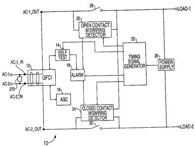
Fig. 1 is a functional block diagram of a preferred embodiment of the present
invention;
Fig. 2 is a detailed schematic diagram of a power supply circuit which may be
utilized within the embodiment of Fig. l;
8
~I'~~~1
Fig. 3 is a detailed schematic diagram of an audible alarm circuit which may
be utilized within the embodiment of Fig. 1;
Fig. 4 is a detailed schematic diagram of a timing signal generator which may
be utilized within the embodiment of Fig. l;
Fig. 5 is a detailed schematic diagram of an open-contact miswiring detector
which may be utilized within the embodiment of Fig. 1;
Fig. 6 is a detailed schematic diagram of a closed-contact miswiring detector
which may be utilized within the embodiment of Fig. 1;
Fig. 7 is a detailed schematic diagram of the ground fault circuit interrupter
which may be utilized within the embodiment of Fig. 1;
Fig. 8 is a detailed schematic diagram of an automatic gain control circuit
which may be utilized within the embodiment of Fig. l;
Fig. 9A is a detailed schematic diagram of a portion of self test circuitry
which
may be utilized within the embodiment of Fig. l; and
Fig. 9B is a detailed schematic diagram of a portion of the self test
circuitry
which may be utilized within the embodiment of Fig. 1;
DETAILED DESCRIPTION OF THE INVENTION
A preferred embodiment of an Intelligent Ground Fault Circuit Interrupter
(IGFCI) System 10 (hereinafter referred to interchangeably as "IGFCI",
"system"
and "device") of the present invention will now be described in accordance
with Fig.
1. The IGFCI 10 shown therein preferably includes a standard Ground Fault
Circuit
Interrupter (GFCI) 12 as its "core" structure, readily known to those skilled
in the art,
a self test circuit 14, open-contact and closed-contact miswiring detectors
20, 24, an
alarm circuit 18 and an automatic gain control circuit 16. Installed properly,
the
system 10 protects all downstream electrical devices connected to it as well
as any
receptacles present in the device itself. It should be noted, however, that
the
9
description of the preferred embodiment is presented merely for illustration
purposes
only and is not meant to limit the scope or spirit of this invention.
Fig. 1 shows the IGFCI 10 as a four terminal device which includes power
input terminals AC-l and AC-2, referred to hereinafter as phase and neutral
line
terminals, and system output terminals LOAD-1 and LOAD-2, referred to
hereinafter
as phase and neutral load terminals. An AC power source (not shown in the
figure) is
connectable to the device 10 to provide AC power therein via phase and neutral
line
terminals AC-1 and AC-2. A metal oxide varistor (MOV) 270 is shown
electrically
connected between phase and neutral line terminals for suppressing voltage
spikes.
The GFCI 12 is disposed in a current path for alternating current flow from
the AC
source to the load. The GFCI includes line (AC-1 IN, AC-2 IN) and load side
(AC-
1 OUT, AC-2 OUT) phase and neutral ports, wherein AC-1 IN and AC-2 IN
electrically connect the GFCI to phase and neutral line terminals of the AC
source.
The GFCI is also electrically connected to a self test circuit 14, a first
contact 28 of a
relay switch 31 at terminal AC-1 OUT and to a second relay contact 30 of
switch 31
at neutral line terminal AC-2 OUT.
Also connected to the line side of relay contact 28 is a phase port of the
open-
contact miswiring detector (OCMD) 20, a load port of which is electrically
connected to the load side of relay contact 28, phase load terminal LOAD-1 of
the
IGFCI and a phase port of the CCMD. The closed-contact miswiring detector
(CCMD) 24 is electrically connected at a line side phase port to both GFCI
load side
neutral .terminal AC-2 IN and to a line side of relay contact 30, and at a
load side
neutral port to both a load side of relay contact 30 and IGFCI load side
neutral
terminal LOAD-2.
The IGFCI 10 also includes a power supply 26 which provides DC for the
IGFCI from the AC source. A phase port of power supply 26 is electrically
connected to phase load terminal LOAD-1 and the load side of relay contact 28.
A
~1'~:~~.~~
neutral port of the power supply is electrically connected to neutral load
terminal
LOAD-2, and the load side of relay contact 30. The power supply generates and
supplies DC to the system (i.e., Vcc and Vcc/2, which are not shown in the
system
diagram of Fig. 1). A frequency calibration signal port is electrically
connected to an
input port of a timing signal generator 22. Timing signal generator 22 is
electrically
connected to timing ports of open and closed miswiring contact detectors 20,
24, to
self test circuit 14 and to alarm circuit 18, respectively. Alarm circuit 18
is also
electrically connected to self test circuit 14, open-contact miswiring
detector 20 and
closed-contact miswiring detector 24.
One of the key features of the IGFCI 10 is the device's ability to detect
improper installation, i.e., miswiring, to an electrical wiring system in
which it is
installed. The most common cause of miswiring occurs when the AC power source
is connected to the LOAD-1, LOAD-2 terminals and the load is connected to the
AC-
1, AC-2 terminals. The present invention anticipates such miswirings whether
the
contacts are open or closed. More particularly, the open-contact miswiring
detector
20 detects a miswiring condition when relay contacts 28, 30 are in an open
state, and
the closed-contact miswiring detector 24 detects miswiring when the relay
contacts
are in a closed state.
Relay contacts 28, 30 pass AC to the load if the GFCI 12 maintains the
contacts in a closed state. Automatic Gain Control circuit (AGC) 16
continually
adjusts the sensitivity of the GFCI to track or compensate for ground leakage
current
typically generated by loads attached to the system, i.e., appliances such as
refrigerators, dishwashers, washing machines, etc. The ground leakage current
in
many such appliances can cause nuisance tripping of GFCIs if the appliances
are
located on a shared branch circuit, such as the GFCI, due to the design of
electrical
circuitry contained therein. Accordingly, the IGFCI, through the automatic
gain
control current, recognizes and adjusts for this type of leakage current. The
self test
11
circuit 14 interfaces with portions of the GFCI core circuitry to provide for
unaided,
unattended self testing of the entire GFCI circuit including its SCR and trip
coil.
Power supply 26 generates the DC electrical voltages needed by the internal
circuitry of the device 10 via DC connections identified in Figs. 2-8, 9A and
9B, and
includes phase, neutral and frequency calibration (i.e., 60 HZ, to be
discussed in
greater detail below) ports. The device 10 utilizes voltages of 12 and 6
volts, i.e.,
Vcc and 1/2Vcc, respectively. Timing signal generator 22 generates the signals
which ultimately alert the user of a need to test the device 10, as well as
triggering
periodic internal self tests. The alarm circuit 18 is meant to indicate an
alarm state to
a user, for example, an audible signal to communicate various alerts to a user
such as
when a miswiring situation exists. In the preferred embodiment, the alarm
circuit
includes a ceramic piezo element as the sound producing component that
actually
generates the alarm sound. As an alternative, sound may be produced by a
speaker,
buzzer or other sound generating element known to those skilled in the art.
Alternatively, it is envisioned that the alarm circuit generates a flag signal
which may
be transmitted to a sensor linked to a digital computer, which acts
accordingly.
The circuits which define the embodiment of the present invention shown in
Fig. 1 and briefly described above will now be explained in greater detail
with
reference to Figs. 2-8, 9A and 9B. In the figures, like numerals will define
like
terms.
Fig. 2 is a detailed schematic diagram of one embodiment of power supply 26,
previously identified in Fig. 1. Power supply 26 is shown electrically
connected at its
phase port to the load side of relay contact 28 and terminal LOAD-1; the
frequency
calibration port outputs a zero crossing, or clock, signal "60HZ" which is
generated
therein to synchronize system or device 10 operation. The power supply
rectifies
AC supplied through the GFCI 12 across contact 28 while operational, thereby
providing a 1/2Vcc signal and a Vcc signal to the rest of the system.. The
power
12
w. F
supply is preferably a CMOS device in order to minimize total power
dissipation for
the device 10 averages between 10 to 20 milliwatts.
A preferred form of the power supply circuit is as follows. A resistor 32,
having a nominal value of between 10 and 20 ohms, is electrically connected at
a first
end to the load end side of relay contact 28 and at a second end to both a
first end of a
capacitor 36 and a first end of a resistor 34. Second ends of resistor 34 and
capacitor
36 are electrically connected to the timing signal generator 22, as mentioned
above,
to a cathode end of a zener diode 38 and to an anode end of a diode 40.
Capacitor 36
serves as a series impedance to reduce the AC line voltage at the load end
side of
contact 28 when the power requirement on the supply is relatively low;
capacitor 36
also aids in power factor correction. By defining capacitor 36 with a 1 ~F
value, an
equivalent impedance of approximately 2.6 KS2 is generated at 60 Hz. Resistor
34, in
parallel with capacitor 36, is designed with a high value (around 100 K ohms)
to limit
the current through the zener diode 38. Zener diode 38 displays a breakdown
value
of approximately 15 V in order to pre-regulate the incoming AC voltage. The
zener
diode 38 also defines the origin of the zero crossing signal, 60HZ, the clock
input to
timing signal generator 22.
Cathode end of diode 40 is electrically connected to an anode end of a storage
capacitor 42, a first end of a current-limiting resistor 44, and collectors of
NPN
transistors 50, 48, 58. Diode 40 provides half wave rectification for storage
capacitor
42, which supplies current to zener diode 46 and prevents the discharge of
storage
capacitor 42 during the negative half cycle of the AC source. A second end of
resistor 44 is electrically connected to both a base of transistor 48 and a
cathode end
of a second zener diode 46. Resistor 44 supplies current from storage
capacitor 42
for zener diode 46, which displays a breakdown voltage of 13 V to maintain a
constant voltage at NPN transistors 48, 50. Anode ends of zener diodes 38, 46
and
cathode end of storage capacitor 42 are electrically connected to ground.
13
An emitter of transistor 48 is connected to a base of transistor 50, and an
emitter of transistor 50 is connected to a collector of an NPN transistor 60
(defining
Vcc). An emitter of transistor 58 is electrically connected to a base of
transistor 60,
an emitter of which provides '/Z Vcc. A collector of transistor 60 is
electrically
connected to a first end of a resistor 54, a first end of a storage capacitor
56 and a
base of transistor 58. Cathode end of storage capacitor 56 and second end of
resistor
54 are electrically connected to ground. Storage capacitor 56 helps to
maintain the
base of transistor 59 at a constant voltage in the event transients appear on
Vcc.
Resistors 52, 54, are defined to be approximately 100 KS2 to form a voltage
divider
whose output is approximately one half the Vcc voltage for regulating the NPN
transistor pair 58, 60. Consequently, a constant voltage of approximately'/2
Vcc is
supplied from the emitter of transistor 60. The reduced '/2 Vcc voltage serves
as a
reference voltage for some of the voltage comparators used in the circuitry of
device
10. Because power supply 26 is connected to the AC source on the load side of
relay
28, no power is provided to the system the relays 28, 30 trip for any reason.
Fig. 3 is a detailed schematic diagram of one embodiment of an alarm circuit
18, previously identified in Fig. 1. The alarm circuit 18 receives several
inputs from
circuits which have yet to be described in detail, for example, a MISWIRE_OPEN
bar signal is supplied from open-contact miswiring detector 20 (Fig. S), a
MISWIRE_CLOSED bar signal from closed-contact miswiring detector 24 (Fig. 6),
and a pair of SCR FAIL bar and GFCI FAIL bar signals from self test circuit 14
(Figs. 9A, 9B), all of which are supplied to a Nand circuit 62. The 'bar'
designation
after any signal name signifies that the signal is active low. The logical
output of
Nand circuit 62 provides an ALARM_TRIP signal to cathode ends of diodes 64 and
66. An anode end of diode 64 is electrically connected to a first end of a
resistor 65
to generate an input signal to a Nand circuit 70. Vcc is also connected to the
second
end of resistor 65 and logical Nand circuit 70. The logical output of Nand
circuit 70
14
~1'~~v~~~
is provided to a cathode end of a diode 80, an anode end of diode 66, and to
first ends
of resistors 72 and 76. Second end of resistor 76 is electrically connected to
a
cathode end of diode 74, the anode end of which is electrically connected to a
first
end of a discharge capacitor 78, a second end of resistor 72 and a second
input to
Nand circuit 70.
An anode end of diode 80 is electrically connected to Vcc through a resistor
82 and to an input of a logical Or circuit 84. A second input to Or circuit 84
receives
a TEST REMINDER signal from the timing signal generator 22 (to be described
below with reference to Fig. 4); the Or circuit logical output is electrically
connected
to a logical Nand circuit 86. A second input to Nand circuit 86 is
electrically
connected to the circuit's logical output through a resistor 88. The magnitude
of the
output (feedback) signal is held on a first end of a capacitor 90, the second
end of
which is grounded. The logical output of Nand circuit 86 is also electrically
connected to an input to PIEZO element 92, an output of which is connected to
ground, to generate an alarm. The PIEZO element is just one example of alarm
or
sound generation circuitry 18 which may be utilized in the system to produce
various
duration beeping or alarm sounds to communicate when the system 10 is in
certain
states, or at the occurrence of various events. For example, the alarm or
beeping
would signal a user in the event a miswiring condition were detected.
The actual frequency of the sound emitted by the circuit 18 is determined by
the values of resistor 88 and capacitor 90, which are coupled to gate 86 in a
classic
oscillator configuration. The charge and discharge of capacitor 90 causes the
Nand
circuit 86 logical output to swing back and forth or oscillate with a duty
cycle of
approximately 50% because capacitor 90 is charged and discharged through the
same
resistor 88. If, however, the output of Or circuit 84 goes low, oscillations
cease
because the output of Nand circuit 86 remains high no matter what appears
across
capacitor 90. Preferably, resistor 88 and capacitor 90 define an RC time
constant
1 ~ e.~ J ~ ~
which rings sound producing component 92 at between 2.5 to 3.0 KHz. As long as
the output of OR gate (circuit) 84 is high, the oscillator causes the
resonator 92 to
generate a tone.
Nand circuit 70, resistors 72, 76, diode 74 and capacitor 78 determine the
duty
cycle (i.e., the turn on and turn off times) of the oscillator built around
Nand circuit
86 to drive PIEZO element 92. The duty cycle of the tone, however, is not
symmetrical because resistors 72, 76 have different values, the parallel
combination
of which determines the off duration of the tone. Due to the blocking effect
of diode
74, resistor 72 alone determines the on duration of the tone. Resistors 72, 76
are
preferably chosen to produce an approximately 150 millisecond tone-on and one
second tone-off periods. Tone is produced when the ALARM TRIP signal is high
(i.e., diodes 64, 66 are reverse biased). This allows the output of logical
Nand circuit
70 to oscillate due to the charge and discharge of capacitor 78, similar to
the action of
capacitor 90 as discussed above.
The alarm signals input at logical Nand circuit 62 are generated by the system
when either a miswiring condition or a GFCI related failure is detected. A
low,
therefore, at any of these inputs causes the alarm circuitry 18 to output an
audio or
visual alarm to alert a user that a miswiring condition or failure has
occurred.
Conversely, keeping the tone or alarm indicia off, the non-feedback inputs to
logical
Nand circuits 70, 86 are held in the low state by the ALARM-TRIP signal,
causing
the logical signals output therefrom to remain in the high state which
prevents
oscillation. A low output from Nand circuit 62 is provided through diodes 64,
66
compelling the outputs of Nand circuits 70, 86 to remain in the high state.
Logical
Nor circuit 84 enables the oscillator driving the PIEZO element 92 with the
TEST REMINDER signal generated within the timing signal generator 22. This
TEST REMINDER signal functions to remind a user to periodically manually test
16
the device 10. When the TEST REMINDER signal is high, the resonator 92 will
produce a short alarm tone (or short infrared of visible light output) once
per minute.
Fig. 4 is a detailed circuit diagram of one embodiment of a timing signal
generator 22 described above in relation to Fig: 1. The combination timing
signal
generator and alarm circuit 18 contained within the present invention was
developed
in part because it was found that user instructions (accompanying conventional
GFCIs) for periodically testing the system or device at least once per month
are
typically ignored by the user. Further, most users are found to ignore the
clear
notices placed not only within the unit's installation instructions but even
those on
the face of the device itself. The timing signal generator attempts to
compensate for
this reality by causing to be generated a short chirping sound once every
minute to
remind a user to test the device once a test reminder signal is enabled
(preferably
every 30 days).
The timing signal generator 22 also generates test pulses used by built in
test
circuitry (self test circuit 14 identified as Figs 9A, 9B, to be discussed in
detail
below) to precipitate automatic self testing once every hour, and the power on
reset
signal (PWR ON RESET) which is used by the system 10 to put various
components in a known state when system power is initialized. At the. core of
the
signal generator 22 is a timer circuit 114, which may embody any monolithic
integrated circuit, group of MSI or LSI logic functions, ROM based sequencer
or
other clock driven circuit known to those skilled in the art that is capable
of counting.
Upon application of system power, the timer 114 generates PWR ON RESET and
PWR ON RESET bar signals, which are active immediately after power is applied
and are active for at least 100 msec. The 60HZ signal provided by the power
supply
26 (zero crossing signal generated across the zener diode 38) drives the
timer. All the
signals generated by the timer 114 are derived ultimately from this clock
input.
17
~1'~~~~
As mentioned above, 30 days after AC power is initially applied, the IGFCI
device 10 emits an active high test reminder signal, TEST REMINDER, to alert a
user of a need to manually test the device 10. To do so, the user presses a
momentary
switch button 94 (not shown in Fig. l ) located on the face of the device 10,
one end of
which is connected to the LOAD-1 terminal. An opposite end of switch 94 is
electrically connected to a first end of a resistor 96, a second end of which
is
connected to terminal AC-2. The first end of resistor 96 is also electrically
connected
to a first end of a resistor 98, a second end of which is connected to an
anode end of a
diode 100. A cathode end of diode 100 is electrically connected to a first end
of a
resistor 102, an anode end of a diode 106, a reset input to timer 114, and a
first end of
a resistor 112. A second end of resistor 112 is electrically connected to a
first end of
a capacitor 113, a second end of which is connected to ground, and also as a
GND
input to timer 114. Cathode end of diode 106 is electrically connected to Vcc
and an
anode end of a diode 108. A cathode end of diode 108 is electrically connected
to a
first end of a capacitor 110, a second end of which is connected to ground,
and as a
Vdd input to timer 114.
In addition to the POWER ON RESET, POWER ON RESET bar signals
mentioned above, the timer also generates 1 SOMS, 300MS, 1 MIN, 1 HR, 2HR,
60 DAY, 120 DAY and 240 DAY signals. Signals 60 DAY, 120 DAY and
240 DAY are provided as inputs to a logical Or circuit 146, an output of which
is
provided to a logical Nand circuit 126 along with the 1MIN and DAY signals
generated by a DAY signal generator circuit 117. Within the DAY signal
generator
circuit 117, a first end of a resistor 120 is electrically connected to an
anode end of a
diode 124. Second end of resistor 120 is electrically connected to first ends
of a
resistor 116, and a photoresistor 118, which are electrically connected in
parallel to
Vcc. Second ends of resistors 116 and 118 are electrically connected to a base
and
emitter of an NPN transistor 119, respectively. An emitter transistor 119 is
18
~1'~ i~~~~
electrically connected to a first end of a resistor 122, a second end of which
is
grounded, and to a cathode end of a diode 124.
The PWR ON RESET bar is provided to each of three logical Or circuits
128, 130 and 132. 150MS is provided to logical Or circuits 130 and 132, and
300MS
is provided to logical Or circuit 128. The output of logical Or circuit 128 is
provided
as an active-low reset to a D-type latch circuit 134. An output from logical
Nand
circuit 126 is provided as a clock input to the latch circuit; Vcc holds the
circuit's
"D" input high through a resistor 140. Also included are "D" type latch
circuits 136
and 137, which are electrically connected via pull-up resistors 142 and 144 to
Vcc.
The 1HR and 2HR signals are electrically connected as clock inputs to the f/f
circuits
136 and 138, respectively from the timer 114. Signals output from logical Or
circuits
130 and 132 are electrically connected to the f/f circuits 136, 138 as active
low reset
inputs. Finally, TEST REMINDER, 1HR PULSE bar and 2HR PULSE bar signals
are the logical outputs emanating from the "Q", "Q bar" and "Q bar" outputs of
latch
circuits 134, 136 and 138, respectively
Actuation of momentary switch 94 simulates a ground fault by momentarily
causing the current flowing into the device via terminals AC-1 and AC-2 to
differ. If
working properly, the GFCI circuit 12 (Fig. 7) detects the current-flow
difference via
magnetic cores 312, 314, and generates an SCR control signal thereby. As a
result,
the SCR 244 within the GFCI is triggered, the relay trip coil 260 is energized
and the
relay contacts 28, 30 of the IGFCI are exercised. Pressing the test button 94
also
causes the timer 114 to reset by resetting its internal counters and beginning
again a
count of a 30 day period.. The timer's reset input, which is active high, is
coupled to
the TEST BUTTON signal through resistor 98 and diode 100. Resistor 102 and
capacitor 104 provide filtering for the reset input signal.
The "D" latch circuit 134, therefore, operates as a one-shot and generates a
1 SO ms long high pulse once every minute, i.e., the TEST REMINDER signal.
Since
19
l x~~t'~
its input is pulled high through resistor 140 to Vcc on each rising edge of
its clock
input, a logical high is clocked in to the latch circuit and appears at the
circuit's "Q"
output. The output of logical Nand circuit 126 goes high when all its inputs
are high.
Approximately 30 days after power is initially applied to the device 10, the
60 DAY
signal goes high causing the output of logical OR circuit 146 to go high. If
the DAY
signal and the 1MIN signals also go high, latch ("D" f/f) circuit 134 gets
clocked and
a logical high appears at the circuit's "Q" output. Approximately 150 ms
later, the
300MS signal from timer 114 goes low and resets the latch circuit 134 "Q"
output to
a logical low. The 300MS signal is gated with the PWR ON RESET bar signal to
allow either signal to reset the latch circuit 134. This reset signal can also
reset latch
circuits 136, 138 through logical Or circuits 130, 132 respectively.
The DAY signal output from circuit 117 is driven high when the intensity of
the light surrounding the IGFCI device 10 sufficiently lowers the resistance
of
photoresistor 118. Consequently, increased current flows through the emitter
of
transistor 119 and resistor 122, reverse biasing diode 124 and the voltage
level of the
DAY signal to be pulled up to Vcc. When there is insufficient light intensity
(i.e., at
night), the resistance of photoresistor 118 is very high which limits current
flow
through resistor 122 to reverse bias diode 124. Resistor 122 then sinks
current to
ground keeping the output of Nand circuit 126 a logical low. This prevents the
TEST REMINDER signal from sounding during the evening and night hours, the
time most people are asleep. If the user fails to heed the once a minute
TEST REMINDER signal, commenced after 30 days, the signal will remain active
for approximately another 210 days after which the timer 114 resets itself. If
at any
time during the 210 days the user manually tests the device 10, the timer 114
resets
and begins again counting the 30 day period again. The 120 DAY, 240 DAY clock
signals are ORed with the 60 DAY in logical Or circuit 146 to form one of the
three
inputs to logical Or circuit 126, each of which may cause a change of state in
the
latch circuit 134 output, i.e., the TEST REMINDER signal.
Another key feature of the IGFCI system 10 is its ability to detect a
miswiring
condition when the system is wired with the contacts of contact relays 28, 30
in either
an open or closed state. This is very important because it is impossible to
predict
what state the relay contacts will be in when AC power is first applied. Open-
contact
miswiring detector 20 detects and memorizes, using latch circuit 174, whether
the AC
power is wired correctly to the AC-1, AC-2 terminals, or incorrectly to the
LOAD-1,
LOAD-2 terminals. This detection takes place at a point in time shortly after
power
is initially applied. If the device 10 is installed with the relay switches
28, 30 already
in the closed position, which is a real possibility, the detection circuitry
20 defaults,
in which case a determination of proper or improper wiring must be made by the
closed-contact miswiring detector 24.
A detailed circuit diagram a preferred form of an open-contact miswiring
detector 20 will now be described with reference to Fig. 5. AC-1 IN terminal
is
shown in the figure electrically connected to an anode end of diode 148 and
line side
end of contact 28; the load side end of contact 28 is electrically connected
to both the
LOAD 1 terminal and an anode end of a diode 160. Cathode ends of diodes 148,
160 are electrically connected to first ends of resistors 150, and 162,
respectively.
Second ends of resistors 1 SO and 162 are connected to first ends of resistors
152, 164,
respectively, and also to a base of NPN transistors 156 and 168, respectively.
Emitters of transistors 156, 162 are grounded and collectors are connected
through
resistors 154, 156, respectively, to Vcc. A second end of resistor 152 is
connected to
terminal AC-2 OUT, the line side end of contact 30, a first end of a resistor
1 S 1 and
a first end of a capacitor 153. Accordingly, resistor combination 1 S0, 152
acts as a
voltage divider to bias the base of transistor 156.
21
~1'~~~~~.
The collector of transistor 156 also is electrically connected to both a
logical
Or circuit 175 and a logical And circuit 172. A second end of resistor 164 is
electrically connected to load side end of relay contact 30, a second end of
resistor
151 and a second end of capacitor 153. Resistor combination 162, 164 together
form
a voltage divider which defines the base input to transistor 168. The
collector of
transistor 168 also is electrically connected to Or circuit 175 and as dual
inputs to a
logical Nand circuit 170. An output of Nand circuit 170 is provided as a
logical input
to And circuit 172. An output of And circuit 172 is provided as a "D" input to
a latch
circuit 174.
The functioning of detector circuit 20 is dependent upon NPN transistors 156,
168, which are arranged to detect AC power between the AC line side and LOAD
terminals. If an AC power source is correctly wired to the terminals AC-1, AC-
2,
and, if the contacts of relays 28, 30 are in the open position, AC power is
applied
only across diode 148. The LOAD side of the relays 28, 30 are left without AC
power. Collector current flows through resistor 154 from Vcc to ground and a
logic
low is applied to the input of logical And circuit 172. Accordingly, the input
to latch
circuit 174 is a logical low regardless of the state of transistor 168 as long
as AC
power is applied across terminals AC-1, AC-2. Timing signal generator 22 (Fig.
4)
supplies the PWR ON RESET bar signal as a clock input to latch circuit 174,
the
leading edge of which clocks the "low" input out as a "Q bar" signal defining
a
MISWIRE_OPEN bar signal in a high state (i.e., no miswiring condition).
Therefore,
if power is applied with the contacts 28, 30 open, the output signal from the
detection
circuitry 20 remains high.
Alternatively, if AC power is wired incorrectly to the LOAD-1, LOAD-2
terminals, and the relay contacts 28, 30 are in the open position, transistor
156
remains off and resistor 154 pulls one input to And circuit 72 logically high
upon the
application of AC power. Current therefore flows through diode 160 and is
divided
22
~ ~.'~ ~. ~ 1
within a voltage divider formed by resistors 162, 164, turning on transistor
168. In
consequence, current flows through resistor 166, grounding the inputs to
logical Or
circuit 170. The Or circuit logical output goes high which causes the signal
output
from latch circuit 174, MISWIRE OPEN, to go low upon the rising edge of the
PWR ON RESET bar signal. A low MISWIRE_OPEN bar signal triggers the alarm
circuitry 18 which alerts the user that a miswiring condition exists. Since
timer 114
of timing signal generator 22 is synchronized to the 60HZ signal, the rising
edge of
the PWR ON RESET bar signal does not occur at a zero crossing but at a point
within the AC cycle at which the data operating as logical inputs to Nand and
And
circuits 170, 172, are reliable.
If AC power is incorrectly wired to the LOAD-1, LOAD-2 terminals, and
relay contacts 28, 30 are closed, application of AC power will prevent the
open-
contact miswiring detector 20 from triggering the alarm. The MISWIRE_OPEN bar
output signal therefore remains high. Consequently, deference is made to
closed-
contact miswiring detector 24 for determining whether the device 10 is wired
correctly and logical Or circuit 175 generates a CONTACT CLOSED bar signal
from the collector outputs of transistors 156, 168, which are low only when
relay
contacts 28, 30 are in the closed state. Closed-contact miswiring detector 24
utilizes
the CONTACT_CLOSED bar signal to determine whether the GFCI circuitry 12 is
properly wired. If the relay contacts 28, 30 are open, control passes from the
closed-
contact miswiring detector 24 to the open-contact miswiring detector 20 for
the
determination whether the device 10 is wired properly.
Referring now to Fig. 6, a preferred form of the closed-contact miswiring
detector 24 described above with reference to Fig. 1 will be described.
Because
mechanical relay contacts 28, 30 exhibit a finite ohmic resistance, a
detectable
voltage drop is generated across each at power up when the contacts are in
their
closed state. More particularly, upon system power-up, the system 10 simulates
a
23
2I~~LW'
load which draws 2 to 3 amps on the load end sides of contacts 28, 30 for a
time
period of approximately 250 .sec. This burst of current generates a finite
voltage
drop across the equivalent impedance of the relay contacts 28, 30, which is on
the
order of 3 mS2. This voltage drop can be detected and amplified using standard
components and will only be generated if the device 10 is wired correctly. If
it is
improperly wired, no voltage drop will appear across the relay contacts. In
the
preferred embodiment, the voltage drop across only one of the relay contacts,
relay
contact 28, is detected. However, either relay contact 28, 30 could be used to
detect
the presence of the voltage developed across its equivalent "on" impedance.
Line side end of contact 28 is electrically connected to terminal AC-1 OUT of
GFCI 12 and first ends of resistors 182, 184, and a capacitor 186. A second
end of
resistors 182, 184 and a first end of capacitor 188 are electrically connected
to the
load end side of relay contact 28 and to terminal LOAD-1. Second end of
capacitors
186, 188 are electrically connected, respectively, to inverting and non-
inverting
inputs of op-amp 190. The inverting input to op-amp 190 is also electrically
connected to a cathode end of a diode 189, an anode end of a diode 187 and a
first
end of a resistor 181. The non-inverting input to op-amp 190 also is
electrically
connected to an anode end of diode 189, a cathode end of diode 187 and a first
end of
a resistor 183. Second ends of resistors 181, 183 are connected respectively
to a first
end of resistor 178 and a second end of resistor 176, and, a second end of
resistor 178
and a first end of resistor 180. First end of resistor 176 is connected to Vcc
and
second end of resistor 180 is grounded. An output of op-amp 190, a CONTACT-
CURRENT signal, is electrically connected a logical Or circuit 207.
Also electrically connected to terminal LOAD-1 is an anode end of a diode
202; a cathode end of diode 202 is electrically connected to first ends of
resistors 204
and 192. Second ends of resistors 204 and 192 are each electrically connected
to a
drain of FET 206 and an anode end of diode 196. A cathode end of diode 194 is
24
electrically connected to both a first end of a resistor 196, a second end of
which is
connected to terminal LOAD-2, and a base of an NPN transistor 200. An emitter
of
transistor 200 also connects to terminal LOAD-2, while its collector
(CURRENT FLOW signal) electrically connects to a gate of FET 206, a first end
of
a resistor 198, and an input to a Nand circuit 208. The PWR ON RESET signal,
generated by timer 114 within timing signal generator 22 is provided to a
second end
of resistor 198 to control the state of the gate of FET 206.
The CONTACT CLOSED bar signal, generated within the open-contact
miswiring detector 20 is input to Or circuit 207 with the CONTACT CURRENT
signal. An output of Or circuit 207 is provided as a "D" input to a latch
circuit 212.
The CURRENT FLOW signal is provided into Nand circuit 208, an output of which
(CURRENT FLOW bar), with the PWR ON RESET bar signal, are provided as a
clock input to the latch circuit 212 via logical Or circuit 210. A "Q" latch
circuit
output defines a MISWIRE-CLOSED bar signal. Upon device power-up, a positive
going PWR ON RESET pulse is provided by timer 114 as an Or circuit 210 input,
to
the collector of transistor 200 and to the gate of n-channel MOSFET 206
through
resistor 198 (100 Kohms). The PWR ON RESET signal has a minimum duration of
at least one complete AC cycle. The time length of the pulse is defined to
overlap at
least one negative-to-positive-going zero crossing of a power signal generated
by the
AC power source. MOSFET 206 is used as a voltage controlled switch to control
the
flow of current from the AC power source through resistor 204. Having a value
of
approximately 1-2 ohms, resistor 204 allows approximately 2-3 amps to flow
through
the relay contacts 28, 30 when the AC line voltage reaches approximately 4-5
volts.
Current flow through resistor 204 is restricted to the positive half cycle due
to
the blocking effect of diode 202. In addition, MOSFET 206 can only turn on at
a
negative to positive zero crossing due to the action of transistor 200.
Resistors 192,
196 and diodes 202, 194 provide base current during the positive half cycle to
effectively clamp the gate of MOSFET 206 to ground, preventing it from turning
on.
However, sufficient base current is not generated until the AC line voltage
reaches
approximately 4-5 volts. Thus, current is allowed to flow through resistor 204
until
the AC line voltage reaches 4-5 volts, whereupon transistor 200 turns on,
grounding
the gate of MOSFET 206, effectively turning it off. Current flow through
resistor
204 produces a voltage drop of approximately 10 rnV across relay contacts 28,
30, for
approximately 250 .sec. The gate of MOSFET 206 is the source for the
CURRENT FLOW signal which is inverted before being ORed with the
PWR ON RESET bar signal by Or circuit 210.
If the device is properly wired to the AC power source while the contacts are
closed, voltage comparator 190 detects and amplifies the voltage drop produced
across the equivalent ohmic resistance 182 of the relay contact 28. Both sides
of
relay contact 28 are coupled to the inputs of voltage comparator 190 through
0.01 ~F
capacitors 186, 188. These capacitors provide isolation between the
comparator's
190 reference voltage and circuit ground. The voltage divider, consisting of
resistors
176 ( 10 MSZ), 178 ( 1 KS2), 180 (2 MS2), supplies the reference voltage
needed by
comparator 190 to determine whether the IGFCI device 10 is correctly wired.
Resistors 181, 183 protect the inputs of the comparator 190 when the relay
contacts
28, 30 are in the "open" position by limiting the current between the AC power
source side and the load side of the relay contacts 28, 30. Back to back
diodes 187,
189 limit the voltage potential between the amplifier inputs to a diode drop
to protect
it against damage due to excessive voltage.
If the device is correctly wired, a positive pulse signal (i.e., a 12 volt
signal) appears at the output of comparator 190. This active logical high
signal,
CONTACT CURRENT, is clocked into latch circuit 212 after first being gated
with
the CONTACT CLOSED bar signal in Or circuit 207. The "Q" output is an active
26
low signal, MISWIRE CLOSED bar, and is only at a logical low when both relay
contacts 28, 30 are in the closed state, otherwise MISWIRE_CLOSED bar is high.
If MISWIRE_CLOSED bar is at a logical high, then the relay contacts 28, 30
are open and the latch circuit input is at a logical high no matter what the
logical level
of CONTACT CURRENT signal. This is to assure that the circuit 212 output
signal,
MISWIRE CLOSED bar, remains high in the event the relay contacts 28, 30 are in
the open state in accordance with open-contact miswiring detector 20 to
determine
whether a miswiring condition exists. The signal provided by Or circuit 210
remains
at a logical high level from the zero crossing until the AC reaches 4-5 volts.
At that
point, transistor 200 turns on and sinks the signal at the gate of MOSFET 206
to
ground, causing CURRENT FLOW to go low. This signal is inverted by Nand
circuit 208, the rising edge of what is used to clock the level of
CONTACT CURRENT to the output of latch circuit 212. The output,
MISWIRE-CLOSED bar, is high if no miswiring condition is sensed, and low, if a
miswiring condition is sensed.
If the device 10 were incorrectly wired (i.e., the AC power source was
connected to the LOAD-l, LOAD-2 terminals), and the relay contacts 28, 30 are
closed, the current produced by resistor 204 would not flow through the
contacts 28,
30. This is because the current path extends from the LOAD-1 terminal through
diode 202, resistor 204, MOSFET 206 to the LOAD-2 terminal. Consequently, no
current flows through relay contacts 28, 30, which causes the output of
comparator
190 to go low. The CONTACT CLOSED signal is therefor driven low, since AC
appears on both sides of the relay contacts 28, 30. Correspondingly, when
latch
circuit 212 is clocked, MISWIRE_CLOSED bar goes low, triggering the alarm,
alerting the user that the device 10 is incorrectly wired and causing the
relay contacts
28, 30 to be tripped by the optocoupler 248 (Fig. 7).
27
A preferred embodiment of a GFCI circuit 12, described broadly above in
relation to Fig. 1, will now be described with reference to Fig. 7. IGFCI
terminals
AC-1 and AC-2 are electrically connectable to phase and neutral lines of the
AC
source and to GFCI phase and neutral line terminals AC-1 IN and AC-2 IN. A
first
or phase conducting element 21 I connects terminal AC-1 IN to terminal AC-
1 OUT, and a second or neutral conducting element 213 electrically connects
terminal AC-2 IN to terminal AC-2 OUT. Terminals AC-1 OUT and AC-2 OUT
are also electrically connected to line sides of contacts 28, 30,
respectively.
Conducting elements 211 and 213 are positioned such that they extend through a
pair
of magnetic cores 312, 314 which sense AC flowing into and out of the IGFCI
device
10.
Terminal AC-I OUT also is electrically connected to a first end of relay coil
260; a second end of relay coil 260 is electrically connected to an anode end
of a
diode 252 and a cathode end of diode 256, which together with diodes 254, 258,
form
a portion of a diode bridge. Cathode ends of diodes 252, 254 are electrically
connected to an anode end of an SCR 244. The cathode end of SCR 244 is
connected
to a first end of a resistor 246, a second end of which is connected to
floating ground,
as well as to an emitter gate of a transistor 249 of an optoelectronic switch
248.
Anode end of SCR 244 also is electrically connected to a first end of a
resistor 242
and a collector of transistor 249 of switch 248.
Magnetic core 312 generates a signal AGC IN which is proportional to an
amount of current flowing into the GFCI and provides the signal as input to
pins 2
and 3 of the LM1851 228; the AGC IN signal is also provided to the automatic
gain
control (AGC) circuit 16 (Fig. 8). Magnetic core 314 generates a signal which
is
proportional to an amount of current flowing back from the GFCI (in the
neutral) and
provides the signal across a capacitor 226. A first end of capacitor 226 is
also
connected to a second end of a capacitor 222 as input to pin 4 of the LM1851
and to
28
~1'~~a~~~
anode ends of diodes 256, 258. A second end of capacitor 226 is electrically
connected to pin 5 of LM1851 228.
The LM1851 228 is an integrated circuit which, via its input pins, detects
small differences in the current flowing through the AC-1 and AC-2 terminals,
identifying ground faults thereby. Upon detection of a ground fault, the
LM1851 228
conveys the fault information via the state of a signal, GFCI OUT, provided at
pin 1.
Pin 1 is electrically connected to a first end of a resistor 230, a second end
of which is
connected to a first end of a capacitor 240 and a gate of an SCR 244. The
state of the
pin 1 output (i.e., signal GFCI OUT) controls the state of SCR 244 by
integrating
the GFCI output. In other words, a particular level at capacitor 240, referred
to as the
SCR GATE signal, controls the impedance state of the SCR. SCR GATE defines
the state of conduction within the SCR path to ground, which in turn defines
the
current flow from terminal AC-1 through conductive element 211, through the
relay
coil 260, diode 252, the conducting path of SCR 244, and resister 246; the
neutral
line current flows through diode 258, element 213 to AC-2. Current flow
through the
coil 260 forces the relay contacts 28, 30 to an open state, cutting off power
to the load
and preventing a user from being injured.
AGC circuit 16 (Fig. 8) is electrically connected to the GFCI 12 across first
and second ends of a resister 232, preferably having a value of around 2 MS2.
The
signal output from the AGC circuit across resistor 232, varies the sensitivity
of the
LM1851 228 to leakage current detected in the system. A first end of resistor
232
also is electrically connected to pins 8 and 6 of the LM1851, and the
resistor's second
end is connected to pin 8, a cathode end of a diode 234 and an anode end of a
storage
capacitor 236. Pin 7 of the LM1851 is electrically connected across a
capacitor 238
to floating ground.
As mentioned above, SCR GATE controls current flow through SCR 224, and
the collector and emitter of transistor 249 of optocoupler 248 is connected
across the
29
~l d~ ~v~~
anode and cathode ends of SCR 244. The optocoupler is responsive to an
ALARM TRIP signal, generated within the alarm circuitry 18, and provided at
photodiode 251 . When ALARM TRIP goes high, i.e., an alarm condition occurs,
current flows through the photodiode to ground through resistor 250. This
causes the
optocoupler to turn on creating an alternate path for current which bypasses
the SCR
and energizes the coil 260 thereby opening relay contacts 28, 30: Thus, the
optocoupler serves as a backup or alternate means of tripping the relay
contacts 28,
30, either when the SCR has failed or when a failure in the GFCI 12 circuitry
has
been detected.
Another key feature of the system 10 of this invention is its ability to
dynamically adjust the leakage-current sensitivity of the GFCI circuit 12
using
automatic gain control (AGC). Currently, certain appliances are not required
to be
protected by a GFCI because they generate undesirable parasitic ground leakage
current that would interfere with the normal operation of a GFCI. Appliances
such as
refrigerators, dishwashers, washing machines, etc. or devices with switching
power
supplies in them, for example, typically use capacitors in their filter
circuits. These
capacitors usually are connected directly to the ground wire of the AC power
line,
thus generating ground leakage and causing "nuisance tripping" of the GFCI.
Because the IGFCI of this invention overcomes the problems associated with
such
appliances, it is foreseen that IGFCIs will become a UL requirement within the
same.
A preferred embodiment of an automatic gain control (AGC) circuit 16,
described broadly above with reference to Fig. l, will now be described with
reference to Fig. 8. The AGC circuit 16 detects and compensates for slow
rising,
steady and fast rising leakage current. In other words, the AGC circuit
distinguishes
between fast rising leakage current caused by a human and steady or slowly
rising
leakage current caused by certain appliances or other devices. In a case where
the
leakage current steadily increases, the GFCI tracks this increase and raises
its internal
reference threshold level for tripping, above which an additional 5 ma will
trip the
GFCI. In a case of steady state or slowly rising leakage current, up to 25 ma
can be
compensated for by the AGC circuit 16. However, any leakage current above 30
ma
will trip the GFCI. Although the quiescent or steady state sensitivity can
increase,
the GFCI's dynamic sensitivity does not change. At all times, 5 ma of fast
rising
leakage (i.e., that produced by human contact) will trip the GFCI circuit 12.
In order to receive the AGC IN signal from the GFCI 12, first ends of
capacitors 340, 342 are coupled to GFCI core 312 . The capacitors prevent the
AGC
circuit 16 from interfering with current sensing by the GFCI 12. Second ends
of
capacitors 344 and 346 are electrically connected to first ends of resistors
344, 346,
the second ends of which are electrically connected to inverting and non-
inverting
inputs to op-amp 349, respectively. The second end of capacitor 342 also is
electrically connected through a resistor 348 to'/2 Vcc: An output of op-amp
349 is
electrically connected to cathode end of diode 350, an anode end of which is
connected to ground, and an anode end of diode 352.
Cathode end of diode 352 is electrically connected to a first end of a
capacitor
362, a first end of a resistor 358, a second end of which is connected to
ground, a first
end of a resistor 356 and a cathode end of diode 354. Anode end of diode 354
is
electrically connected to a first end of a capacitor 360, a second end of
which is
grounded, and to a first end of a resistor 368. A second end of capacitor 362
is
electrically connected to a base of NPN transistor 366 and to a first end of
resistor
364, a second end of which is connected to ground. An emitter of transistor
366 is
grounded while its collector is connected to a second end of resistor 368, a
first end
of resistor 280, a second end of which is grounded, and a base of transistor
286. An
emitter of transistor 286 is connected across a resistor 286 to ground and a
collector
is connected across a resistor 284 to a gate of FET 290. Second end of
resistor 284 is
also electrically connected to a first end of a transistor 282. A second end
of resistor
31
282 is electrically connected to a first end of a 500 Kohm resistor 292, a
second end
of which connects to a source of N-channel FET 292.
The signal output of amplifier 349 is rectified by diodes 350, 352, and
charges
capacitor 360 through resistor 356. The voltage that appears across the
capacitor 360
biases the base of transistor 286 through resistors 368, 280. Collector
current flowing
through transistor 286 causes the equivalent impedance of FET 290 to decrease.
The
FET1500Kohm resistor 292 series combination is electrically connected in
parallel
with the 2 MSZ threshold set resistor 232 (Fig. 7). Lowering the equivalent
impedance (2 MSZ) by a factor of 5 corresponds to lowering the sensitivity of
the
GFCI to 25 ma. As the impedance decreases, so does the sensitivity.
Consequently,
it takes more current to trip the GFCI 12, i.e., the steady state reference
threshold at
which the GFCI will trip. For example, a steady leakage current of 1 ma causes
the
impedance of the FET 290 to decrease so as to raise the leakage level at which
the
GFCI trips to 6 ma (i.e., 1 ma steady state threshold plus 5 ma fixed dynamic
threshold). A steady state leakage of 5 ma will set the FET 290 to an
equivalent
impedance of 1.5 MS2. The resulting impedance sets the sensitivity of the GFCI
to
ma (i.e., 5 ma steady state threshold plus fixed 5 ma dynamic threshold). The
maximum equivalent impedance of the FET 290 will raise the steady state
threshold
to 25 ma. Thus, any leakage over 30 ma will trip the GFCL
Similarly, a slowly decreasing leakage current changes the steady state
threshold, above which 5 ma will trip the GFCI. A decreasing leakage current
causes
the output of the amplifier 349 to decrease, reverse biasing diode 352. The
accumulated charge on capacitor 360 discharges through resistors 356, 358 to
ground
until it reaches the new level set by the output of amplifier 349. The drop in
voltage
across capacitor 360 causes a corresponding increase in the impedance of the
FET
290, the result of the decreased collector current flowing through transistor
286. This
causes a higher voltage to appear at the gate of FET 290. This higher gate
voltage
32
~1~~~~~
raises the equivalent impedance of the FET 290. The higher resistance combined
with set resistor 232, in parallel with the series combination of FET 290 and
resistor
292, lowers the GFCI circuit 12 threshold.
As discussed earlier, the dynamic threshold of the GFCI 12 never changes
from its preset level of 5 ma. Thus, if, for example, the steady state
threshold has
risen from 0 ma to 10 ma due to 10 ma of leakage current present on the AC
power
line, the device 10 would trip on S ma of fast rising leakage current, the
type caused
by humans. To accomplish this, the GFCI circuit 12 uses transistor 366 to
quickly
discharge capacitor 360 and the base of transistor 286. This causes the
equivalent
impedance of the FET 290 to revert back to its original 5 ma sensitivity
setting. Fast
rising leakage current of the type that could be caused by humans causes the
output
of amplifier 349 to rise quickly causing current to charge capacitor 362. The
voltage
across resistor 364 rises with rising capacitor voltage until sufficient to
turn on
transistor 366. Transistor 366 turning on quickly depletes the charge on the
base of
transistor 286, turning it off and also quickly discharges capacitor 360.
Another important feature of IGFCI device 10 is the device's ability to
constantly monitor the GFCI circuitry 12 to assure proper operation in its
task to
protect users against ground faults. To accomplish this task, a test circuit
14 is
included to perform a built in test to perform two independent self test
operations on
the GFCI ensure user safety. A first self test is performed once every hour
and
checks that the trip coil 260 and the SCR 244 are working properly. A second
test is
performed once every two hours and checks that the GFCI IC 228 is working
properly. First and second self test circuits will now be described with
reference to
Figs. 9A, 9B, respectively.
Referring now to Fig. 9A, a preferred embodiment of a first portion of self
test circuit 14 for implementation within the present invention will be
described. The
first self test portion is electrically connected to GFCI 12 within which the
coil 260
33
~1~~~~
and SCR 244 are tested in conjunction with the 1HR PULSE bar signal produced
by
the timing signal generator 22. Consequently, the SCR 244 is turned on by
SCR GATE near the end of the positive portion of the AC cycle, i.e., at
approximately 170 degrees. The presence of any current flowing through the SCR
244 is detected and identified by way of the SCR CURRENT signal. If no current
is
detected, the alarm is triggered and the relay switches 28, 30 are tripped by
the
alternate trigger means of optocoupler 248 (described above).
LOAD-1 terminal is electrically connected to a first end of a resistor 372 and
a
cathode end of a diode 370. Anode end of diode 370 is electrically connected
to
second end of resistor 372, an anode end of capacitor 374, a cathode end of a
zener
diode 376 and two inputs of a logical Nand circuit 378 as a 170 degree
sensitive
signal, 170 DEG. The 170 DEG signal is generated through the resister 372 and
capacitor 374 pair during the positive half cycle when capacitor 374 charges
through
resistor 372. The values are chosen so that the input to gate of circuit 378
rises high
enough to cause its output to go low at approximately 170 degrees into the
positive
half cycle, generating the 170 DEG bar signal. Zener diode 376 simply prevents
the
input voltage from rising high enough to damage the gate inputs of Nand
circuit 378.
The output of gate circuit 378 (170 DEG bar) is a normally high signal that
goes low
170 degrees into the positive half cycle of the AC and remains low up to the
zero
crossing.
The 1HR PILSE signal generated within timing signal generator 22 is
combined with the 170 DEG signal within a logical Nor circuit 380, an output
of
which is provided to a base of a transistor 384. A collector of transistor 384
is
connected through resistor 382 to Vcc and the transistor's emitter is
connected to
ground through a resistor 386. Thus, transistor 384 only turns on when both
inputs to
gate 380 are low. As mentioned earlier, the 1HR PULSE signal is approximately
75
ms long, straddling more than one cycle of the AC power. Current flowing
through
34
~~.~~a~~
transistor 384 produces a voltage across resistor 386, turning on the SCR for
approximately the final 10 degrees in the positive AC half cycle. During the
negative
half cycle, diode 370 quickly discharges capacitor 374 for the following
positive half
cycle.
If the trip coil 260 and the SCR 244 are functioning properly, current will
flow
through both of these components when transistor 384 turns on. It is at this
point that
the SCR CURRENT signal, shown in Fig. 7, will be at its maximum. This signal
is
provided to a pair of inputs to a logical Nand circuit 390, where it is
inverted to
generate SCR CURRENT bar, and to a cathode end of a zener diode 388.
SCR CURRENT bar presets a latch circuit 392 causing the latch circuit's "Q"
output
to immediately go high. 170 DEG bar and 1HR PULSE signals are input to logical
Or circuit 394, an output of which is provided to clock latch circuits 392,
396. A
"Q" output of latch circuit 392 is electrically connected as a D input to
latch circuit
396; PWR ON RESET bar is provided as its "preset" as well as to a "set" input
of
latch circuit 392. Consequently, the rising edge of the 170 DEG bar clocks the
logical output of latch circuit 392 into latch circuit 396. Previously, upon
power up,
latch circuit 392 is reset low and latch circuit 396 is reset high. If current
flows
through the SCR 244, then a high is clocked into latch circuit 396 and the
output,
SCR FAIL bar, remains high. The alarm, therefore, is not triggered. However,
if no
current is detected, then a low is clocked into latch circuit 396 and the SCR
FAIL bar
signal goes low, the alarm is triggered and the relays 28, 30 are tripped by
the
optocoupler 248. Since the input to latch circuit 392 is tied low, a low is
always
clocked from the latch circuit 392 Q output. Thus, in the absence of the
preset pulse
derived from SCR 244 current, latch circuit Q output defaults to a low,
indicating a
failure with the SCR 244 and/or the coil 260.
Referring now to Fig. 9B, a preferred embodiment of a second portion of self
test circuit 14 will be described. The 2HR PULSE signal generated within
timing
signal generator 22 is provided to the clock input to a latch circuit 410. The
clock
input is also electrically connected to a first end of resistors 398, 498. A
second end
of resistor 398 is electrically connected to a base of NPN transistor 400, an
emitter of
which is grounded and a collector of which provides a path out for the SCR
GATE
signal. A second end of resistor 408 is electrically connected to a gate of N-
channel
FET 406. A source of FET 406 is electrically connected to terminal AC-2 OUT, a
drain of which is electrically connected to a cathode end of a diode 404. An
anode
end of diode 404 is connected to terminal LOAD-1 through a resistor 402.
GFCI OUT and PWR ON RESET are provided as "D" and "preset" inputs to latch
circuit 410, respectively.
The second self test is preferably performed every tyvo hours and checks for
the proper operation of the LM1851 timer 114 and the GFCI 12, utilizing the
2HR PULSE signal produced by the timing signal generator 22. The 2HR-PULSE
signal activates FET 406 to simultaneously simulate a ground fault, prevent
the SCR
244 from firing and detect the output of the GFCI 12. The high state of the
2HR PULSE signal turns on transistor 400 through resister 398, clamping the
gate of
the SCR 244 to ground, and activates n-channel FET 406 through resistor 408,
allowing current to flow during the positive half cycle from the LOAD-1
terminal to
the AC-2 OUT terminal through resistor 402 and diode 404, creating an
imbalance in
the current flowing through the magnetic cores 312, 314. If the GFCI 12 is
working
properly, it will detect the imbalance created by the simulated ground fault
and output
a pulse on pin 1 (GFCI OUT) of the timer 228.
The GFCI OUT signal is input to the latch circuit 410 whereby a rising edge
of the 2HR PULSE bar signal clocks it into the latch circuit as its "D" input.
In
consequence, the circuit's "Q" output, GFCI FAIL bar remains high (if
operation
was proper). However, if the GFCI OUT signal is low, the GFCI FAIL bar signal
goes low, triggering the alarm and tripping the relay contacts 28, 30 through
the
36
~17J~~.~.~
optocoupler 248. The "Q" output of the latch 410 is normally high, being
preset high
by the PWR ON RESET bar signal upon initial application of the AC power. The
SCR is prevented from firing during the test by the clamping action of
transistor 400.
The gate of SCR 244 is held close to ground potential by transistor 244
preventing
SCR 244 from turning on while the test is in progress. In other words, no
response to
the simulated ground fault is utilized by the test.
It should be noted that as defined herein, slowly rising leakage current is
defined as that leakage current typically associated with certain appliances
such as
washers, dishwashers, etc. Quickly changing leakage current is identified as
such
changes in current that are indicative of a ground fault, e.g., greater than 5
ma. for a
set time period.
The embodiments of the invention disclosed in the present specification,
drawings and claims are presented merely as examples of the invention. Other
embodiments, forms, or modifications thereof will readily suggest themselves
and are
contemplated as coming within the scope of the present invention.
37