Note: Descriptions are shown in the official language in which they were submitted.
21757~
~o . - . .
SATURATION rREVENTION SYSTEM FOR RADIO TEI,EPEIONE
Wl~I OPEN AND CLOSED LOOP POWER CONTROL SYSTEMS
BACKGROUND OF THE INVENTION
The present invention relates generally to the field of radio communication,
and more specifically, to the field of output power control in code division multiple
access (CDMA) cellular telephones.
Several industry standard publications currently direct design and operation
of all types of CDMA cellular telephones, including portable mobile stations,
handheld mobile stations, and mobile stations mounted in automobiles. These
standards are considered to be understood by those reasonably skilled in the art of
the present invention. Standard specifications relevant to the present inventioninclude TlAlEIA/lS-95 Mobile Station-Base Station Compatibility Standard fior
Dual-Mode Wideband Spread Spectrum Cellular System, sections 6 1.1.1 -
21757 19
6.1.2.4.2, and TIA/EIA/IS-98, Recommended Minimum Performance Standards
for Dual-Mode Wideband Spread Spectmm Cellular Mobile Stations, sections 1.4,
10.4.4.1 - 10.5.2.3.
Precise mobile station power control is a very important requirement for
5 proper and efficient operation of a CDMA cellular telephone system. During times
when a mobile station is located far away from the nearest base station, the mobile
station needs to transmit signaJs at maximum output power to maintain an
optimum communication link. However, as a CDMA mobile station moves closer
to a base station, the amount of mobile station output power necessary to continue
10 communication is reduced. Furthermore, such a reduction in mobile station output
power is necessary to reduce interference between mobile stations. Thus, in
addition to preserving battery reserves, the use of as little mobile station output
power as is necessary to maintain a strong communication link at all times is a
requirement to ensure proper operation of a CDMA cellular telephone system.
According to the above-referenced standards, a CDMA mobile station shall
provide two independent means for output power adjustment: open loop
estimation, solely a mobile station operation, and closed loop correction, involving
both the mobile station and the base station. An open loop gain control system
detects the strength of the signal received ~om the base station and uses that value
20 to inversely control the output power of the mobile station. Thus, according to the
open loop gain control system, as the received signal strength increases (the mobile
station nearing the base station), the amount of output power is decreased. A
typical open loop gain control system includes a conventional automatic gain
control system which detects received signal strength and uses that value to
25 control an adjustable gain transmitter amplifier which accordingly varies theamount of gain applied to the radio tr~nsmission signal. Thus, the open loop gain
control system is solely a mobile station operation based upon the strength of the
signal received at the mobile station from the base station.
A closed loop gain control systern, on the other hand, involves both the
30 mobile station and the base station. In a closed loop gain control system, the base
21 7S7~9
;
station detects the strength of the signal received from the mobile station and tllen
accordingly instructs the mobile station to increase or decrease power. Thus, the
~ mobile station continually analyzes control data from the base station (typica~ly in
the form of a single bit commanding either an increase or a decrease in power) to
5 determine whether to increase or decrease output power. A closed loop gain
control system is typically implemented using a closed loop power control register
whicll is functionally connected to a pulse density modulator withh~ a mobile
station modem application-specific integrated circuit (~SM ASIC) to provide an
analog output representation of the value stored in the register. This analo~
10 representation is then combined with output from the open loop gain control
system to assist in controlling the adjustable transmitter amplifier. The register
value and adjustable transmitter amplifier are also usually in an inverse relationship
such that an increase in the register value (typically due to receiving a " 1 n from the
base station) results in a decrease in overall power.
Achieving proper operation o~an output power control system
incorporating both open and closed loop gain control systems within a single
mobile station can create special design challenges. In addition to the expecteddifficulties encountered when combining two such independent systems, other
problems are created by additional requirements imposed by the above-referenced
20 standards. Namely, there are limits on total power output and spurious emission
levels, requirements for closed loop variations about the open loop estimate, and
response time requirements for responding to instructions from the base station.First, using a handheld mobile station operating at fiull rate communication, the
effective radiated power at maximum output power has an upper limit of 30 dBm
25 and a lower limit of 23 dBm. Thus, when at maximum power, the mobile station
must radiate at least 23 dBm but not more than 30 dBm. The actual value for
effective radiated power at maximum output power is typically around 28 dBm
because of the second requirement which limits maximum spurious emission levels.On the lower end of the total output power scale, the mobile station must have a30 mean controlled output power less than -S0 dBm when the output power is set to
217~74!~
minimum. Thus, according to indust~ standard specifications, the mobile station
should ideally be able to output power throughout a range of-50 dBm to 30 dBm.
In addition to these requirements, the closed loop gain control system must
have a range of at least 24 dB above and 24 dB below ~he open loop estimate. In
5 other words, regardless of where the open loop estimate places the total output
power along the -50 dBm to 30 dBm range, the closed loop gain control system is
required to be able to increase or decrease the total output ~ r ~ a4 1~1S~ 24 dB
upward or downward from that open loop estimate. In one implementation of the
closed loop gain control system, the closed loop range is divided into equal steps
10 represented by incremental memory values corresponding to one dB units of gain.
Thùs, as the base station instructs the mobile station to increase or decrease
power, the closed loop gain control system attempts to increase or decrease,
respectively, the total output power by one dB.
C1early, these requirements related to total output power and closed loop
15 gain control create the potential for conflict. In other words, if the open loop
estimate is within 24 dB of tl1e maximum output power (e.g., above 6 dBm in an
ideal 30 dBm system), the potential exists for the closed loop system to enter into
a saturated condition. For instance, if the mobile station is far from the base
station, the base station may continue to instruct the mobile station to increase
20 power even a~er the mobile station has reached its maximum output power In
such a situation, the closed loop system could be at least 24 steps above the
maximum output ability of the mobile station so that it would take 24 consecutive
decrease power instructions from the base station before the mobile station would
begin to reduce actual output power. Unfortunately, this result is not acceptable in
25 light of yet another requirement imposed by the above-referenced standard which
dictates closed loop responsiveness. According to the responsiveness re~uirement,
after a mobile station receives a reduce power instruction from the base station, the
mobile station must begin reducing power within a short defined amount of time.
When communicating at filll rate, this amount of tirne is 2.5 ms. Since, at full rate,
30 power control instructions arrive from the base station every 1.25 ms, total output
21757 l9
s
power is required to begin decreasing by the time two subsecluent valid power
control instructions are received by the base station. Since, as discl.ssed above, it
may take 24 or more steps to pull the closed loop gain control system out of
saturation, conventional power control systems may be unable to satisfy the closed
5 loop responsiveness requirement.
Developing an efficient and reliable solution to this problem which works in
all situations yet doesn't prevent the resulting system from satisfyini3 the othe~
requirements is not an obvious process. Part of the difficulty rests with the fact
that the open loop system also o~en continues to increaaë after the maximum total
10 output power has been reached Furthermore, large tempora~y obstacles, such asbuildings, require rapid modifications to the output power. Thus a system is
needed which is able to meet the industry standard specifications in rapidly
changing conditions. Finally, there is also the need tl1at the closed loop range be
greater than plus or minus 24 dB to compensate for component tolerances in
15 production and other potential variations. Unfortunately, addressing this need by
expanding the range creates the potential for even greater saturation of the closed
loop gain control system.
There is, therefore, a need in the industry for a method and an apparatus
for addressing these and other related, and unrelated, problems.
SUMMARY OF T~ NVENTION
Briefly described, the present invention includes a method and an apparatus
for maintaining responsiveness of a closed loop gain control system within a radio
telephone. According to a first preferred embodiment, the invention appal~lus
25 includes an output detector and an output comparator coupled between a mobilestation modem (MSM) ASIC and a directional coupler positioned after a radio
frequency (RF) power amplifier in the transmission signal line. The output
detector generates a direct current (DC) representation of the total output power
of the radio telephone which is continuously compared to a collalallL DC value by
~0 an operational amplifier in the output comparator to determine if the total output
217S7 19
.
power has exceeded an output power trigger level to reach a maximum output
power level. The results of this continuous comparison are input into the MSM
ASIC through a readable input/output (I/O) port which i5 continually e~mined by
a specially-programmed central processing unit (CPU) every 1.25 ms.
Further in accordance with the first preferred embodiment of the present
invention, while the total output power of the radio telephone is below the output
power trigger level, the total output power is determined in a conventional manner.
This first mode includes a combination of an open loop gain control system and aclosed ]oop gain control system using a pulse density modulated output from a
closed loop power control register located in the MSM ASIC which is
conventionally controlled by closed loop power control information received fromthe base station. However, when the total output power rises above the output
power trigger level, the CPU detects the occurrence through the MSM ASIC I/O
port and begins operation according to a second (saturation prevention) mode
whereby the closed loop power control register is controlled by the CPU instead of
by closed loop power control information received from the base station.
One preferred method of controlling the closed loop power control register
located within the MSM ASIC during the second (saturation prevention) mode of
operation includes modifying the closed loop power control register to decrernent
the total output power until the total output power falls below the output powertrigger level. Thus, as long as the output comparator indicates through the MSM
ASIC I/O port that the total output power has reached a maximum level by
exceeding the output power trigger level, the CPU will continue to decrement theclosed Joop power control register. (Since the open loop component of the total
output varies, the term "maximum powern, etc., should be understood to be one ofa very small range of output power levels above the output power trigger level.)In this way, the CPU disregards any closed loop power control information
received from the base station by both decrementing the closed loop power control
register without evaluating the closed loop control information received as well as
disabling the ef~ect of such inforrnation. Furtherrnore, changes in the open loop
Z17~7 1~ -
,
gain control system are also taken into immediate consideration since the total
output power is being continuously detected and continually examined by the CPU
to provide a consistent and reliable solution. As the total output power falls below
the output power trigger level7 the power control system of the present invention
5 retums to conventional closed loop control of the closed loop power control
register according to the first mode. Subsequently, the power control system of
the first preferred embodiment of the present invention continues to alternate
between the first and second modes in response to tlle total output power reaching
an falling below the maximum output level.
According to a second preferred embodiment ofthe present invention, the
MS~I ASIC l/O port is initially configured to be an edge-triggered interrupt port.
In this configuration as an edge-triggered interrupt port, ~he MSM ASIC I/O portis not continually examined by the CPU. Thus, the output comparator signal is
essentially ignored by the CPU (saving CPU resources) until a transition of the
15 total output power rising above the output power trigger level is detected and
indicated by the output detector and output comparator, respectively. As this
transition is detected, an interrupt service routine is initiated in the CPU. Control
of the closed loop power control register then shi~s from conventional closed loop
control by the MSM ASIC to saturation prevention control by the CPU. The
20 closed loop power control register is then modified to decrement the total output
power by one step, and the MSM I/O port is reconfigured to be a readable port.
Then, like the method of the first preferred embodiment, while the total output
power remains above the output power trigger level, the CPU continues to modif~
the closed loop power control register to desrement the total output power until25 the total output power falls below the output power tri~ger level. When this
happens, the interrupt service routine terminates by again configuring the MSM
I/O port as an edge-triggered interrupt port and enabling conventional closed loop
control of the closed loop power control register. Depending on availability,
separate MSM ASIC ports can also be utilized for interrupt and reading
30 functionality to accomplish the above functions.
217~7 19
Another preferred embodiment of the present invention includes initially
configuring the MSM ASIC I/O port as a level-triggered interrupt port. As the
output comparator indicates that the total output power has reached the maximum
output level, an interrupt service routine is initiated in the CPU a~er the level-
5 triggered interrupt port detects a new level from the output comparator. Duringthis routine, additional servicing of the interrupt port is disabled until this routine is
completed, and saturation prevention control of the closed loop power control
register begins. The closed loop power control register ls then modified to
decrement to total output power by one step before the closed loop power control10 regis~er is immediately returned to conventional closed loop power control. APter
a subsequent delay, interrupt servicing is re-enabled, and the interrupt servicing
routine terminates. Since saturation prevention control of the closed loop powercontrol register has a very short duration, all power control information from the
base station affects the closed loop power control register. Thus, if the next base
15 station power control inforrnation received by the mobile station during the delay
was another increase power instruction, the interrupt service routine will likely be
triggered immediately, depending on changes in the open loop component of the
total output power.
Yet another preferred embodiment of the present invention includes the
- 'O substitution of an analog-to-digital converter for the output comparator of t-he first
preferred embodiment of the present invention. Instead of, as in the first preferred
embodiment, continuously comparing a detected DC representation of the tot~l
output power to a constant DC level through an operational amplifier, this next
preferred embodiment continually samples output from the output detector. The
25 digital samples are input directly to the CPU where they are compared to a stored
representation of the output power trigger level. As with the first preferred
embodiment of the present invention, until the total output power is found to rise
above the output power trigger level, the closed loop power control register is
controlled according to a conventional closed loop gain control mode. Likewise,
30 when the total output power is detected to be too high (above the output power
2 17 ~
g
trigger level), the CPU enters a saturation preven~ion mode to assume con~rol ofthe closed loop power control register and modify tlle register to reduce the total
output power until it falls below the output power trigger tevel.
Two final preferred embodiments of the present invention include using
S measurements of the received signal strength as a factor in modifying the closed
loop power control ~egister. The primary differences between the two
embodiments are related to the means for determining when ~h~ t~ cut~PoV~r
is above the output power trigger level; one embodiment utilizes an output
detector and an output comparator similar to that of the first preferred
10 embodiment, and tlle other embodiment utilizes an analog-to-digital convertersimilar to that of the previous preferred embodiment. rn both embodiments, a~er
it is detennined that the total output power has exceeded the output power trigger
level, a maintaining saturation prevention process is executed until the mobile
station receives from the base station power control information instructing the15 mobile station to reduce total output power. During the maintaining saturation
prevention mode, the closed loop power control register is maintained at a
constant levél unless it is detected that ehe received signal strength falls (resulting
in an increasing open loop factor in the total output power) while in the saturation
prevention mode. Upon detection of a &lling re~eived signal strength, a rela~ive20 drop in received signal strength is computed, and compensation is made threugh
the closed loop power control register to prevent the open loop gain control
system from pushing the power control system into saturation while the closed
loop power control register is otherwise being m~int~ined at a constant value.
When the mobile station does finally receive from the base station power control25 inforrnation instructing the mobile station to reduce total output power, the closed
loop power control register is modified to reduce the total output power in
accordance with a final received signal strength comparison plus an additional step
in response to the base station instruction. APler a delay, conventional closed loop
control is returned to the closed loop power control register.
217S7~
,
~o
It is, therefore, an object of the presen~ invention to provide a method and
an apparatus for maintaining responsiveness of a closed ioop gain control systemwithin a radio telephone.
Another object of the present invention is to provide a saturation
5 prevention method and apparatus for a radio telephone with open and closed loop
gain control systems.
Yet another object of the present invention is to provi~: a ~ D tQ~eph~ne
output power control system which begins decreasing output power within a
specifed time a~er receiving a decrease power instruction from a base station.
Yet another object of the present invention is to provide a radio telephone
output power control system which modifies a closed loop power control register
to prevent response time saturation and limit output power.
Yet another object of the present invention is to provide an RF output
detector and an RF output comparator continuously indicating when the RF output
power exceeds an output power trigger level.
Still another object of the present invention is to provide a saturation
prevention system which includes an operational amplifier output comparator as abasis for overriding conventional closed loop gain control system modification of a
closed loop power control register.
Still another object of the present invention is to provide a saturation
prevention system which includes an output detector and an analog-to-digital
converter as a basis for overriding conventional closed loop gain control systemmodification of a closed loop power control register.
Still another object of the present invention is to provide a saturation
prevention system which automatically reduces output power upon detecting a
threshold excessive condition.
Still another object of the present invention is to provide a saturation
'::
prevention system for limiting output power of a radio telephone to comply with
absolute power and spurious emissions requirements.
217~7~9
Il
Still another object of the present invention is to provide a saturation
prevention system which evaluates received signal strength in modifying a closedloop power control register.
Still another object of the present invention is to provide a saturation
prevention system which initiates a saturation prevention process when output
power exceeds an output power trigger level, wherein the saturation prevention
process includes gradually decrementing the total output power through
modification of à digital memory element.
Still another object of the present invention is to provide a saturation
prevention system which initiates a saturation prevention process when output
power exceeds an output power trigger level, wherein the saturation prevention
process includes ignoring closed loop power control information received from the
base station.
Still another object of the present invention is to provide a saturation
prevention system initiates a saturation prevention process when output power
exceeds an output power trigger level, wherein the saturation prevention processincludes nl~int~inin~ a closed loop power control register at a constant value
unless received signal strength drops, otherwise compensating for the increased
open loop component.
Other objects, features and advantages of the present invention will ~ecome
apparent upon reading and understanding the present speeification, when taken inconjunction with the accompanying drawings.
BRIEF DESCRIPTION OF THE DR~WINGS
FIG. 1 is a block diagram It;p~,ser~lalion of portions of a radio telephone in
accordance with a first preferred embodiment of the present invèntion.
FIG. 2 is a schematic view of selected elements shown in FIG. 1.
FIG. 3 is a schematic view of selected additional elements shown in FIG. 1.
2 1 7 a ~
;
12
FIG 4 is a flow chart representation of a power control process for the
elements shown in ~IG. 1, in accordance with one preferred embodiment of the
present invention.
FIG. 5 is a flow chart representation of a power control process for the
elements shown in FIG. 1, in accordance with another preferred embodiment of thepresent invention.
FIG. 6 is a tlow chart representation of a power control process for the
elements shown in FIG. 1, in accordance with yet another preferred embodiment ofthe present invention.
F~G. 7 is a block diagram representation of portions of a radio telephone in
accordance with another preferred embodiment of the present invention.
FIG. 8 is a flow chart representation of a power control process for the
elements shown in FIG. 7, in accordance with a pre~erred embodiment of the
present invention.
FIG. 9 is a bloclc diagram representation of portions of a radio telephone in
accordance with another preferred embodiment of the present invention.
FIG. 10 is a flow chart representation of a power control process for the
elements shown in FIG. 9, in accordance with a preferred embodiment of the
present invention.
FIG. 11 is a block diagram lepresentation of portions of a radio telephone
in accordance with another preferred embodiment of the present invention.
FIG. 12 is a flow chart representation of a power control process for the
elements shown in FIG. 11, in accordance with a preferred embodiment of the
present invention.
DETArLED DESCTUPTTON OF THE PREFERRED EMBODIMENTS
Referring now in greater detail to the drawings in which like numerals
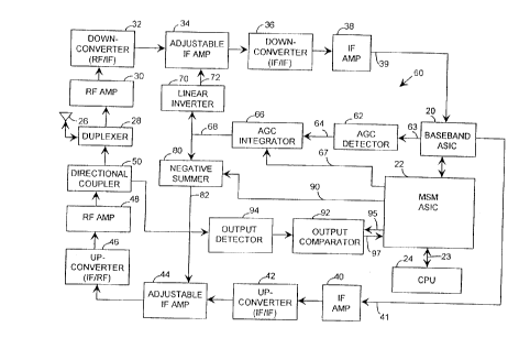
represent like components throughout the several views, FIG. I shows a block
diagram representation of portions of a code division multiple access (CDMA)
217S7 1~
13
spread spectrum ceilular radio telephone in accordance with a first preferred
embodiment of the present invention. Selected receiver and transmitter circuitalelements are connected to a baseband application-specific integrated circuit
(ASIC) 20, a mobile station modem (MSM) ASIC 22, and a central processing
unit (CPu) 24 which is connected to the MSM ASIC 22 through an address/data
bus 23. In accordance with the first preferred embodiment of the present
invention, the base~and ASIC 20 includes customary means for providing low
frequency analog processing and conversion of signals to and from the digital
domain for interfacing with the MSM ASIC 22. In partlcular, functions of the
baseband ASIC 20 include intermediate frequency (IF) to baseband conversion
(and vice-versa)l baseband and IF filtering, baseband signal quadrature splitting
and combining, baseband analog to digital and digital to analog conversion,
baseband direct current (DC) offset control, local oscillator quadrature generation,
and clock amplitude adjustments. Further in accordance with the first preferred
embodiment of the present invention, the MSM ASIC 22 conventionally provides
the majority of pllysical layer signaling through a demodulating unit, a decoding
unit, and an interleaving/deinterleaving unit. Arnong other functional elements, the
demodulating unit includes multiple path and searching receivers along with a
signal combiner; the decoding unit includes a viterbi decoder and data quality
verfication means; and the interleaving/deinterleaving unit includes a convo~utional
encoder, an interleaver, a deinterleaver, a psuedo-random number (PN) sequence
spreader, a data burst randomizer, and a finite impulse response (FIR) filter. In
addition to customary memory and support circuitry, the CPU 24 includes a
conventional static CMOS (complementary-symmetry metal-oxide-semiconductor)
high-integration microprocessor with general registers, segment registers, base
registers, index registers, status registers, and control registers.
The following describes examples of acceptable elements in accordance
with the first preferred embodiment of the present invention. Except for the
internal configuration modifications discussed herein (programming, etc.) prior art
examples of an accep~able CPU 24, MSM ASIC 22, and baseband ASIC 20 are,
21757~
respectively, the 80C186 microprocessor available from Advanced Micro Devices
of Sunnyvale, CA, the Q53 101- I S2 baseband ASIC available from Qualcomm,
Inc. of San Diego, CA, and the Q52501-lS2 MSM also available from Qualcomm,
Inc. Furthermore, it should be understood that the portions of the radio telephone
5 shown in FIG. I are only selected parts of the total cellular telephone which
includes a host o~ other components which, although not shown in any FIGS.,
would be readily understood by those skilled in the art regarding the operation of,
and the need for, such components. Furtherrnore, the circuital blocks shown
should be understood to primanly include elements prov1ding the named function
10 as well as customary filtering, noise reducing, and biasing circuitry.
As a radio signal is received through an antenna 26, a duplexer 28 directs
the signal to a radio frequency (RF) receiver arnplifier 30 which arnplifies thereceived signal before supplying it to a downconverter circuit 32 which convertsthe amplified RF signal into an IF signal. An adjustable gain IF receiver amplifier
15 circuit 34 receives and amplifies the IF signal before directing it to another
downconverter circuit 36 which converts the received IF signal into a lower
fre~uency IF signal. An IF receiver amplifier circuit 38 provides additional
amplification before the receiver IF signal is provided to the ba~eb~nd ASIC 20
through an IF input line 39. The baseband ASIC 20 also supplies a transmitter rF20 signal to an IF transmitter amplifier circuit 40 through an IF output line 41.- After
amplification, the transmitter signal is converted to a higher IF frequency through
upconverter 42 and then adjustably amplified through an adjustable gain IF
amplifier circuit 44. An upconverter cirulit 46 then converts the IF signal into an
RF signal which is then amplified by an RF amplifier 48. A directional coupler 50
25 passes the RF signal through to the duplexer 28 which directs the RF transmitter
output signal to the antenna 26 for final output.
Through continuous adjustment of the arnount of amplification provided by
the adjustable gain LF receiver amplifier circuit 34, the receiver IF signal is
maintained within a small range of variations for acceptable input into the b~ceb~nd
30 ASIC 20. Control of the adjustable gain IF receiver amplifier circuit 34 is
~1757 ~9
.
accomplished by an automatic gain control circuit (AGC) 60. An AGC detector
circuit 62 receives a representative IF signal through AGC input l;ne 63. As is
discussed in greater detail below, a direct current (DC) signal is output from the
AGC detector circuit 62 through an AGC detector output line 64 which represents
5 tlle strength of the received signal. An ACC integrator circuit 66 compares the
DC signal to a relatively constant AGC reference signal received over an AGC
reference line 67 from the MSM ASIC 22. The integrated difference between the
two signa]s is output onto an open loop output line 68 which is connected to a
linear inverter 70 suppling an AGC control signal to the adjustable gain 1~ receiver
10 amplifier circuit 34 over a re~eiver amplification control line 72. The linear
inverter 70 inverts the signal received over the open loop output line 68 to create
an inverse relationsllip between the received signal strength and the amount of
amplification provided by the adjustable gain IF receiver amplifier circuit 34.
Thus, for example, as received signal strength drops, the amount of amplification
15 provided by the adjustable gain IF receiver amplifier circuit 34 increases.
The open loop output line 68 also provides an input to a negative summer
circuit 80 which controls the adjustable gain IF transmitter amplifier circuit 44
through a transmitter amplification control line 82. In this way, the open loop
output line 68 provides the open loop component of the total output power control
20 so that the AGC integrator circuit 66 and AGC detector circuit 62 also contribute
to open loop gain control. One of the functions of the negative s--mmer circuit 80,
that of creating an inverse relationship between received signal strength and
arnplification, is similar to that of the linear inverter circuit 70. Thus, for example,
without regard to closed loop effects, as received signal strength drops, the
25 amount of amplification provided by the adjustable gain IF transmitter arnplifier
circuit 44 increases. Regarding closed loop control, the negati~lre s..m~er circuit
80 also receives input directly from the MSM ASIC 22 through a transmit gain
adjust line 90 As explained below, the transmit gain adjust signal on the transmit
gain adjust line 90 is an analog signal representing tl~e closed loop gain control
30 portion of total output power control as dictated by the tr~smitter amplification
- 21757 l9
,
16
control signal on the transmitter amplification control line 82. ~he-present
invention pertains primarily to the process of generating this transmit gain adjust
signal on the transmit gain adjust line 90
The transmit gain adjust signal on the transmit gain adjust line 90 is
5 generated by the MSM ASIC 22 in response to processes internal to the MSM
ASIC 22 as well as input received from the baseband ASIC 20, the CPU 24, and
an output comparator circuit 92. The output comparator circuit 92 receives inputfrom an output detector circuit 94 which receives input from the directional
coup~er 50. In general terms, the output detector circuit 94 generates a DC signal
10 representative of the total output power of the radio telephone. This DC signal is
compared inside the output comparator circuit 92 to a constant comparator
threshold voltage on line 95 generated by the MSM ASIC 22 as a representation ofan output power trigger le~el. The result of the continuous comparison is outputon line 97 from the output comparator circuit 92 to the MSM ASIC 22.
Refer now to FIG. 2 for a sche~ ic view of selected elements of FIG. 1.
The directional coupler 50 directs a small representative portion of the output
signal from the RF amplifier 48 through a pin labeled 0UT2. The signal flowing
from the OUT2 pin is received by the output detector 94 which generates a DC
signal represenlative of the total output power of the radio telephone. An AC-
coupling capacitor 100 removes any DC component from the signal outputfrom
tlle directional coupler 50. After filtering and conditioning by biasing resistors 102
and 104 and inductor 106, a diode 108 functions as a half-wave rectifier to convert
the remaining AC signal into a half-wave rectiSe~ signal. The output from diode
108 is smoothed and prepared for input tO the output comparator circuit 92 by
capacitors 110 and 114 and resistors 112, 116, and 118.
The output comparator circuit 92 receiYes the DC signal representative of
the total output power from the output detector circuit 94. The DC signal is
continuously compared through an operational amplifier 120 to a con~lant signal
set by the MSM ASJC 22. The constant signal is output through a comparator
threshold (COMP THRESH) output 131 of the MSM ASIC 22 before being
2175743
filtered and conditioned for input into the non-inverting input of the operational
amplifier 120. The COMP T~ESH signal is a pulse density modulated
representation of a comparator threshold register 130 located within the MSM
ASIC 22 and generated by a similarly located pulse density modulator (PDM) 132.
PDM 132 essentially provides a digital-to-analog conversion ofthe constant valuerepresented in the comparator threshold register 130, a digital memory element.
Since output from the output detector circuit 94 is directed into the
inverting input of the operational arnplifier 120, the operational amplifier outputs a
high signal into an input/output (I/O) port 133 of the MSM ASIC 22 as long as the
output from the output detector circuit 94 is lower than the fiitered and
conditioned constant output from the COMP THRESH output of the MSM ASIC
2''. This condition corresponds to the total output power of the radio telephonebeing below the output power trigger level. However, when the total output
power of the radio telephone rises above the output power trigger level, the
condition is indicated by a transition from high to low at the output of the output
comparator circuit 92. The output remains low until the output from the output
detector circuit 94 once again falls below the filtered & conditioned COMP
THRESH level, an event signifying that the total output power of the radio
telephone has fallen below the output power trigger level.
Through methods which are ~lisc-lssed in greater detail below, the MSM
ASIC 22 and CPU 24 utilize the signal levels detected from the output comparator92 to modify a closed loop power control register (CL PWR CTl~L REG) 140
located within the MSM ASIC 22. Like the comparator threshold register 130 and
PDM 132, a PDM 142 provides an analog ~e~res~ tion of values stored in the
closed loop power control register 140. This analog ,~plesenlation is output
through a transmit gain adjust (TX GAIN ADI) output 150 of the MSM ASIC
onto the transrnit gain adjust line 90 which is connected to the negative sumrner 80
shown in FIG. 1. An AGC reference output 152 is also shown supplying the AGC
reference signal onto the AGC reference line 67. The MSM ASIC 22 also includes
a control bit (CB) 143 located in another area of MSM ASIC 22 mernory which is
-- 217~7~
18
writeable by the CPU 24 and which controls whether the CPU 24 controls the
closed loop power control register 140 or the MSM ASIC 22 controls the closed
loop power control register 140 through conventional closed loop power control
techniques.
The baseband ASIC 20 is shown supplying a representative receiver IF
signal onto the AGC input line 63 through a receiver IF output (RX IF OUT) to
the AGC detector 62. The representative receiver IF signal is examined by the
AGC detector 62 to yield on the AGC detector output line 64 a DC representation
of the received signal strength. A capacitor 170 blocks any DC component of the
signal on the AGC input line 63. Biasing elements 172, 1 ~4, 176, 178, and 180 are
sized to bias a bipolar transistor 190 in the active amplification ~e~iOn so that a
constant amount of gain is applied between the base and the collector of the
bipolar transistor 190 which is connected to the amplified line 192. The amplified
line 192 is connected to a capacitor 200 which is further connected to the cathode
of a diode 202 with a grounded anode and to the anode of diode 204. The cathode
of the diode 204 is connected to a grounded resistor 206 and a resistor 210 which
is connected to the AGC detector output line 64 along with a grounded capacitor
212. Since capacitor 200 is coMeeted in series (AC-coupled) with subsequent
elements, capacitor 200 removes the r)C component from the AGC input signal
and cooperates witl1 the diodes 202, 204 to add a new DC level to the AC -
component which is linearly proportional to the incoming AC signal level. As theAC signal level rises, the capacitor 200 is charged, and when the AC signal level
falls, the diode 202 turns on, resulting in an upward voltage shiP~. Resistor 210
and capacitor 212 function as a low pass filter to remove the l em~ AC
component to leave a DC signal which is linearly proportional to the AC signal
level of the AGC input signal. In addition, the resistor 210 functions as an
averaging means to slow the charge of capacitor 212 so that the AGC output
signal on the AGC detector output line 64 is an averaged linear output.
Furthermore, the resistors 206 and 210 are preferably approximately equal in
value.
2175749
.
19
Refer now to FIG. 3 for a schematic view of the AGC integrator circuit 66,
the linear inverter 70, and the negative summer 80. The AGC detector output line
64 is shown supplying signals through a biasing resistor 220 to the non-inverting
input of an operational amplifier 222, which input is also connected to biasing
S components 220, 226, and 228. The AGC REF line 67 is sho~vn providing the
relatively constant AGC reference signal through a networ3c of biasing elements
230, 232, 234, and 236 to the inverting input of the operational amplifier 222. The
output and inverting input of the operational amplifier 222 are shown connected
through a capacitor 238 so that the operational amplifier 222 fi~nctions as an open
10 loop integrator to produce a gain control signal on the open loop output line 68
eclual to the difference between the signal levels on the AGCI d~tec~or output line
64 and the AGC REF line 67. The linear inverter 70 is shown reeeiving the gain
control signal on the open loop output line 68 and providing output through the
receiver amplification control line 72. The open loop output line 68 is shown
15 connected through a resistor 250 to the inverting input of an operational amplifier
252. A resistor 254 is shown connected between the output and inverting input of
the operational amplifier 252, whereas the non-inverting input of the op arnp 252 is
grounded through a network of biasing elements 257, 258, and 259. Thus, the
operational amplifier 252 functions as an inverting amplifier operating in a linear
20 manner without undue complexity.
The negative summer 80 is shown receiving open and closed loop signals
through the open loop output line 68 and the transrnit gain adjust line 90,
respectively. A~er passing through biasing/filter networks composed of resistor~
270, 272, 274, 280, 282, and 284, signals are combined from the open loop output
25 line 68 and the transmit gain adjust line 90 at the inverting input of an operational
amplifier 300. The biasing filter networks (270 - 284) exhibit time cor.s~ l delays
appropriate for ensuring stable operation. According to the first preferred
embodiment of the present invention, the delays introduced are applo~...ately
30ms on the open loop output line 68 and 0.5ms on the transmit gain adjust line
90. The operational amplifier 300 is biased, through elements 302, 304, 306, 308,
-- 21757~
320, and 322 to amplify and invert the sum of the two input signals and provide
output on the transmitter amplification control line 82. Thus, it is through theoperational amplifier 300 that both closed loop gain control and open loop gain
control components are combined to control total output power of the radio
telephone.
FIG. 4 is a flow chart represcntation of a power control process for the
elements shown in FIG. 1, in accordance with one preferred embodiment of the
present invention. Referring primarily to FIG. 4 with additional reference to FIGS.
l and~2, a~er the process starts in step 400, the VO port 133 is configured to be a
general purpose VO port which is readable by the CPU 24 in step 402, unless
already configured as such. Subsequently, according to step 40~, conventional
closed loop control of the closed loop power control register 140 by the MSM
ASIC 22 is initiated by the CPU 24. According to this first preferred embodimentof the present invention, the process of step 404 includes initi~ in~ the control bit
143 in the state allowing normal MSM ASIC 22 control of the closed loop power
control register. Subsequently, the VO port 133 is read by the CPU 24 in step
406. If the VO port 133 is found to be receiving a high signal (e.g., +5 volts), the
NO branch of decision block 408 directs operation to step 410 where conventionalclosed loop control of the closed loop power control register 140 is maint~ined
(i.e., the control bit 143 is le~ un~-h~nged). Then, a delay step 412 indicates that
the process of FIG. 4 delays for a predetermined amount of time before operationrepeats back to step 406. According to this first preferred embodiment of the
present invention, this delay corresponds to the period of time between receiving
closed loop power control i"~l"~,tion from the base station, such as 1.25 ms. Inthis manner, a first mode of operation is m~int~ined while the VO port 133 is high,
indicating that the total output power of the radio telephone is below the output
power trigger level. Another reason for the delay in the present invention is toallow changes in power control to take effect prior to reading the VO port 133
again.
CA 0217~749 1999-01-29
On the other hand~ when the total output power of the radio telephone exceeds
the output power trigger level, the output comparator 92 outputs a low si~nal onto the
S I/O port 133. Through the YES branch of decision block 408, operation proceeds to
step 414 as a second mode begins to prevent power control saturation and limit
maximum output power of the radio telephone. At step 414, the CPU 24 modifies the
control bit 143 to enable saturation prevention control ofthe closed loop power
control register 140~ thus disabling conventional closed loop power control of that
register. Subsequently. the CPU 24 automatically modifies the closed loop power
control register 140 to decrement the total output power of the radio telephone by one
step. In this preferred embodiment of the present invention, this process includes
incrementing the value stored in the closed loop power control register 140 by one
step, corresponding to a I dB reduction in total output power. In one implementation
of the first preferred embodiment of the present invention, the closed loop power
control register includes the seven most significant bits of an eight-bit re,~ister~ thus
providing 128 total steps of control (64 bits above the open loop estimate and 64 bits
below lhe open loop estimate). This increased range of closed loop control provides
additional ability to accommodate production variances~ etc.
After step 416~ the delay step 412 indicates another delay before operation
again continues with step 406 so that the l/O port 133 is continually read by the
CPU 24. The saturation prevention mode continues through repeated loops
through the YES branch of decision block 408 so that the closed loop power
control register 140 is continually incremented (decrementing total output power)
until the total output power falls below the output power trigger level. V~ hen this
happens, the NO branch of decision block 408 directs operation back to step 410
where conventional closed loop operation resumes. In many circumstances.
only one loop through the YES branch of decision block 408 is necessary before
alternating back to the NO branch. However~ since the open loop gain control
3() system conlribution to the total output power may also rise, consecutive loops
through the YES branch of decision block 408 are also encountered where the
~'1757 19
total output power is continually decremented until it ~alls below the output power
trigger level.
FIG 5 is a flow chart representation of a power control process for the
eiements shown in FIG. 1, in accordance with a second preferred embodiment of
5 the present invention. A~er starting in step 420, this second power control
method includes configuring the I/O port 133 as an edge-tnggered interrupt port
rather than a generai purpose readable VO port. In this configuration as an edge-
triggered interrupt port, the MSM ASIC I/O port 133 is not continually examined
by the CPU 24. Instead, the MSM ASIC 22 notifies the CPU 24 when the signal
10 output frorn ~he output comparator 92 changes from a high signal to a low signal,
thus signifying that the total output power of the radio telephone has exceeded the
output power trigger level. Thus, the output comparator signal at the I/O port 133
is essentially ignored by the CPU (saving CPU resources) as long as the total
output power is below the output power trigger level. As shown in steps 424 and
1 S 426, aPter conventional closed loop control of the closed loop power controlregister 140 is enabled, the CPU 24 continues with other processing during this
first conventional mode of closed loop power control.
As transition from high to low on the VO port 133 is detected at step 428,
an intern~pt service routine is initiated in the CPU 24. Control of the closed loop
20 power control register 140 then shif'~s from conventional closed loop control by the
MSM AS1C 22 to saturation prevention control by the CPU 24 in step 430. The
closed loop power control register 140 is then modified in step 432 to decrementthe total output power by one step (1.0 dB) before the l/O port 133 is
reconfigured to be a readable port. Of course, depending on availability, separate
25 MSM ASIC ports can also be utilized for interrupt and re~ding functionality.
Then, like the method of the first preferred embodiment, steps 436 - 444 indicated
that while the total output power remains above the output power trigger level, the
CPU 24 continues to modify the closed loop power control register 140 to
decrement the total output power until the total output power falls below the
30 output power trigger level. When this happens, as detected by decision block 438,
217~7 19
..
the interrupt service routine terminates by again configuring the IIO port 133 as an
edge-triggered interrupt port and enabling conventional closed loop control of the
closed loop power control register 140.
FIG. 6 shows a ~low chart representation in accordance with yet another
5 preferred embodiment a power control process for the elements shown in FIG. 1.APter starting in step 460, the process of FIG. 6 includes configuring the I/O port
133 at step 462 to be a level-triggered interrupt port. An interrupt port of this
type is essentially ignored until the input signal reaches a trigger level, such as, in
this c'ase, a low signal from the output comparator 92. AP~er enabling conventional
closed loop control of the closed loop power control register 140 in step 464, the
CPU 24 continues with other processing in step 466 until a leve~-triggered
interrupt signa1 is generated from the I/O port 133 and detected at step 468 to
begin an interrupt service routine. Saturation prevention control of the closed loop
power control register 140 begins in step 472. The closed loop power control
register 140iS then modified to decrement the total output power by one step
before the closed loop power control register 140 is immediately returned to
conventional closed loop power control in step 476. A~er a subsequent delay in
step 478, the interrupt servicing routine terminates with processing looping back to
step 466. Since saturation prevention control of the closed loop power control
register 140 has a very short duration, all power control irlformation from the base
station affects the closed loop power control register 140, unlike previously
discussed methods. Thus, if the next base station power control information
received by the radio telephone during the delay is another increase power
instruction, the interrupt service routine will likely be triggered immedi~tely after
step 478, depending on changes in the open loop component of the total output
power.
Refer now to FIG. 7 for a block diagram representation of portions of a
radio telephone in accordance with another preferred embodiment of the present
invention. The elements of FIG. 1 are, independent of programming and memory
configurations of MSM ASIC 22' and CPU 24, identical to those of FIG. 1 except
217~7~
24
for the omission of the output comparator 92 of FIG. I and the addition of an
analog-to-digital (A-to-D) converter 500 connected between the output detector
94 and the addresslbus 23 ~or direct communication with the CPU 24. While the
c!osed loop power control register 140 and control bit 143 (FIG. 2) also exist in
the MSM ASIC 22', the comparison threshold register 130 and associated PDM
132 and output port 133 of the first preferred embodiment are not included as
such. Furthermore, instead of, as in the first preferred embodiment, continuously
comparing a detected DC representation of the total output power to a constant
DC lèvel through an operational amplifier, the radio telephone ofthe preferred
embodiment represented by FIG. 7 continually sarnples output power through the
A-to-D conver~er 500. The digital s~rnples are input directly ~o the CPU 2~' where
tlley are compared to a stored representation of the output power trigger level.FIG 8 shows a flow chart representation of a power control process for
the radio telephone embodiment represented by FIG. 7. Referring to steps 520 -
530, as with the first preferred embodiment of the present invention, until the total
output power is found to rise above the output power trigger level, the closed loop
power control register 140 is controlled according to the conventional closed ~oop
gain control mode. Likewise, referring to steps 532 and 534, when the total
output power is detected to be too high (above the output power trigger level), the
CPU 24 enters a saturation prevention mode to assume control of the clos~d loop
power control register 140 and modif~r it to reduce the total output power until the
total output power falls below the output power trigger level. One example of anacceptable A-to-D converter 500 is the MAX 153 available from Maxim
Integrated Products of Sunnyvale, C~
Yet another preferred embodiment of the present invention is disclosed in
FIGS. 9 and l 0. The block diagram I ~prese,1talion of FIG. 9 represel.ls a radio
telephone which is extremely similar to that of FIG. I ~ The primaly dif~erence
between FIG. I and FIG. 9 is the addition of a received signal strength indicator
(RSSI) detector 552 connected to the open loop output line 68 through an RSSI
input line 550. One example of an acceptable RSSI detector 552 is the same
CA 0217~749 1999-01-29
.
device given as an example for the A-to-D converter 500 above. The MSM ASIC 22"
and CPU 24" are also modified to utilize the RSSI detector 552 as a factor in output
power control. The process of FIG. 10 is very similar to that of FIG. 4 in that steps
560 - 572 are identical to steps 400 - 408. If a low signal is detected through the I/O
port 133, the process is delayed through step 574 and controlled in a loop back to step
570. Otherwise, the YES branch of decision block 572 directs operation to step 580
where saturation prevention control of the closed loop power control register 140 is
enabled. At step 582 a received signal strength indication is read from the RSSIdetector 552 and stored by the CPU 24".
Subsequently. at step 584, the power control process waits for closed loop
control information from the base station requesting the radio telephone to decrease
output power. Until such a decrease power instruction is received, the NO branchretains operation in a loop through step 590. Step 590, including an internal delay of
one instruction period (e.g., 1.25ms), represents a continual comparison of a current
RSSI with that stored by the CPU 24 in step 582 along with a contingent modification
of the closed loop power control register 140 in the MSM ASIC 22". If the received
signal strength does not decrease during this loop, no modification is made to the
closed loop power control register 140. On the other hand, if the RSSI decreases, the
closed loop power control register 140 is modified to compensate for the change. In
other words, if the open loop component of the total output power rises, the closed
loop power control register is used to compensate. This process utilizes a relative
look-up table technique performed by the CPU 24" in determining how much to
modify the closed loop power control register 140. Another acceptable technique
includes an absolute value look-up table which determines the appropriate value for
the closed loop power control register 140 as an absolute function of the received
signal strength. as opposed to determining relative differences.
This process continues until a decrease power instruction is received from
the base station, directing operation through the YES branch of decision block
584 to step 592. The process of step 592 includes the actions of step 590 (expect the
217S749
internal delay) as well as the additional factor of the decrease power instruction.
Thus, the modification to the closed loop power control register 140 of step 592includes an additional one step (1.0 d~) reduction of output power because of the
decrease power instruction. One additional requirement imposed on the MSM
5 ASIC 22" is that base station closed loop power control instructions be available to
the CPU 24". Sucl1 is not the case with the prior art example MSM ASIC 22 from
Qualcomm, thus the present invention needs an MSM ASIC 22" which is so
modified from tllat example. One alternative to the metllod of this preferred
embodiment, as well as to other pref~lled embodiments disclosed herein, would be10 to provide another alternate MSM ASIC which internaliy performed all of the
steps of any one of the disclosed processes without CPU 24 involvement A~er
step 592, conventional closed loop control of the closed loop power control
register is enabled in step 594, and a delay is imposed in step 596 before the
process loops back to step 570.
FIGS. l 1 and 12 pertain to still another preferred embodiment of the
present invention. The primary differences between the preferred embodiment of
FIGS. 11 and 12 and the preferred embodiment of FIGS. 9 and 10 are related to
the means for deterrnining when the total output power is above the output powertrigger level. The previous preferred embodiment (FIGS. 9 and 10) utilizes an
output detector 94 and an output comparator 92 similar to that of the first -
preferred embodiment. On the other hand, the present preferred embodiment
(FIGS. 11 and 12) utilizes an RSSVoutput detector 600 connected through a
multiplexer 602 to both the output detector 94 and the open loop output line 68.Through the multiplexer 602, as controlled through a multiplexer selector control
line 601, the RSSI/output detector 600 is able to, in cooperation with the CPU 24"'
and MSM ASIC 22"', pe~ the function of both the A-to-D converter 500 of
FIG. 7 and the RSSI detector 552 of FIG. 9. rhus, as shown in FIG. 12, the
process of the represented preferred embodiment is almost identical to that
represented by FIG. 10 except for changes due to using an analog-to-digital
sarnpling source for output power determination.
217~749
Finally, in light of the variances in open loop power, it should be
understood that the term "maximum power" and similar terms used herein refer to
one of a small range of total output power levels above the output power triggerlevel. Similarly, the scope of the present invention includes additional preferred
5 embodiments which include multiple output power trigger levels based upon
various communication modes. For example, in certain communication modes, the
conventional closed loop power control step may be larger than 1.0 dB, thus the
threshold amount would need to be lower to appropriately limit output power for
that rnode of communication.
While the embodiments of the present invention which have been disclosed
herein are the preferred forms, other ernbodiments of the present hlvention willsuggest themselves to persons skilled in the art in view of this disclosure.
Therefore, it wil] be understood that variations and modifications can be ef~ected
within the spirit and scope of the invention and that the scope of the present
15 invention should only be limited by the claims below. Furthermore, the equivalents
of all means- or ste~plus-function elements in the claims below are intended to
include any structure, material, or acts :for performing the function as specifically
claimed and as would be understood by persons skilled in the art of this disclosure.