Note: Descriptions are shown in the official language in which they were submitted.
21 77664
DIGITAL JKECEIVE FILTER FOR COMMUNICATIONS SYSTEMS
This invention relates to a filter for a communications system, and is
particularly
concerned with filtering at the; receiver of the system by what is termed a
receive filter.
Background of the Invention
It is well known to communicate digital signals via a communications path
using a
transmitting modulator and a :receiving demodulator which operate in
accordance with a
desired modulation scheme. By way of example, Tomlinson et al. United States
Patent
No. 4,961,206 issued October 2, 1990 and entitled "Data Modem System"
describes a
communications system using; QPSK (Quadrature Phase Shift Keying) modulation
with
eight times oversamhling of the binary signal to be communicated.
At the modulator or transmitter of such a system, the signal is digitally
filtered in a
transmit filter and modulated to form phase quadrature components which are
converted
by a digital-analog (D/A) converter to be applied to the communications path.
The
transmit filter is conveniently implemented by a look-up table in ROM (Read
Only
Memory), which can be arranged simultaneously to perform the modulation
function in an
eight times oversaml>led system. At the receiver or demodulator of the system,
the
received analog sign<il is converted to a digital signal by an analog-digital
(A/D) converter
and demodulated to produce received signal components which are digitally
filtered by the
receive filter and processed to recover the original signal. The receive
filter can also be
implemented by a look-up table in ROM.
As is well known, the transmit and receive filters are designed to provide a
composite filter amplitude response which is flat in the pass band to minimize
distortion,
has a raised-cosine shape in the transition band (typically with 20 to 30%
excess
bandwidth) to minimize inter-symbol interference (ISI), and has a large
attenuation in the
stop band to minimize adjacent channel interference (ACI). As described in the
Tomlinson
et al. patent, the desired specta-al shaping is divided equally between the
transmit and
receive filters for optimum system performance.
A problem with such a system is that, whereas for each of the quadrature
phases
the transmit filter is supplied with a single bit of the binary signal per
modulation symbol,
the receive filter is supplied with a multiple-bit output from the A/D
converter; for example
this may comprise 6 bits, as described in the Tomlinson et al. patent, or 8
bits per symbol.
Consequently, the RUM constituting the receive filter must be a multiple of
(26 or 2g
times) the size of the transmit filter ROM. For a high bit rate, for example
2.56 Mb/s, of
the binary signal a desired performance may require a 63-tap FIR (finite
impulse response)
transmit filter. A similar receive filter for accommodating multiple bits per
symbol
becomes undesirable or impractical in terms of ROM size for a look-up table
filter, speed
for a DSP (digital signal proccasor) implementation of the filter, and/or
costs.
A
21 X7664
2
An object of this invention is to provide a simplified digital filter for use
as a
receive filter in a communicaKions system.
Summar~r of the Invf:ntion
According to this invention there is provided a digital receive filter for a
communications sysoem, the i:ilter comprising a first filter part for
filtering samples at a
first frequency, a down sampler for down sampling an output of the first
filter part by an
integer down sampling factor L, and a second filter part for filtering samples
from an
output of the down sampler at a second frequency equal to the first frequency
divided by
L, wherein at least the second. filter part comprises a plurality of cascaded
filter stages,
each filter stage of the second filter part comprising a second order finite
impulse response
digital filter having symmetrical coefficients comprising a middle coefficient
the magnitude
of which is either zero, an integer power of two, or a sum of a plurality of
integer powers
of two, and two further coefficients the magnitude of each of which is an
integer power of
two.
The implementation of such a filter is facilitated by making the middle
coefficient
of each of a majority of the filter stages an integer power of two. Each of
the majority of
filter stages can then comprise: a latch for latching an input sample, a first
delay unit for
delaying an output o:f the latch by one sample period, a first add unit for
adding an output
of the first delay unit and an output of the latch, a second delay unit for
delaying an output
of the first add unit by one sample period, and a second add unit for adding
an output of
the second delay unit and an output of the latch. Integer power of two
coefficients are
then effected by shifting of bits supplied to the inputs of the add units. The
other filter
stages can be similar except for omission or duplication of the first add
unit. In this way,
the filter stages are greatly simplified by not requiring any multiplier
units.
The symmetrical coefficients of each filter stage are preferably products of a
scaling factor A which is an integer power of two and normalized symmetrical
coefficients
1 B 1 of the filter sta;;e. The normalized middle coefficient B of one of the
filter stages
can be negative with a magnitude greater than 2, whereby this filter stage
provides a gain
which increases with increasing frequency to compensate for slope in the pass
band of the
other filter stages which have normalized middle coefficients B with
magnitudes that are
positive, zero, or less; than two. This one of the filter stages is desirably
positioned
among the cascaded :filter stages nearer to an output than to an input of the
filter for
optimum filtering of noise.
The first filter part preferably comprises a plurality of cascaded filter
stages, each
filter stage of the first filter part comprising a second order finite impulse
response digital
filter having symmetJ-ical coefficients comprising a middle coefficient the
magnitude of
which is an integer power of two, and two further coefficients the magnitude
of each of
which is an integer power of two.
2177664
3
Brief Description of the Drawines
The invention will be: further understood from the following description with
reference to the accompanying drawings, in which:
Fig. 1 scherr~atically illustrates a block diagram of a two-part receive
filter which
S uses cascaded filter stages in accordance with the invention;
Fig. 2 scherr~atically illustrates a basic form of a filter stage used in a
receive filter
in accordance with an embodiment of the invention;
Fig. 3 schematically illustrates an arrangement of a receive filter as
illustrated in
Fig. 1 comprising cascaded filter stages as illustrated in Fig. 2 in
accordance with an
embodiment of the invention; and
Fig. 4 schematically iillustrates a modified form of the filter stage of Fig.
2 for use
as one of the filter stages of the receive filter of Fig. 3.
Detailed Description
The invention is described below by way of example in its application to a
system
in which a binary si;;nal having a bit rate of 2.56 Mb/s is communicated, for
example via a
cable television distribution network, using DQPSK (differential QPSK)
modulation at a
symbol rate corresponding to a frequency of 10.24 MHz. In such a system, pairs
of bits
(dibits) of the binary signal are eight times oversampled and modulated as a
differential
phase of the two quudrature phase corners at one quarter the sampling rate;
this facilitates
implementation of the modulator in that the interpolation, transmit filtering,
and
modulation functions can be constituted by using look-up tables in ROM.
However, it
should be appreciated that thcae details are given only by way of example and
to facilitate
understanding of the; invention, and that the invention is also applicable to
other systems,
modulation schemes, and communication rates.
After D/A conversion in the transmitter, analog filtering at the transmitter
and
receiver for communication of the analog signal via the communications path,
and A/D
conversion in the re~;eiver, h~umonic images of the digital DQPSK spectrum
exist at center
frequencies of (2.56 + 5.12rn) MHz, where m is zero or a positive or negative
integer.
Using the sampling rate of 10.24 MHz facilitates demodulation, which results
in desired
signal components at center lFtequencies of 0 and 10.24 MHz and an undesired
harmonic
image at a center frequency of 5.12 MHz after quadrature mixing. The receive
filter is
desired to perform digital low pass filtering to remove this harmonic image
and ACI. For
30% excess bandwidth this requires a stop band cut-off frequency of the filter
of
1.3 x 1.28 / 2 = 0.8;12 MHz and suppression, i.e. high attenuation, of the
harmonic image
at 5.12 MHz.
A high-order filter is required to meet these requirements directly. In
addition, as
explained in the introduction., it is conventional to divide the system
filtering requirements
equally between the transmit and receive filters. As a result of these
considerations and
2717664
4
the fact that the receive filter operates on the multiple-digit output of the
A/D conversion
process, the receive filter becomes very complex.
This disadvantage is avoided in the embodiment of the invention described
below
in the following ways. Firstly, the required order of the filter is lowered to
a large extent,
while achieving the same filtering results, by using mufti-rate signal
processing techniques
in which the filter is divided into different filter parts. Secondly, these
filter parts are
designed to be implemented using simple filter stages in cascade. These steps
result in a
receive filter that has approximately, but not exactly, the desired response
for an equal
division of filtering between l:he transmit and receive filters. The transmit
filter is then
designed to match the receive; filter, i.e. to provide, in cascade with the
actual response of
the receive filter, the particular desired combined filter response for the
system.
More particularly, the use of mufti-rate signal processing techniques divides
the
filter into two parts ~avith decimation, or down sampling, between the
successive parts.
The first part of the i°ilter operates at the sampling frequency of
10.24 MHz, and the
second part operates on the decimated sequence at a frequency of 10.24 / L MHz
where L
is the decimation or down sampling factor. Although not further described
here, the same
techniques can be used to divide the filter into more than two parts, with
down sampling
between each pair of successive filter parts, the filter parts all operating
at successive
lower frequencies.
Fig. 1 illustrates a receive filter comprising two digital LPF (low pass
filter) parts
10 and 12 arranged i n this manner, with a down sampler 14 between the two
parts. An
objective is to distribute the filtering load between the LPF parts 10 and 12
so that filtering
is computationally e~=ficient.
In the embodiment of the invention described below, in order to perform as
little
processing as possible at the lhigher sampling rate of the LPF part 10, this
is implemented
as a relatively simple LPF in order to suppress the harmonic image at 5.12
MHz, and the
LPF part 12 operating at a lower rate is implemented as the main filter for
suppressing
ACI. The down sampling facaor L of the down sampler 14 is selected to be 2, so
that the
LPF part 12 operate; at the same frequency, 5.12 MHz, as the removed harmonic
image.
The LPF part 10 is implemented as a 5-tap FIR filter, and the LPF part 12 is
implemented
as a 15-tap FIR filter, the two parts providing a composite frequency response
equivalent
to that of a 33-tap filter.
Each of the LPF parts. 10 and 12 is constituted by a plurality of cascaded
second
order FIR filter stagers having symmetric coefficients; generally the stages
each have a
simple basic form and implementation as illustrated in Fig. 2.
Refernng to Fig. 2, each filter stage comprises a latch 20, two delay units 22
and
24 each providing a ~~elay of one sample time T at the operating frequency of
the filter
stage, and two add units 26 and 28. It can be appreciated that in a DSP
implementation of
2177664
the filter stage, these: would all be constituted by functions of the DSP. The
latch 20
serves for latching each input signal sample to the filter stage, and its
output is coupled to
an input of the delay unit 22 and a first input of each of the units 26 and
28. The unit 26
has a second input coupled to. an output of the delay unit 22, and an output
coupled to an
5 input of the delay unit 24. The unit 28 has a second input coupled to an
output of the
delay unit 24, and aru output constituting an output of the filter stage.
Each sample incoming to the filter stage is denoted X(n), with the preceding
two
samples being denoted X(n-1) and X(n-2) respectively, where n represents a
sample
number and X represents the value of the sample, which comprises multiple, for
example
at least eight, digits. Generally, each coefficient of the filter stage is an
integer power of
two, and is accomplished by coupling the bits of the respective sample to the
bit lines of
the respective input of the unit 26 or 28 with an offset corresponding to the
coefficient.
Equivalently, and as would be the case for a DSP implementation, each
coefficient is
implemented by a left-shifting or right-shifting of the bits of the respective
value. For
example, a left-shift by one or two bit positions implements a coefficient of
2 or 4
respectively, a right-shift by one or two bit positions implements a
coefficient of 1/2 or 1/4
respectively, and no shift implements a coefficient of 1. In addition,
negative coefficient
values are produced by twos-complement coefficient values in known manner.
Consequently, each filter stage can be seen to have a function of the general
form
Y(n) = A ( X(n) + B X(n-1) + X(n-2) )
where Y(n) represents the output of the filter stage; A = 2S, where s = 0, ~1,
~2 ..., is a
scaling (or gain) factor; and l3 = ~2k, where k = 0, ~l, ~2 .. ., is a
normalized middle
coefficient of the filter stage, i.e. the value of the middle coefficient, of
the term X(n-1),
when the other two coefficients, of the terms X(n) and X(n-2), are 1.
Exceptions to the above generality are described below. In one case, the
middle
coefficient is zero; in this case: the unit 26 (or its DSP function) is
omitted from the filter
stage. In another case, the muddle coefficient is not an integer power of two
but is a sum
of two different inte;~er powers of two; in this case the unit 26 (or its DSP
function) is
duplicated in the filtf:r stage. Obviously this principle could be extended to
filter stages
having middle coefficients wlhich are sums of more than two different integer
powers of
two, with correspondingly more add units in the filter stage.
A filter stage as illusb°ated in Fig. 2 can, for example, have a
scaling factor A = 1/4
(i.e. s = -2) and a normalized middle coefficient B = 2 (i.e. k = 1), so that
its function is:
Y(n) = 1/4 X(n) + 1/2 X(n-1) + t/4 X(n-2)
with symmetrical coefficients t/4 1/2 1/4. This would be implemented in the
filter stage by
a coefficient of 1/2 (rzght-shift by one bit position) at the first input of
the unit 26 from the
latch 20; a coefficient of 1/4 (right-shift by two bit positions) at the
second input of the unit
26 from the delay unit 22 and at the first input of the unit 28 from the latch
20; and a
2111664
6
coefficient of 1 (no shift) at the second input of the add unit 28 from the
delay unit 24.
The sum of the coefficients represents gain through the filter stage, and in
this case is 1.
In order to accommodate the ahifting of the input signals at the inputs of the
units 26 and
28 without introducvig quantizing noise, these units must have a greater bit-
capacity than
the signal samples being filtered. For example, the units 26 and 28 can be 12-
bit adders
for 8-bit input signal samples to the filter.
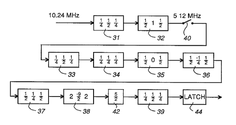
Fig. 3 illustrates a complete receive filter, comprising 9 filter stages 31 to
39 each
of which is represented as a rectangle with the symmetrical coefficients of
the filter stage
being shown within t:he respective rectangle. The receive filter further
comprises a
sampling switch 40 which constitutes the down sampler 14 of Fig. 1, a gain
stage 42 as
described further below, and an output latch 44.
As described above, the LPF part 10 operates at the sampling rate of 10.24 MHz
and is implemented as a relalavely simple LPF in order to suppress the
harmonic image at
5.12 MHz. It consists of the two cascaded filter stages 31 and 32 each as
described above
with reference to Fig. 2, the filter stage 31 having a scaling factor of A =
1/4 and the filter
stage 32 having a scaing factor or gain of A = 1/2. Both of the filter stages
31 and 32
have a normalized middle coefficient of B = 2. The gains (sums of the
coefficients) of the
filter stages 31 and 32 are therefore 1 and 2 respectively, for a total gain
of 2 through the
filter part 10. This compensates for the fact that, as a result of
demodulation in
accordance with the modulation scheme described above, alternate samples of
the
respective one of the phase quadrature signals supplied to the filter are
zero.
The signal samples are down sampled by the factor of L = 2 by the switch 40
constituting the down sampler 14, so that the remainder of Fig. 3 operates at
a sampling
frequency of 5.12 MHz. This constitutes the LPF part 12 which comprises the 7
~ cascaded filter stages 33 to 39, with the additional gain stage 42 which
provides a gain
factor of 21/2. The filter stages 33, 34, 36, 37, and 39 are each exactly as
described
above with reference to Fig. 2'., with their respective scaling factors A and
normalized
middle coefficients >=t. The filter stage 35 differs from these stages in that
its normalized
middle coefficient B is zero, s~o that in this filter stage the function of
the add unit 26 of
Fig. 2 is dispensed with and tl~e output of the delay unit 22 is connected
directly to the
input of the delay unit 24.
The filter stale 38 also differs from the other stages in that it has a
normalized
middle coefficient of B = -21/'4, the magnitude of which is not an integer
power of two but
is a sum of two integer powers of two (2 and 1/4). Accordingly, in this filter
stage 38 the
add unit 26 of Fig. 2 is duplicated by an extra add unit 27 to provide this
sum as
illustrated in Fig. 4. Fig. 4 also illustrates an implementation of the gain
stage 42, which
is connected immediately following the filter stage 38, by a further add unit
also
referenced 42.
_. 2117664
7
Refernng to Fig. 4, The filter stage 38 consists of the latch 20, delay units
22 and
24, and add units 26 and 28 ass described~above with reference to Fig. 2, with
the extra
add unit 27 inserted between the units 26 and 24 and having a first input
coupled to the
output of the latch 2~0, a second input coupled to the output of the add unit
26, and an
output coupled to the input oiF the delay unit 24. The first and second inputs
of the add
unit 26 have weightings of -4- (twos-complement and left-shift two bit
positions) and 2
(left-shift one bit position) respectively, as indicated by these numbers
adjacent the input
lines of this add unit. The first input of the add unit 27 has a weighting of -
1/2 (twos-
complement and right-shift one bit position) as indicated by this number
adjacent its input
line, and the second input has a weighting of 1 (no shift). The first input of
the add unit
28 has a weighting of 2 (left-shift one bit position) as indicated by this
number adjacent its
input line, and the second input has a weighting of 1 (no shift). The add unit
42 has both
its inputs coupled to the output of the add unit 28 of the filter stage 38
with weightings of
2 (left-shift one bit position) and 1/2 (right-shift one bit position) as
indicated by these
numbers adjacent its input lines, to provide the desired gain factor of 21/2.
The scaling factors A,, normalized middle coefficients B, symmetrical
coefficients,
and gains of the cascaded filter stages 31 to 39 and the gain stage 42 are
summarized in
the following table:
Scaling Normalized
LPF PartStage Factor Middle Symmetrical CoefficientsGain
A Coeff.
B
10 31 1/4 2 1/4 1/2 1/4 1
32 1/2 2 1/2 1 1/2 2
33 1/4 2 1/4 1/2 1/4 1
34 1/4 1 1/4 1/4 1/4 3/4
35 1/2 0 1/2 0 1/2 1
12 36 1/2 -1/2 1/2 -1/4 1/2 3/4
37 1/2 1/2 1/2 1/4 1/2 11/4
38 2 -21/4 2 -41/2 2 1/2
42 __ - - - - 5/2
39 1/4 2 1/4 1/2 1/4 1
It can be seen from this table that the gain of the gain stage 42 is selected
to make
the total gain througlh the LPF part 12 also about 1 (actually 225/256). The
order in which
the filter stages (and gain stage) of each of the LPF parts 10 and 12 are
cascaded is not
significant to the filt~~ring function itself. However, this order affects the
sample
magnitudes, and hence the rewired bit-capacity of the filter stages for
reducing noise, so
that the order illustrated in Fig. 3 and described above is preferred.
2117664
In the above respect it is observed that the filter stage 38 is optimally
positioned
towards the end of the cascaded filter stages of the LPF part 12 rather than
towards the
beginning. This is t~ecause the normalized middle coefficient B of the filter
stage 38 has a
magnitude greater than 2, as a result of which the gain of this filter stage
increases with
frequency so that it has a high gain for noise frequencies above its pass
band. The other
stages have normali;zxd middle coefficient magnitudes less than 2, so that
their gains for
out-of-band noise ane low. T'o avoid amplification of noise by the filter
stage 38, it is
therefore preferred that this noise first be attenuated by a majority of the
other filter stages.
The filter stage 38 correspondingly has a gain in the pass band that increases
with
frequency, so that it compen;>ates for the pass band slope (decreasing gain
with increasing
frequency) of the other filter stages. The normalized middle coefficients B of
these other
filter stages determine the positions of nulls in the out-of-band frequency
responses of the
filter stages, and hence the reaponse of the overall LPF part.
As explained above, the resulting receive filter is relatively very simple and
can be
designed to have a frequency response that is approximately, but not exactly,
the desired
response for an equal division of filtering between the transmit and receive
filters. The
transmit filter is then designed to provide a desired composite response, so
that the
convolution of the transmit filter with the receive filter produces an impulse
response that
is exactly zero at the Nyquist samples, which in the oversampling scheme
described above
is every eighth sample from the main pulse, to provide zero ISI. For example,
for use in
a system with the particular receive filter and modulation scheme described
above, the
transmit filter can be a 63-tap filter which can provide an acceptable
performance without
undue complexity.
Although the: -above description relates to a particular receive filter by way
of
example, it can be appreciated that the same principles can be applied to
other filters.
Thus the filter can if desired initially be divided into two or more parts
with down
sampling between the parts to minimize computation. For the filter or one or
more filter
parts, the normalized middle coefficients of a set of cascaded filter stages
can be selected
to provide nulls in the out-of band frequency response at desired positions,
and can be
varied to optimize the filter for a desired frequency response. Scaling
factors, optionally
one or more gain stages, and the order of the cascaded filter stages can then
be determined
to minimize noise and the necessary bit-capacity of the filter stages.
Thus although a particular embodiment of the invention has been described in
detail, it should be appreciated that numerous modifications, variations, and
adaptations
may be made without departing from the scope of the invention as defined in
the claims.