Note: Descriptions are shown in the official language in which they were submitted.
21~~i44
SWITCH DEVICE
BACKGROUND OF THE INVENTION
1. Field of the Invention
This invention relates to a switch device which is
mainly applied to a motor vehicle.
2. Description of the Prior Art
A switch device is well known in the art which is
used, for instance, for operating a power window of a motor
vehicle and is mounted on the door beside the driver's seat
or the assistant driver's seat, and which is electrically
connected through its connector terminals to a load such as
an electric motor which is controlled thereby. The switch
device of this type is generally mounted in a narrow space.
Hence, it has been required to miniaturize the switch device
as much as possible. On the other hand, as the number of
switches increases in the switch device, the latter is
unavoidably increased in volume as a whole, and the number of
connector terminals is increased as much. In this case, in
order to suppress the increase in volume of the switch
device, a method has been proposed in which the connector
terminals are arranged in two stages (or in two lines), and
the connector terminals thus arranged are protruded from the
bottom of the switch device, or from the front and the rear.
The connector terminals are parts of a metal stamping which
is formed by stamping a metal plate. The metal stamping is
- 1 -
218144
subjected to insert-molding, to provide an insert molding
which is to be built in the casing of the switch device.
As was described above, in the above-described
conventional switch device in which the connector terminals
are arranged in two lines, the connector terminals are parts
of the metal stamping which is formed by stamping a metal
plate, and the metal stamping is subjected to insert-molding,
to form the insert molding. Consequently, the switch device
suffers from the following difficulties:
(1) The manufacture of the metal stamping is large in
the number of bending steps, and accordingly the stamping
metal mold is complicated.
(2) Since the manufacture of the metal stamping is
large in the number of bending steps as described above, it
includes a number of wasteful portions when unfolded.
(3) Since the connector terminals arranged in two
lines are inserted into the switch device body, the metal
mold is complicated in configuration, and the molding cycle
is long.
(4) In the case where there are two kinds of switch
devices - a first switch device in which connector terminals
arranged in one line, and a second switch device in which
connector terminals arranged in two lines, it is necessary to
form two different moldings respectively for the two kinds of
switch devices, which increases the manufacturing cost as
much.
- 2 -
2182144
SUMMARY OF THE INVENTION
It is an object of the invention to provide a switch
device in which the metal stamping is simplified in configura-
tion, and its stamping metal mold is also simple in configura-
tion, and it is less in the number of wasteful portions when
unfolded; and in which in the case where there are two kinds of
switch device -- a first switch device in which connector
terminals arranged in one line, and a second switch device in
which connector terminals arranged in two lines, the insert
molding formed by subjecting the metal stamping to insert mold-
ing can be commonly applied to the switch devices, which
contributes to a reduction in the manufacturing cost of the
switch device.
In accordance with the present invention, there is
provided a switch device comprising: a plurality of switches
which control a plurality of external loads, wherein said
plurality of switches comprise a first switch and a second
switch; a casing which accommodates said plurality of switches
therein; operating members which operate said plurality of
switches, said operating members located at an upper surface of
said casing; and a plurality of connector terminals through
which said plurality of switches are electrically connected to
at least one of said plurality of external loads, said plurality
of connector terminals being arranged in plural lines in a
lower surface or in a side surface of said casing; wherein said
plurality of connector terminals arranged in plural lines
further comprise a first group of said connector terminals
formed in one line and connected to a wiring pattern, said first
- 3 -
-,
:,x'70691-9
2182144
group of connector terminals and said wiring pattern formed by
one metal stamping, and a second group of said plurality of
connector terminals formed in a second line and constructed by
metal pieces separate from said metal stamping, said second
group of connector terminals being electrically connected to
said second switch, wherein said metal stamping and said metal
pieces are formed independently and are accommodated in said
casing.
In accordance with the present invention, there is
also provided a switch device for use in a motor vehicle
comprising: switching means for controlling at least one of a
plurality of electrical loads of said motor vehicle; a casing
which accommodates said switching means therein; operating
means for operating said switching means, wherein said operat-
ing means has at least one operating member located at an upper
surface of said casing; a plurality of connector terminals
through which said switching means is electrically connected
to said at least one electrical load, said plurality of
connector terminals being arranged in plural lines at a lower
surface or a side surface of said casing and said plurality of
connector terminals forming a first line of connector terminals
and a second line of connector terminals; a metal stamping
having said first line of connector terminals and a wiring
pattern formed thereon, said wiring pattern thereby being
electrically connected to said first line of connector
terminals, wherein said metal stamping is accommodated in said
casing; and a plurality of metal pieces formed separately from
said metal stamping and forming said second line of connector
- 4 -
~..~~ ~',
70691-9
21 8214 4
terminals; wherein said first line of connector terminals are
employed as large current terminals and said second line of
connector terminals are employed as small current terminals.
In the switch device, among the connector terminals
in plural lines, the first group of connector terminals arranged
in one line together with the wiring pattern are parts of the
one metal stamping, and the second group of connector terminals
arranged in another line is a part of metal pieces which are
different from the metal stamping, and the metal pieces are
electrically connectable to the wiring pattern. That is, in
the switch device, the connector terminals in plural lines are
made up of the metal stamping and the metal pieces. Therefore,
in the switch device of the invention, when compared with the
manufacture of the metal stamping of a switch device in which
its connector terminals arranged in plural lines are parts of
one metal stamping, the manufacture of the metal stamping is
less in the number of bending steps, and can be achieved with a
simple stamping metal mold.
BRIEF DESCRIPTION OF THE DRAWINGS
In the accompanying drawings:
Fig. 1 is a plan view of a metal stamping which is
subjected to insert molding, to form an insert molding which
is employed in a first embodiment of the invention;
- 4a -
70691-9
z~8z~4~
Fig. 2 is a perspective view of the metal stamping
shown in Fig. 1;
Fig. 3 is a perspective view showing the insert
molding and metal pieces which are press-fitted therein;
Fig. 4 is a bottom view a connector terminal section
which is a part of the insert molding;
Fig. 5 is an exploded perspective view of the switch
device incorporating the insert molding;
Fig. 6 is an electrical circuit diagram of the switch
device;
Fig. 7 is an exploded perspective view of the switch
device of a second embodiment of the invention.
PREFERRED EMBODIMENTS OF THE INVENTION
Preferred embodiments of the invention will be
described with reference to the accompanying drawings.
First Embodiment
Fig. 1 is a plan view of a metal stamping which is
inserted into an insert molding which is a part of a switch
device according to the first embodiment of the invention.
Fig. 2 is a perspective view of the metal stamping. Fig. 3
is a perspective view showing the insert molding and metal
pieces different from the metal stamping which are press-
fitted therein. Fig. 4 is a bottom view of connector
terminals fixed to the insert molding.
- 5 -
~18~1~4
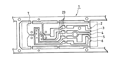
A metal stamping 1 as shown in Figs. 1 and 2 is
formed by blanking a metal plate in such a manner that it has
a first group of connector terminals 2, 3, 4, 5 and 6
arranged in cone of the two lines in which a number of
S connector terminals are arranged, and a wire pattern 7 to
which switches (described later) are connected. Those
connector terminals 2 through 6 are large current terminals.
A number of metal stampings may be formed one after another
by blanking a belt-shaped metal plate.
The metal stamping 1 is insert-molded by an insert
molding cavity for resin molding to obtain an insert molding
10 as shown in Fig. 3. Metal pieces 11 to 13 are each U-
shaped so as to have two legs, namely, a long leg and a short
leg. The metal pieces 11 to 13 are formed independently from
the metal stamping 1. The long legs of the metal pieces 11
to 13 serve as connector terminals 11', 12' and 13' arranged
in the other line, respectively. That is, the metal pieces
11 to 13 have the connector terminals 11' to 13' of a second
group, respectively. Those connector terminals 11' to 13'
are small current terminals, and are press-fitted in holes
14, 15 and 16, respectively, which are formed in the insert
molding 10. On the other hand, the short legs of the metal
pieces 11, 12, 13 are press-fitted in holes 17, 18 and 19,
respectively, which are formed in the insert molding 10, so
that they are electrically connected to the wiring pattern
and other circuit boards. In the embodiment, the short legs
- 6 -
~i821~~
are connected to a circuit board 20 (Fig. S) which is mounted
on the lower surface of the insert molding 10.
The terminals (long legs) 11', 12' and 13' of the
metal pieces 11, 12 and 13, which are press-fitted in the
holes 14, 15 and 16, respectively, are extended through parts
a, b and c (Fig. 2) of the metal stamping 1. The short legs
of the metal pieces 11, 12 and 13, which are press-fitted in
the holes 17, 18 and 19, respectively, are extended through
parts d, a and f (Fig. 2) of the metal stamping 1. As shown
in Fig. 3, a tubular wall 21 is extended from the lower
surface of the insert molding 10 in such a manner that it
surround the connector terminal section. A switch mounting
area is provided in the upper surface of the insert molding
10. In addition, the insert molding 10 has a plurality of
holes 23a which are formed by removal of the portions 23
(Fig. 1) of the metal stamping during insert molding. The
terminals 2, 3, 4, 5 and 6 in the one line (or the large
current terminals 2 through 6) and the terminals 11', 12' and
13' in the other line (or the small current terminals) are
arranged as shown in Fig. 4. Those connector terminals 2 to
5, and 11' to 13' are the male terminals through which a
plurality of external loads are connected to switches adapted
to control those loads.
Fig. 5 is an exploded perspective view showing the
switch device 30 according to the invention, which is made up
of the above-described insert molding 10 and circuit board
z~~z~~
20. The switch device 30, as shown in Fig. 5, is constituted
by a casing 31 in which the insert molding 10 is built; a
cover 32 which covers the bottom of the casing 31; and
operating knobs 33 and 34 which appear in the upper surface
of the casing 31 and are used to operate a movable plate 35
and switch 36 (described later), respectively. The switches
35 and 36 are arranged on the insert molding 10 and the
circuit board 20, respectively. The movable plate 35 is
engaged with a plunger 38 assembled to the knob 33. An
operating pieces 361 of the switch 26 is engaged with an
operating stem 39 extended downwardly from the operating knob
34. The terminals of the switch 36 are electrically
connected to a circuit pattern printed on the rear surface of
the circuit board 20. In the embodiment, the terminals of
the switch 35, which is operated with the operating knob 33,
correspond to terminals 2, 3, 4, 5 and 6; while the terminals
of the switch 36, which is operated with the operating knob
34, corresponds to the terminals 11', 12' and 13'.
The operating knobs 33 and 34 are swingably mounted
on the casing 31 through shafts which are extended
perpendicular to the longitudinal direction (or the front-to-
rear direction) of the casing. Each of the knobs 33 and 34
has a so-called "click mechanism" with which, when the knob
is swung in a direction to some extent, it is caused to
automatically swing in that direction. As the operating
knobs 33 and 34 are turned, the switches 35 and 36 are turned
_ g _
21$144
on and off, and the "on" and "off" signals of those switches
are transmitted through the connector terminals to control
circuits (not shown) such as for instance an electric motor
control circuit. In the embodiment, the operating knob 33 is
for a power window; that is, it actuates an electric motor to
open and close a window of a motor vehicle. The operating
knob 33 is to turn on and off a door locking mechanism of the
motor vehicle. The cover 32 together with the insert molding
and the circuit board 20 is secured to the casing 31 with
10 screws 37. The casing 31 is mounted in a recess formed in
the arm rest of a door of a motor vehicle in such a manner
that the top of the casing 31 is exposed. The connector
terminals exposed below the casing 31 (which are surrounding
by the tubular wall 21) are engaged with female terminals
(not shown) which are connected through a cable to external
loads.
Fig. 6 is an electrical circuit diagram of the switch
device 30 shown in Fig. 5. The switch 35 is connected to a
power circuit provided for an electric motor M which is
adapted to open and close a window of a motor vehicle, and
the switch 36 is connected to a power circuit provided for a
door locking mechanism of the motor vehicle, to control the
operation of the door locking mechanism.
Second Embodiment
Fig. 7 is an exploded perspective view showing the
arrangement of the switch device according to a second
_ g _
2182144
embodiment of the invention. The switch device 40 has no
operating knob for the door locking mechanism, and has only
one operating knob 33 to control the power window. In the
second embodiment, its insert molding 10 is the same as the
above-described one, and has the terminals 2, 3, 4, 5 and 6
of the metal stamping. However, in the second embodiment,
unlike the first embodiment, it is unnecessary for the insert
molding 10 to have the connector terminals (or small current
terminals) 11', 12' and 13' of the metal pieces 11, 12 and
13. That is, the second embodiment and the first embodiment
employ the same inserting molding, but are different from
each other in the purpose of use (or in the type of
operation). In other words, the second embodiment has no
door-locking-mechanism operating knob, and accordingly it is
unnecessary to press-fit the metal pieces 11, 12 and 13 into
the insert molding 10.
As was described above, in the embodiments of the
invention, the connector terminals 2 to 6 of the metal
stamping 1 are subjected to insert molding to form the insert
molding 10, and the remaining terminals 11' to 13' are press-
fitted in the insert molding 10. Accordingly, the connector
terminals arranged in plural lines are provided. This
feature makes it possible to simplify the stamping metal mold
and the insert-molding and accordingly to reduce the
manufacturing cost of the switch assembly. And even a switch
device in which it is unnecessary to arrange connector
- 10 -
2~ ~~~f ~~
terminals in plural lines, can employ the same insert molding
although, in this case, the metal pieces 11, 12 and 13 are
not press-fitted therein.
While there has been described in connection with the
5 preferred embodiments of the invention, it will be obvious to
those skilled in the art that various changes and
modifications may be made therein without departing from the
invention. For instance, in the above-described embodiments,
the connector terminals are exposed below the casing 31;
10 however, the technical concept of the invention is applicable
to a switch device in which its terminals are protruded from
the sides of the switch device, or from the front and the
rear.
According to the present invention, among the
connector terminals arranged in plural lines, the first group
of connector terminals in one line are parts of the metal
stamping, and the second group of connector terminals in
another line are parts of the metal pieces different from the
metal stamping. Hence, in the switch device of the
invention, when compared with a switch device in which
connector terminals arranged in plural lines are parts of one
metal stamping, the manufacture of its metal stamping is less
in the number of bending steps, and is less in the number of
wasteful portions. Furthermore, the metal stamping can be
formed with a simple stamping metal mold. And even in the
case where there are two kinds of switch devices - a first
- 11 -
switch device in which connector terminals arranged in one
line, and a second switch device in which connector terminals
arranged in two lines, the insert molding can be commonly
applied to those switches, which contributes to a reduction
in the manufacturing cost of the switch device.
In addition to the above-described effects, as for a
switch which needs not employ the small current terminals, it
is unnecessary to press-fit the small current terminals in
the insert molding, and therefore the insert molding can be
used commonly for two kinds of switches - one needs the small
current terminal, and the other needs not.
In addition to the above-described effect, in the
switch device, the insert molding is simplified in
construction, and it can be formed with a simple insert-
molding metal mold. This means that the molding cycle is
shortened, and the switch device is reduced in manufacturing
cost as much.
Furthermore, the switch device may be employed as a
power window switch having a plurality of operating knobs
which is simple in construction and small in size. This
feature results in a great reduction in the manufacturing
cost of the switch device.
- 12 -