Note: Descriptions are shown in the official language in which they were submitted.
2188358
TITLE OF THE INVENTION:
Optical Modulation System
NAME(S) OF INVENTOR(S):
Michael J. Sieben
Jan Conradi
David E. Dodds
FIELD OF THE INVENTION
This invention relates to fiber optic
communication systems and to the generation of optical
vestigial sideband signals, more particularly, for the
purpose of transmitting digital information.
BACKGROUND OF THE INVENTION
The single most fundamental limitation to the
signal bandwidth that can be transmitted on optical fibers
is chromatic dispersion of the modulated signal in the
fiber. In essence, an amplitude modulated optical signal
will usually have two information sidebands, one above and
the other below the optical frequency of the original light
source. The frequencies associated with these sidebands
will travel down an optical fiber at different velocities
with the result that different parts of the spectrum will
arrive at the far end at different times. Thus, if digital
signals are sent as narrow pulses, these pulses will be
broadened or dispersed, eventually overlapping with
neighbouring pulses.
Approaches currently used to reduce the effects
of chromatic dispersion include (1) reversing the effects
of chromatic dispersion in the optical domain, (2)
reversing the effects in the electrical domain and (3)
21'~8'3~8
reducing the transmission bandwidth of the optical signal
on the fiber. The first is based on purely optical methods
where the effects of group velocity dispersion are reversed
while the signal is still in the optical domain. Adding
dispersion compensating fiber in the transmission path is
a common approach. Other optical methods include
compensation by differential time delay of the upper and
lower sidebands of the modulated signal, see A.
Djupsjobacka, O. Sahlen, "Dispersion compensation by
differential time delay," IEEE Journal of Lightwave
Technology, vol. 12, no. 10, pp. 1849-1853, Oct. 1994;
spectrally inverting the signal at the midpoint of the
transmission path, see R.M. Jopson, A.H. Gnauck, R.M.
Derosier, "10 Gb/s 360-km transmission over normal-
dispersion fiber using mid-system spectral inversion,"
Proceedings OFC'93, paper PD3, 1993; and prechirping the
transmitted signal in an external modulator, see F. Koyoma,
K. Iga, "Frequency chirping in external modulators,"IEEE
Journal of Lightwave Technology, vol. 6, no. 1, pp. 87-93,
Jan. 1988 and A.H. Gnauck, S.K. Korotky, J.J. Veselka, J.
Nagel, C.T. Kemmerer, W.J. Minford, D.T. Moser, "Dispersion
penalty reduction using an optical modulator with
adjustable chirp," IEEE Photonics Technology Letters, vol.
3, no. 10, pp. 916-918, Oct. 1991.
The second approach, in which dispersion effects
are reversed in the electrical domain, is based on coherent
transmission and heterodyne detection followed by
equalization in the electrical domain. It is important to
note that a double sideband (DSB) signal must be heterodyne
detected if the signal is to be compensated electrically.
If homodyne detection were attempted with a DSB signal, the
upper and lower sidebands would overlap upon detection and
the phase information would be lost and the higher
modulation frequencies severely attenuated or distorted
~188~
through cancellation of sideband components. Some
techniques used or proposed for post-detection equalization
include microstrip lines, see K. Iwashita, N. Takachio,
"Chromatic dispersion compensation in coherent optical
communications," Journal of Lightwave Technology, vol. 8,
no. 3, pp. 367-375, Mar. 1990; microwave waveguides, see
J.H. Winters, "Equalization in coherent lightwave systems
using microwave waveguides," Journal of Lightwave
Technology, vol. 7, no. 5, pp. 813-815, May 1989.]
and fractionally spaced equalizers, see J.H. Winters,
"Equalization in coherent lightwave systems using a
fractionally spaced equalizer," Journal of Lightwave
Technology, vol. 8, no. 10, pp. 1487-1491, Oct. 1990.
The third approach is to modify the transmission
format where the baseband signal spectrum is compressed.
These types of approaches, which reduce the transmission
bandwidth required on the fiber to transmit a given bit
rate, are generally implemented by modifying the line code
format in order to reduce the effective bandwidth required
to transmit or receive the data, see K. Yonenaga, S.
Kuwano, S. Norimatsu, N. Shibata, "Optical duobinary
transmission system with no receiver sensitivity
degradation," Electronics Letters, vol. 31, no. 4, pp. 302-
304, Feb. 1995, and G. May, A. Solheim, J. Conradi,
"Extended 10 Gb/s fiber transmission distance at 1538nm
using a duobinary receiver," IEEE Photonics Technology
Letters, vol. 6, no. 5, pp. 648-650, May 1994.
The generation, transmission and detection of
single sideband (SSB) signals has been used in the RF and
microwave regions of the electromagnetic spectrum to reduce
the bandwidth of the signal by a factor of two, by sending
either the upper or the lower sideband. Generation and
transmission of SSB optical ~ignals using a Mach-Zehnder
modulator is shown in M. Izutsu, S. Shikama, T. Sueta,
21~3S8
"Integrated optical SSB modulator/frequency shifter," IEEE
Journal of Quantum Electronics, vol. QE-17, no. 11, pp.
2225-2227, Nov. 1981 and R. Olshansky, "Single sideband
optical modulator for lightwave systems," U.S. Patent No.
5,301,058, 1994. A dispersion benefit accrues from a single
sideband signal due to the fact that the transmitted signal
spectrum has been reduced by a factor of two.
A more significant advantage of optical SSB
transmission is that upon detection, particularly if the
signal is coherently detected, a dispersed baseband signal
is produced where the information of the relative arrival
time of the various signal frequencies remains as part of
the electrical output signal and hence the fiber dispersion
can be compensated in the electrical domain after
detection. This advantage is similar to that for
heterodyne detection of DSB signals, but with SSB
transmission and detection, the signal can be homodyned
directly to baseband using carrier signal added either at
the source or at the receiver and thus it can be directly
detected with the phase or delay information of the
transmitted signal preserved.
An early integrated optical SSB modulator using
optical filtering techniques was described in K. Yonenaga,
N. Takachio, "A Fiber chromatic dispersion compensation
technique with an optical SSB transmission in optical
homodyne detection systems," IEEE Photonics Technology
Letters, vol. 5, no. 8, pp 949-951, Aug. 1993, where
integrated optical structures were used to generate single
sideband tones for narrowband applications. In K.
Yonenaga, N. Takachio, "Dispersion compensation for
homodyne detection systems using a 10 Gb/s optical PSK-VSB
signal," IEEE Photonics Technology Letters, vol. 7, no. 8,
pp. 929-931, Aug. 1995, a single sideband optical modulator
was described for the purpose of transmitting two or more
~!18~ba~; 8
optical signals with different optical carrier frequencies
on a single fiber. The purpose of transmitting the signals
in a single sideband format is to permit these optical
carrier frequencies to be spaced as closely as the m~;mum
modulation frequency. In one of the variations described
in Yonenaga et al 1995, each optical SSB signal was
generated with a single Mach-Zehnder (MZ) modulator. The
input electrical information was modulated on RF sine and
cosine carriers for the purpose of driving each arm of the
dual-arm drive MZ modulator. By modulating the input
signals on RF carriers, the application can be classified
as a narrowband one since the bandwidth of the information
signal carried by each RF carrier is small compared to the
RF carrier frequency. When an information signal is used
to narrowband modulate a sinewave carrier, the Hilbert
transform of this modulated sinewave carrier is equivalent
to a cosine carrier modulated by the original information
signal. Further work on generation of SSB optical signals
with a Mach-Zehnder modulator is found in Olshansky, United
States patent no. 5,301,058.
SUMMARY OF THE INVENTION
The primary purpose for transmitting digital
signals in optical SSB or VSB format is to combat the
effects of chromatic dispersion encountered by the signal
as it propagates through an optical fiber.
An optical VSB system can provide close to the
same benefits of an optical SSB system since only the phase
information of those low modulation frequencies within the
vestigial spectrum are not preserved upon self-homodyne
detection. Low modulation frequencies are represented in
the vestige of the optical sideband which has otherwise
been mo8tly removed. This results in only a very small
dispersion impairment since low modulation frequencies are
~18~3~&
transmitted near the optical carrier frequency and thus
encounter very little difference in transmission velocity.
In the invention outlined here in its various
aspects, methods and apparatus are described that generate
broadband VSB digital signals in an optical form that does
not require the use of a specially constructed optical
filter and that permit the use of self-homodyne detection
of the transmitted light. The invention provides for an
improvement in performance relative to conventional double
sideband transmission due to a combination of both
bandwidth reduction and phase preservation.
Optical transmitters are described that generate
optical vestigial sideband (VSB) signals. The description
assumes an information source of data in a baseband format
which might be in the order of 2.5 - 100 Gb/s. In all of
the designs, the Hilbert transform or an approximation of
a Hilbert transform of a baseband input signal is derived.
Hilbert transforming a signal is a process which shifts by
90 degrees all frequency components of that signal without
changing the amplitude of those components. In all of the
designs, both the input signal and the Hilbert transform
signal are used to drive an optical modulator to create a
VSB signal. Two exemplary designs for the optical
transmitter are presented. In the first design, the
baseband signal and the Hilbert transform of that signal
each drive one arm of a modulator, preferably a dual arm
drive Mach-Zehnder (MZ) modulator. The Hilbert transform is
created using a tapped delay element. A dc bias is added to
one or both arms of the modulator in order to create an
optical phase difference of 90 degrees between the optical
carrier in each arm of the modulator. In this design, an
additional unmodulated optical carrier with the appropriate
phase i8 added to the transmitted 6ignal in order to
properly self-homodyne detect the optical signal. The
~ i 8~;~53
appropriate phase of the added carrier is such that the
resultant total output of the modulator is amplitude
modulated by the baseband signal and phase modulated by the
Hilbert transform of the baseband signal.
In the second design, a combination of the
baseband signal and the Hilbert transform of that signal
drive one arm and a different combination of the baseband
signal and the Hilbert transform signal drive a second arm
of a carrier optical signal modulator, for example a dual
arm drive MZ modulator. The combination of the baseband
signal and its transform are selected so that the amplitude
of the carrier optical signal is affected primarily by the
baseband signal, and less so by the Hilbert transform. A
dc bias is added to one or both arms of the modulator in
order to create a phase difference of 90 degrees between
the optical carrier in each arm of the modulator. In this
design, additional unmodulated optical carrier does not
have to be added to the transmitted signal in order to
properly self-homodyne detect the optical signal since the
modulation technique used guarantees that some optical
carrier will be transmitted.
There are three designs or methods for generating
the Hilbert transform of the baseband signal. The first
two designs are based on successive mixing of the input
signal with a sinusoidal carrier and filtering of this
mixed signal to generate the Hilbert transform of the input
signal. The third design generates the Hilbert transform
of the input signal by weighting and summing delayed
versions of the input signal. Several structures, referred
to in this patent documents as tapped delay elements, can
perform the functions of weighting and summing the delayed
versions of the input signal.
The present invention allows ~elf-homodyne
detection at the receiver by using the widely adopted
~18~5~
square law optical detector. Transmitting an optical VSB
signal over fiber will result in reduced effects of
chromatic dispersion as compared to transmitting in a DSB
format. This is due to bandwidth reduction. Furthermore,
the use of VSB instead of DSB allows most of the received
signal to be delay equalized upon detection which can
largely reverse the effects of chromatic dispersion.
BRIEF DESCRIPTION OF THE DRAWINGS
There will now be described preferred embodiments
of the invention, with reference to the drawings, by way of
illustration only and without intending to limit the scope
of the invention as claimed in the claims, in which like
numerals denote like elements and in which:
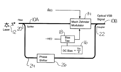
Fig. 1 is a schematic illustration of an optical
vestigial sideband transmitter that may be used with a
tapped delay element for generating a Hilbert transform
according to one aspect of the invention;
Figs. lA and lB are phasor diagrams showing phase
relationship of the signals of Fig. 1;
Fig. 2 iS a schematic illustration of an optical
vestigial sideband transmitter according to a second aspect
of the invention;
Figs. 2A and 2B are phasor diagrams showing phase
relationship of the signals of Fig. 2;
Fig. 3 is a schematic illustration of a dual arm
drive Mach Zehnder modulator;
Fig. 4 is a schematic illustration of a modified
version of Weaver's method for generating a signal and the
Hilbert transform of that signal;
Fig. 5 shows the signal spectra of an arbitrary
baseband signal at various stages of the design which
implements the modif ied Weaver approach ~o generate a
signal and the Hilbert transform of that signal;
~1~8~ 8
Fig. 6 is a schematic illustration of a second
modified version of Weaver's method for generating a signal
and the Hilbert transform of that signal;
Fig. 7 is a schematic illustration of a method
for generating two combinations of a signal and the Hilbert
transform of that signal;
Fig. 8 is a generalized schematic illustration of
a tapped delay method for generating an approximation of
the Hilbert transform of a signal;
Fig. 9 is a schematic illustration of a tapped
delay element system which provides a signal and the
approximate Hilbert transform of that signal;
Fig. 10 is a schematic illustration of a tapped
delay element system which provides two combinations of a
signal and the approximate Hilbert transform of that
signal; and
Fig. 11 is a schematic illustration of a receiver
system that detects the optical VSB signal and equalizes
the phase of the received electrical signal.
DETAILED DESCRIPTION OF PREFERRED EMBODIMENTS
An exemplary design for an optical transmitter to
be used with a Hilbert transform generator according to the
invention is shown in Fig. 1. A carrier optical signal is
coupled to an optical fiber 10A by laser 12. In this
design, baseband signal m(t) and the Hilbert transform m(t)
of that signal are each modulation signals that drive one
arm each of a dual arm drive Mach-Zehnder (MZ) modulator 14
connected between input optical fiber 10A and output
optical fiber 10B. A second exemplary design is shown in
Fig. 2. While the invention is described in relation to
optical signals carried by optical fibers, it will be
appreciated that the invention has application to any
optical signal transmitted along a suitable light guide. It
2~88~8
will further be appreciated that the Hilbert transform of
a signal cannot ever be exact, and if it is not exact then
to the extent of the inexactness, the modulation output
will not be a pure single sideband, but will have a
vestigial component.
A schematic of a dual arm drive MZ modulator is
shown in FIG. 3, including waveguide 32 embedded in a
substrate 33. Modulation signals vl(t) and v2(t) are applied
to electrodes 34 and 35 respectively to phase modulate the
optical carrier signal passing along the waveguides 32a and
32b respectively. The electromagnetic field established
between the electrode 34 and the ground 36 and between
electrode 35 and the ground 36 alters the index of
refraction of the waveguide to phase modulate the
electrical signals onto the optical signal.
As shown in fig. 1, a dc bias equivalent to
V~/2, where Vn is the modulator's switching voltage, is
added from bias source 16 to the Hilbert transform signal
at bias Tee 18 in order to create a phase difference of 90
degrees between the light in each arm of the modulator.
The absolute dc bias added to each arm can be varied but
the relative difference between the dc bias values in each
arm should be as close to V~/2 as can reasonably be
achieved. If a relative difference of -V~/2 were used, the
alternate Upper Sideband (USB) or Lower Sideband (LSB) is
transmitted depending on the polarity of m(t). Either the
USB or LSB is transmitted depending on both the phase
response of the fiber and that of any equalizer used at the
receiver to reverse the effects of the fiber phase
response.
In the embodiment shown in Fig. 1, additional
unmodulated optical carrier must be added to the
transmitted signal in order to properly self-homodyne
detect the optical signal. Means for accomplishing this
'~i883~ 8
includes a splitter 20 on the input optical fiber lOA
before the modulator 14, a coupler 22 on the output optical
fiber lOB after the modulator 14, and an optical fiber loop
24 connected between the splitter 20 and the coupler 22.
Delay on the optical fiber loop 24 represented by the phase
shifter should be such that carrier optical signal coupled
to the output optical fiber lOB is in the appropriate phase
relative to the modulated light output from the modulator
14. That is, the additional optical carrier when added to
the resultant optical signal from the modulator must
produce a total resultant optical signal which is amplitude
modulated primarily by m(t) and phase modulated primarily
by m(t)-
The phase relation of the optical signals in the15 upper arm and the lower arm of a dual arm Mach-Zehnder (MZ)
modulator are shown in the phasor diagram of Fig. lA. The
phase of the optical signal in the upper arm is modulated
by m(t) and the phase of the optical signal in the lower
arm is modulated by -m(t). The upper arm optical signal and
the lower arm optical signal are added at the MZ output to
form the modulator resultant optical signal S. The ellipse
E1 in Fig. lB represents the possible positions of the
resultant S, as m(t) and m(t) vary with time. The phase
relations of the added carrier, C, the modulator resultant,
S, and the total resultant signal T are illustrated in Fig.
lB. The total resultant T is in phase with the varation
caused by m(t), and the phase of the added carrier C is
adjusted in practice to ensure that this is approximately
the case. It will be observed that, with proper added
carrier phase, the amplitude changes of the total resultant
are primarily affected by only m(t), while m(t) has little
effect on the amplitude. It can be arranged that m(t) has
the primary effect on the amplitude of the resultant output
optical signal, but this is not preferred.
'~i883~
Self-homodyne detection is a method by which an
unmodulated carrier is included in the transmitted signal
such that upon square law detection the unmodulated carrier
acts as a local oscillator at the receiver so that the
information signal is properly mixed to baseband. The
power of this additional optical signal should be large
enough to properly self-homodyne detect the optical VSB
signal. It can be ensured that the added carrier has the
appropriate phase in relation to m(t) by varying the delay
of the added carrier by trial and error until the proper
phase is obtained.
An exemplary design for an optical transmitter
according to a second embodiment of the invention is shown
in FIG. 2, including the same optical fiber lOA, lOB and
modulator 14. In this embodiment of the invention, a
linear combination of the baseband signal m(t) and the
Hilbert transform m(t) of that signal drive one arm and a
different combination of the baseband signal and the
Hilbert transform signal drive a second arm of the dual arm
drive MZ modulator 14. The first combination signal may
consist of m(t) + m(t) (or an amplified version thereof)
while the second combination signal may consist of -m(t) +
m(t) (or an amplified version thereof). A dc bias is added
to one or both arms of the modulator 14 in order to create
a phase difference of about 90 degrees between the light in
each arm of the modulator 14. In the design shown in FIG.
2, the dc bias added at bias Tee 28 from bias source 29 to
the arm driven by m(t) +m(t) is equivalent to -V~/4 while
the dc bias added at bias Tee 30 from bias source 31 to the
arm driven by -m(t) + m(t) is equivalent to V~/4. Again,
the relative difference between the dc bias in each arm
should be V~/2 or -V~/2 depending on which sideband is to
be transmitted. In this design, additional unmodulated
optical carrier does not have to be added to the
2188358
transmitted signal in order to properly self-homodyne
detect the optical signal, since the output from the
modulator includes unmodulated optical carrier with the
appropriate signal phase. This combination of drive
signals allows the modulator to be driven such that the
phase modulation from m(t) is not detected by the square
law detector. That is, modulation of the carrier optical
signal by the baseband signal and its Hilbert transform
results in an output optical signal whose amplitude is
primarily affected by amplitude modulation due to the
amplitude of the baseband signal m(t). The optical signal,
however, remains VSB. Consequently, the design shown in
Fig. 2 presents an improvement over the design shown in
Fig.l in that extra unmodulated carrier does not have to be
added to the modulated light. Thus, with changes to the
electrical drive signals, existing modulator designs can be
used without optical modifications.
Various linear combinations of m(t) and m(t) may
be used providing they fulfill the following conditions:
(1) the output of the modulator has a single or
vestigial sideband;
(2) a part of the carrier optical signal passes
through the modulator; and
(3) the amplitude of the resultant output optical
signal is primarily affected only by one of the
signals m(t) and m(t), preferably m(t).
The phase relation of the optical signals in the
upper arm and the lower arm of a dual arm Mach-Zender (MZ)
modulator of Fig. 2 is illustrated in Fig. 2A. The phase
of the optical signal in the upper arm is modulated by m(t)
+ m(t) and the phase of the optical signal in the lower arm
is modulated by -m(t) + m(t). The upper arm optical signal
and the lower arm optical 6ignal are added at the MZ output
to form the modulator resultant optical signal R. The
~lg835~
14
ellipse E2 in Fig. 2B represents the possible positions of
the resultant, R, as m~t) and m(t) vary with time. It is
thus seen that the amplitude (length) of R is primarily
affected by the signal m(t) and m(t) does not significantly
affect the amplitude of R. Hence, the signal m(t) can be
recovered from the amplitude variation of R. This
combination of m(t) and m(t) for the MZ drive signals
allows for larger optical signal modulation with less
distortion than the method of Olshansky.
In a first design to generate the Hilbert
transform of a baseband signal, a modified version of
Weaver's approach is used as shown in FIE. 4. A method of
generating an electrical SSB signal was originally
disclosed by Weaver 1956. In this modified approach the
carrier frequency, fb, used in the various product
modulators is equal to the frequency at which the first
null in the power spectral density of the input baseband
data signal occurs. For binary data signals, this frequency
is at the bit rate, for multi-level signals this frequency
is at the baud rate.
The input signal m~(t) at (i) in FIG 4 is first
bandlimited by filter 40 and, for binary data signals, this
is usually limited to frequencies less than fb. In FIG. 4,
the bandlimited signal at point (ii) is passed to product
modulator 41 where it amplitude modulates, in double
sideband form, a cosine carrier whose frequency is equal to
bit rate fb to form the signal at point (iii). This is
filtered in high pass filter 42 to leave the upper sideband
at point (iv). It is possible to use a lowpass filter in
place of the highpass prefilter; however, there is an
implementation advantage to a highpass or a bandpass design
at frequencies above 10 GHz. Furthermore, the highpass
filter results in a larger gap between wanted and unwanted
21g8~8
frequencies at points (v) and (vi) and this reduces the
required complexity of the lowpass filters which follow.
Output from the high pass filter 42 is passed to
product modulator 43 where it modulates the same carrier
signal as at product modulator 42. Product modulation
output from this product modulator 42 is low pass filtered
at filter 44 and amplified using amplifier 45 as required
to yield m(t). Output from the high pass filter 42 is also
passed to product modulator 46 where it modulates the same
carrier signal as at product modulator 42 but where the
carrier has been shifted in phase by 90~. Thus, if the
carrier at 41 is a cosine carrier, the carrier at 46 is a
sine carrier, and vice versa. Product modulation output
from this product modulator 46 is low pass filtered at
filter 47 and amplified using amplifier 48 as required to
yield m(t). The first inphase modulator and filter has
output m(t) at point (ix) which is substantially the same
as the input signal. The first quadrature modulator and
filter has output m(t) at point (x) which is the Hilbert
transform of m(t). The magnitude spectrum of m(t) is the
same as m(t) but the phase spectrum is different. The
modulation system shown in Fig. 4 has the capability of
handling DC signals, but the filter 42 must be carefully
designed with 50% gain at fb and symmetric about the
center.
The spectra of the signals at various stages in
the system using the Hilbert transform generator shown in
FIG. 4 are shown in FIG 5. An arbitrary binary baseband
signal is chosen for illustrative purposes. FIG. 5(a)
represents the original baseband signal while FIG. 5(b)
represents the lowpass filtered version of FIG. 5(a). FIG.
5(c) represents the spectrum after the modulation by the
first carrier and FIG. 5(d) represents the highpass
filtered version of FIG. 5(c). FIG. 5(e) represents the
2i883~8
16
signal after the second mixing and FIG. 5(f) the lowpass
filtered version of FIG. 5(e). The output of the optical
transmitter which results in a optical VSB signal is shown
in FIG. 5(g). At the receiver, self-homodyne detection by
a square law optical detector results in the recovered
baseband spectrum shown in FIG. 5(h).
In contrast to Weaver~s method, the design
disclosed here uses lowpass filters and first quadrature
modulators operating at fb equal to B, the bandwidth
required to transmit the information signal, as opposed to
0.5B as Weaver does. Further, the method disclosed here
does not require oscillation frequencies other than fb
equal to the baud rate B for modulation or demodulation.
This frequency is readily available in any digital system.
Finally, the orientation of the final optical SSB spectrum
is correct such that self-homodyne detection results in the
proper receive baseband signal.
In FIG. 6, a modified version of the
implementation shown in FIG. 4 which generates the Hilbert
transform is shown. In FIG. 4, the signals at points (ii)
and (ix) are essentially the same so the redundant
components can be removed, leaving low pass filter 40,
product modulator 41, high pass filter 42, product
modulator 46, low pass filter 47 and amplifiers 45 and 48.
The original components are still required for the bottom
path in order to generate m(t). A delay 49 must be added in
the path generating m(t) to adjust its phase to the phase
of m(t)-
In order to generate the combination signals m(t)
+ m(t) and -m(t) + m(t), the designs shown in FIG. 4 and
FIG. 6 can be modified to include the design shown in FIG.
7. Signal m(t) is split at 70, amplified in amplifier 71,
inverted by inverting amplifier 72. The amplified signal is
fed to summer 73, and the inverted signal to summer 74. At
835g
the same time, signal m(t) is amplified in amplifier 75 and
fed to both summer 73 and 74 to yield a linear combination
of the signals m(t) and m(t).
In the third design to generate the Hilbert
S transform signal shown in Fig. 8, the Hilbert transforming
function is carried out by a tapped delay element 92. This
tapped delay approach to generating a Hilbert transform is
known in the art of generating Hilbert transforms in
itself. Tapped delay element 92 serves to take a time
derivative of the signal and apply a frequency dependent
weighting such that each frequency component has the same
amplitude before and after time differentiation. The
tapped delay Hilbert transform has zero output at 0 Hz
(DC). Thus for DC and very low frequencies, there is no
phase modulation of the optical output and thus the
transmitted optical spectrum is double sideband (DSB) for
very low frequencies. The total time delay through tapped
delay element 92 determines the lowest frequency which will
have equal amplitude at the input and the output while the
time delay T determines the highest frequency which can be
differentiated with respect to time. As shown in Fig. 9,
the signal m'(t) is first low pass filtered in low pass
filter 90 (Fig. 9) and then as shown in Fig. 8 passed along
bus 80 through delays 82 which have delay 2T between tap
lines 84 and have delay T on either side of the center tap
83. Tap lines 84, 83 connect to the bus 80 after each delay
82 and the tapped signals are weighted by weights 86 as
indicated in Fig. 8 and added in summer 88. The
configuration shown in FIG. 8 can be created with discrete
element splitters, delay lines and combiners or each entire
filter can be fabricated in microstrip form.
As shown in Fig. 8, the tapped delay element 92
is symmetrical, and has an impulse response defined by h(t)
= ~(n~ (t-n)T for n= -N to +N, where n is odd, 2T is the
~18835~
time delay between taps and 2N is the total number of taps
in the delay element.
In order to generate the proper signals for the
first optical modulator design, the design shown in FIG. 9
is used. The signal m(t) is simply time delayed by time
delay 94 in order to properly phase it with the Hilbert
signal m(t) and amplified as required in amplifier 96. In
FIG. 9, the Hilbert transform is shown as being created
from Tapped Delay Element 92 followed by amplifier 98.
Tapped Delay Element 92 should employ the tapped delay
element shown in FIG. 8 with coefficient a equal to 0. If
a filter with four taps were used as an example, a time
delay of 3T is required for m(t) in order to properly phase
it with the Hilbert signal m(t). The value of 2T is
generally less than one bit period for a digital signal.
For example, T is of the order of 40 ps for a 10 Gb/s
binary source.
In order to generate the proper signals for the
second embodiment of the optical modulator, the design
shown in FIG. 10 is used. The baseband signal m(t) is
first low pass filtered at filter 110 and passed to tapped
delay elements 112 and 114. Tapped Delay Element 112
employs the tapped delay element 92 shown in FIG. 8 with
coefficient a equal to 1 thus generating the signal m(t) +
m(t). Tapped Delay Element 114 employs the tapped delay
element shown in FIG. 8 with coefficient a equal to -1 thus
generating the signal -m(t) + m(t). Appropriate amplifiers
116 and 118 are used to condition the output from the
tapped delay elements 112 and 114.
All of the optical signals generated are
converted to electrical baseband signals in an optical
receiver using the general design shown in FIG. 11. The
output optical light guide lOB, typically an optical fiber
transmission line, forms part of a transmission system in
~21X~5g
19
which the output optical light guide lOB induces phase
distortion of transmitted signals. The received optical
signal is detected by a simple photodetector 120 employing
the common square-law detection operation. The subsequent
electrical signal is filtered by low pass filter 122 to
reduce noise power and equalized in electrical equalizer
124 to remove phase distortion induced by the optical light
guide lOB and restore the original phase of the information
signal m(t). The equalization can be performed with a
microstrip equalizer or other types of equalizers which
have the inverse phase characteristic of the fiber used for
transmission. Electrical amplifiers are added where
appropriate. Accordingly, this invention is capable of
modulating signals where the baseband digital broadband
signal m(t) includes a DC component, and the information in
the signal is coded by amplitude shift keying. It will be
appreciated that the Hilbert transform and the 90~ phase
differentials referred to in the claims are only
approximations, although severe departure from the
exactness of the Hilbert transform or from 90~ phase shifts
results in a degradation of performance.
A person skilled in the art could make immaterial
modifications to the invention described in this patent
document without departing from the essence of the
invention that is intended to be covered by the scope of
the claims that follow.