Note: Descriptions are shown in the official language in which they were submitted.
W O 96127836 PCTlUS96f03248
2189782
~~ ;;:~-~
SYSTEM AND METHOD FOR ERPANSION OF A COMPUTER
BACECGROUND
1. ~e Field Of the Tnvan+inn
This invention relates to digital computers. More
- specifically, the present invention relates to devices
used to expand the ability of an existing computer to
utilize additional hardware and provide additional
features for the user of the computer. -
2. The Prior Art
The widespread use of computers in industrial
societies has brought the benefits of computers to large
numbers of people. In particular, the standardization
and availability of personal computers has provided that
each user can customize such computers with a wide
variety of hardware and software. Unfortunately, some
users who want to add hardware to their computer find
that all available expansion slots or ports which can
accommodate such hardware have already been utilized in
their computer. Thus, the user must forego adding one
or more hardware items.
The problem of adding hardware is particularly -
troublesome to users of portable computers. Such
portable computers commonly are generally classified -
into laptop, note book, sub-note book, and palm top size
classes. The small size of these computers requires ---
that all of the components associated therewith be
mmiaturized_ In order to allow the user to add
hardware to such portable computers, an industry
standard promulgated by the Personal Computer Memory
Card International Association (PCMCIA) has gained wide -.
acceptance. Such hardware is commonly referred to as a
PC Card or a CardBus Card and is known as "PC Card
compliant," "PCMCIA compliant" or "CardBus compliant."
PC cards and CardBus Cards are compact hardware devices
having dimensions of about 2_1 inches by about 3.4
WO 96ff7836 PCTIU596103TA8
'. ( ~ C? f E
~~89782
2
inches with a thickness of only 3.Smm, Smm, 8mm or some
other dimensions allowed by the promulgated standard.
The PC Card typically slides into a socket provided on
the side of the portable computer to allow easy
replacement of one PC Card with another PC Card.
Increasingly, users of desktop computers, as well as
other electronic devices, are also using such cards to
add hardware devices to their computers.
Widely used hardware devices such as modems, random
access memory, and disk drives, for example, are all
available as PC cards and will soon be available as
CardBus Cards. There are, however, numerous hardware
devices which are not yet available, or which may never
be available, in a PC Card implementation or a CardBus
Card implementation. Thus, portable computer users are
unable to use the myriad of hardware devices which are
available to desktop computer users. Also, many
portable computers do not provide additional ports for
communication with hardware devices such as keyboards
and pointing devices. For the foregoing reasons,
portable computer users are unable to utilize many
hardware devices which are utilized by other computer
users. -
In order to provide computer users with additional
expansion capability and convenience of use for their
computers, devices referred to as "port replicators" and
"expansion chassis" have been provided. These devices
provide additional locations for other hardware devices
to interface with a computer. These other hardware
J
devices may-be stand alone, or external, devices which
are commonly configured to communicate with the computer
via a serial port using the widely known RS-232
communication protocol_ Alternatively, these other
hardware devices may be internal devices .which are
merely prihted circuit cards adapted to be installed
WO 96127836 PCT/U596103248
:q,~;-~:~,sr~ 2789782
3
inside the computer case and which comply with the
Industry Standard Architecture (ISA) standard or the
Peripheral Component Interconnect (PCI) standard. Port
replicators and expansion chassis can also be used to -
provide added convenience for a portable computer user -
by making connections to an external key board, external
video monitor, and the like, simpler than if each
external device needed to be connected to and
disconnected from the portable computer.
The previously available port replicators and
expansion chassis provide a few useful functions.
Disadvantageously, such devices cannot interface with a
PCMCIA socket provided in portable computers. Moreover, --
in many previously available port replicator devices and
expansion chassis, only particular types of expansion --
devices and/or expansion devices which comply with only
a less popular standard can be used. Alternatively,
some previously available port replicators and expansion
chassis utilize non-standard or proprietary connectors
and protocols which seriously limits their usefulness.
In view of the foregoing, it would be a significant
advance in the art to provide an improved system and
method for expanding a computer which overcomes the
drawbacks and disadvantages found in the previously
available devices.
BRIEF SUMMARY AND OBJ.rTS QF THE rNVENTTON
In view of the above described state of the art,
the present invention seeks to realize the following
objects and advantages.
It is a primary object of the present invention to
conveniently expand a computer using widely available
peripheral devices even though such devices are not'
intended to be used with the computer.
It is also an object of the present invention to
expand the capabilities of a portable computer, and
R'O 96127836 PCf/US96/03248
4
particularly a lap top or smaller- computer, using
devices intended to be installed in a desk top computer.
It is a further object of the present invention to
conveniently interface TSA compliant expansion add-on
printed circuit cards with a PCMCIA compliant socket.
It is a still further object of ahe present
invention to conveniently interface PCI compliant
expansion add-on printed circuit cards with a PCMCIA
compliant socket.
It is yet another object of the present invention
to conveniently interface both ISA compliant expansion
add-on printed circuit cards and PCI compliant expansion
add-on printed circuit cards with a PCMCIA compliant
socket using a single device.
It is another object of the present invention to
conveniently interface ISA or PCI compliant devices with
a PCMCIA compliant socket without requiting modification
of the software used with the ISA or PCI compliant
devices.
It is-also an object ofthe present invention to
expand the number of ISA ports and/or PCI ports found on
a lap top or smaller computer via the PCMCIA socket
present on the computer.
It is yet another object of the present invention
to interface a device which requires any one of a number
of different interrupt requests with a computing device
which provides only one interrupt request_
It is--a further object of the present invention to
interface a device which requires direct memory access
with a computing device which does not provide direct
memory access.
It is still another object of the present invention
to accurately translate the timing of ISA compliant
signals and/or PCI compliant signals to PCMCIA compliant
signals and to accurately translate PCMCIA compliant
WO 96127836 PCTIU596103248
- ' ; '~ 189782
w~~;':~ -~~' 2
signals to ISA compliant signals and/or PCI compliant
signals in a manner which is transparent to the devices
involved and to the user of the computer.
It is also an object of the present invention to
interface 8 bit memory peripheral devices with a
computing device which only accommodates 16 bit memory
device signals.
It is yet another object of the present invention
to supply the voltage and current requirements of an ISA
compliant add-on expansion printed circuit card and/or
a PCI compliant add-on expansion printed circuit card
which cannot be supplied by the host computer.
These and other objects and advantages of the -
invention will become -more fully apparent from the
description and claims which follow, or may be learned
by the practice ofthe invention.
The present invention provides a system and method
for interfacing at leastone ISA compliant device or at -
least one PCI compliant device with a PCMCIA compliant
socket on a host computer. The present invention is -
particularly useful to allow ISA compliant devices or at
least one PCI compliant device, which could not
otherwise be used with a portable computer, to be used -
with such computers.
The present invention advantageously can provide -
complete compatibility between a PCMCIA socket and ISA -
compliant devices -and/or PCI compliant devices,- even
though the PCMCIA industry standard is very different
and includes contradictory requirements than the ISA and
the PCI standards. Thus, with the present invention,
any numberof different ISA compliant devices and/or PCI
compliant devices can be interfaced with the PCMCIA
socket of a host computer. This allows a user to easily
connect and disconnect numerous ISA compliant devices
and/or PCI compliant devices via a single PCMCIA socket
CA 02189782 2001-02-21
78030-1
6
commonly found on portable computers and also on desk top
computers. The embodiments of the present invention preferably
provide all of the functions necessary to interface a PCMCIA
compliant socket with nearly all available ISA and/or PCI
compliant devices.
In accordance with the present invention, there is
provided a system for providing translation between a host
computer having a first port, the first port compliant with a
first standard, and a hardware device which is compliant with a
second standard, the first standard and the second standard
being non-compatible with each other, the system comprising:
means for direct memory access translation between the host
computer and the hardware device; means for supplying power to
the hardware device; and means for translating the timing
between the host computer and the hardware device such that the
host computer and the hardware device are interfaced and the
functions of the hardware device are provided to the host
computer.
In accordance with the present invention there is
further provided a system for providing translation between a
host computer having a first port, the first port compliant
with a first standard, and a hardware device which is compliant
with a second standard, the first standard and the second
standard being non-compatible with each other and the hardware
device requiring support for a plurality of interrupts, the
system comprising: means for interrupt translation between the
host computer and the hardware device; means for supplying
power to the hardware device; and means for translating the
timing between the host computer and the hardware device such
that the host computer and the hardware device are interfaced
and the functions of the hardware device are provided to the
host computer.
CA 02189782 2001-02-21
78030-1
7
In accordance with the present invention there is
further provided a system for expanding a host computer having
a PCMCIA compliant port and allowing the host computer to
interface with at least one ISA compliant device, the system
comprising: means for making electrical and physical connection
to the PCMCIA compliant port; means for making electrical
connection to the at least one ISA compliant device; means for
interrupt translation between the PCMCIA port and the at least
one ISA compliant device; means for direct memory access
translation between the PCMCIA port and the at least one ISA
compliant device; means for providing a clock signal to the ISA
compliant device; means for supplying power to the at least one
ISA compliant device; and means for translating the timing
between the PCMCIA port and the ISA compliant device such that
the host computer can utilize the functions of the at least one
ISA compliant device.
In accordance with the present invention there is
further provided a method for providing translation between a
host computer having a first port, the first port compliant
with a first standard, and a hardware device which is compliant
with a second standard, the first standard and the second
standard being non-compatible with each other and the hardware
device requiring support for a plurality of interrupts, the
method comprising the steps of: translating between the
interrupts of the host computer and the interrupts of the
hardware device; supplying power to the hardware device; and
translating the timing between the host computer and the
hardware device such that the host computer and the hardware
device are interfaced and the functions of the hardware device
are provided to the host computer.
In accordance with the present invention there is
further provided a method for providing translation between a
host computer having a first port, the first port compliant
CA 02189782 2001-02-21
78030-1
, 8
with a first standard, and a hardware device which is compliant
with a second standard, the first standard and the second
standard being non-compatible with each other, the method
comprising the steps of: direct memory access translation
between the host computer and the hardware device; supplying
power to the hardware device; and translating the timing
between the host computer and the hardware device such that the
host computer and the hardware device are interfaced and the
functions of the hardware device are provided to the host
computer.
In accordance with the present invention there is
further provided a method for expanding a host computer having
a PCMCIA compliant port and allowing the host computer to
interface with at least one ISA compliant device, the method
comprising the steps of: making electrical and physical
connection to the PCMCIA compliant port; making electrical
connection to the at least one ISA compliant device;
translation between the PCMCIA port interrupt and the
interrupts of the at least one ISA compliant device; direct
memory access translation between the PCMCIA port and the at
least one ISA compliant device; providing a clock signal to the
ISA compliant device; supplying power to the at least one ISA
compliant device; and translating the timing between the PCMCIA
port and the ISA compliant device such that the host computer
can utilize the functions of the at least one ISA compliant
device.
BRIEF DESCRIPTION OF THE DRAWINGS
In order to better appreciate how the above-recited
and other advantages and objects of the invention are obtained,
a more particular description of the invention briefly
described above will be rendered by reference to a specific
embodiment thereof which is illustrated in the appended
CA 02189782 2001-02-21
78030-1
, 9
drawings. Understanding that these drawings depict only a
typical embodiment of the invention and are not therefore to be
considered limiting of its scope, the invention will be
described and explained with additional specificity and detail
through the use of the accompanying drawings in which:
Figures lA and 1B are perspective external views of a
first presently preferred embodiment of the present invention.
Figure 2 is a perspective internal view of the first
presently preferred embodiment represented in Figures lA-B.
Figure 3 is a block diagram showing the principal
functional components included in one representative preferred
embodiment of the invention.
Figure 3A is a block diagram showing the principal
functional tasks carried out by the translator circuit
represented in Figure 3.
Figures 4A-B are flow charts showing the pertinent
steps carried out by the embodiment of the invention.
Figures 5A-L are timing diagrams showing the timing
operations of the components represented in Figure 3.
DETAILED DESCRIPTION OF THE PREFERRED EMBODIMENTS
Reference will now be made to the drawings wherein
like structures will be provided with like reference
designations. Figures lA and 1B are perspective external views
(not necessarily to scale) of a first presently preferred
embodiment of the present invention. The embodiment
illustrated herein will be used as one example of the inventive
concepts of the present invention with the understanding that
many other particular renderings of the present invention are
CA 02189782 2001-02-21
78030-1
9a
also possible and can be arrived at by those skilled in the art
using the teachings presented herein.
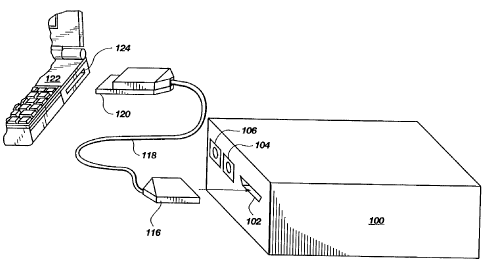
Represented in Figures lA-B is a host computer 122
having a PCMCIA compliant socket 124. The Personal Computer
Memory Card International Association (PCMCIA) promulgates the
PCMCIA standard which has gained wide acceptance in the
industry. It is preferred that the PCMCIA compliant socket
adhere to PCMCIA release 2.1 specification, Type II extended
card standard. This preferred standard specifies the physical,
electrical and environmental parameters which compliant devices
must meet. The system and method of the present invention
described herein are compatible with the PCMCIA Card Services
Specification 2.1 and Card Services Specification 2.1 as well.
This standard and the accompanying specifications are well-
known in the art and the subject matter of PCMCIA release 2.1,
PCMCIA Card Services Specification 2.1, and Card Services
Specification 2.1, PCMCIA Standard Release 2.1, and all
releases promulgated thereafter (including the PC Card standard
(1995)). It is to be understood that the present invention can
be utilized with other PCMCIA specifications and standards
which are now available or which become available in the future
as well as with other similarly instructive standards which are
now available in the industry or which become available in the
future. Examples of such other specifications and standards
include the CardBus PC Card standard. Further information
regarding the implementation of these standards can be obtained
from the publication Anderson, D. & Shanley, T., CARDBUS SYSTEM
ARCHITECTURE (1996)(published by Addison-Wesley Publishing
Company).
In its most advantageous use, the embodiment of the
present invention described herein allows ISA and/or PCI
compliant devices to interface with the PCMCIA socket of a
portable computer and allow the portable computer to access all
CA 02189782 2001-02-21
78030-1
, 9b
of the functions of the ISA or PCI compliant device. As is
known in the art, ISA and PCI compliant devices are widely
available in the industry. Many ISA and PCI compliant devices
are configured as "add-on cards" which are printed circuit
boards provided with an edge connector which is received into
an open slot coupled to the back plane of a desktop computer.
The "add-on cards" are often as large as the portable host
computer 122 with which the apparatus of the present invention
is used. While the described embodiment of the present
invention is explained herein for use with a portable computer,
the present invention can also advantageously be used with
other computing devices.
The present invention provides that the wide variety
of devices available as add-on cards at a reasonable cost can
be conveniently used with all portable computers having a
PCMCIA socket. Moreover, as will be explained more fully later
in this disclosure, the embodiments of the present invention
also allow a portable computer user to connect and disconnect a
full size keyboard, a pointing device (such as a mouse), a
video add-on card, a video monitor, and other ISA compatible
devices (which would generally be used only with a desktop
computer) by merely inserting and removing a single plug into
the PCMCIA socket in the portable computer. Moreover, the
present invention is more flexible, and less costly, than
providing a proprietary docking station for a portable computer
which only provides, for example, an independent key board and
another device which is not ISA compliant or PCI compliant.
It is understood in the industry that the ISA
standard for PC compatible computers has not been promulgated
by a single entity but has evolved through the years based upon
the original architecture of the IBM PC Personal Computer.
Nevertheless, the ISA standard is well-known in the industry.
Information regarding the ISA standard is contained in the
CA 02189782 2001-02-21
78030-1
, 9c
publications: Solari, Edward, ISA & EISA THEORY AND OPERATION
(Annabooks publication); Shanley, Tom & Anderson, Dan, ISA
SYSTEM ARCHITECTURE and Messmer, Hans-Peter, THE INDISPENSABLE
PC HARDWARE BOOK. The PCI standard was developed by Intel
Corporation and is managed by a consortium of industry partners
known as the PCI Special Interest Group. Revision 2.1 of the
specification for the CardBus standard is available for PCI
Special Interest Group. Further information regarding the PCI
standard can be obtained from the publication Anderson, D. &
Shanley, T., PCI SYSTEM ARCHITECTURE (1995)(published by
Addison-Wesley Publishing Company).
R'O 96127836 PCfIUS961D3248
~; i ,~
. " :"~.~ r ~. : a .
,~ X189782
~ ' ~~( w °r-' :~j Ie
' ~~ 1 f. ~ : _
The embodiment of the present invention described
herein provides includes a translation driver which is
loaded onto the portable computer 122, preferably as
software, which allows the portable computer to
S interface-.with ISA and/or PCI compliant devices in a
transparent manner, that is, without modification of the
other functions of the portable computer and without the
user taking any notice .- during operation.
Advantageously, any ISA and/or PCI device drivers which
10 accompany the ISA and/or PCI compliant device are also
loaded onto the portable computer 122 and operate in the
expected fashion.
The present invention is compliant with ISA and PCI
standards and the customary ready read and write cycles
with memory and I/O resources. The embodiment of the
present invention disclosed herein is also compliant
with ISA -~andard and ready DMA transfer cycles and
seven DMA levels being supported. Also supported are
eleven interrupts. The embodiment of the present
invention described herein is compliant with the
physical, electrical, and environmental parameters of
the ISA standard and those skilled in the art can
readily use the information herein to conform the
described embodiment to be compliant with the physical
and electrical parameters of the PCI standard. Thus,
any ISA or~CI compliant device (with the exception of
add-on bus owner cards in the case of PCMCIA Rev. 2.1
and PC Carer 95 revision sockets), are supported by the
described Qmbodimeni.
The translation driver loaded onto the portable
computer 122 provides a transparent interface between
the ISA and/or PCI device- driver loaded onto the
portable computer and the ISA or PCL compliant device.
The ISA andlor PCI device drivers are loaded onto and
used on the portable computer 122 in the same manner as
WO 96/27836 PCTYUS96103248
s~ ~ :~,, ~ ~ ~ Y~ ,
~1 g9~782
11
if the ISA or PCI device drivers and the ISA or PCI
compliant devices were installed in an AT class PC
compatible computer.
Still referring to Figures lA-B, the apparatus of
the presently preferred embodiment includes a chassis in
which ISA and/or PCI add-on cards can be installed and
ISA and/or PCI ports to which devices can be connected.
The chassis is provided with a housing 100. A cable 118
is provided which preferably is compliant with the
PCMCIA specifications. For CardBus .compatibility the
cable 118 provides an electrical circuit attached to its
"CARD GND" line which provides buffer storage and
resyncronization of high speed signals after traveling
to and from the cable 118. The circuit also provides
intelligent communication with the host computer 122 so
as to allow for the latency requirements of the cable
118 and ISA and/or PCI add on cards. A first connector
120 is configured to be received into the PCMCIA socket
124 in the portable computer 122. A second connector
116 is received into-a PCMCIA port 102 provided in the
housing 100 and makes electrical connection with the
components contained therein. The cable 1I8 is _..:
preferably 68 pin molded shielded cable as- can be
obtained in the industry or readily fabricated by one
skilled in the art using the information contained
herein but cables with fewer pins and conductors can
also be advantageously used. _
Provided on the exterior of the housing 100 are
access to a keyboard port 106, o mouse port 1D4, a
serial port 113, and a parallel port 110 all- of which
comply with the AT/ISA industry standard. The keyboard
port 106 utilizes an industry standard PS/2 connector
and is carried out -using an 8042 implementation. The
mouse port 104 also utilizes an industry standard PS/2 -
connector and is carried out using an 8042
W0 96127836 - PCT/US96103248
r'
2189782
f .tk
12
implementation. The serial port 113 is preferably
located at serial port 2 and is implemented using a UART ,
16550 and a DB9 connector-and is compliant with the
RS-232C industry standard. The parallel port 110 is ,
preferably located atparallel port 2 and includes a
DB25 connector and is compliant with IEEE 1284, modes:
compliant, nibble, ECP, and later EPP. An AC receptacle
112 is provided which receives AC power by way of a
power cord 114.
Also represented in Figure 1B are three ISA/PCI
add-on card access apertures 108A-C. .Installed in the
housing 100 is an ISA compliant video add-on card (10 in
Figure 2) as is known in the art. A video monitor
connector--12 is provided on the video card 10. A
variety of other ISA and/or PCI- add-on cards can be
installed inside the housing 100, if desired, and access
to the connectors provided on the other ISA and/or PCI
add-on cards made through the remaining apertures
108B-C:
In the example of the described embodiments, a
portable domputer user advantageously leaves a key
board, a mouse or other pointing device, a video
monitor, and a printer attached to the proper connectors
and merely inserts and removes the first connector 120
from the PCMCIA socket 124 when the portable computer
122 is moved and returned.
Reference will next be made to Figure 2 which is a
perspective view of the components located inside of
housing 100 (Figures lA-B). Represented in Figure 2 is
a logic board assembly which includes a translation
circuit 152_ and other components, as will shortly be
appreciated by those skilled in the art, which are
necessary to implement thepresent invention. The logic
board assembly 132, in combination with other software,
firmware or hardware components carry out the present
W O 96!27836 PCTIUS96103248
~' : ,..;~t;Y: ~t 2189782
';;S ; ~ "~ ':
13
invention's interfacing ISA and/or PCI compliant devices
with PCMCIA standards. The logic board assembly 132
supports the keyboard port 106, the mouse port 104, the
serial port 113, the parallel port 1I0, and the PCMCIA
port- 102. The AC receptacle lI2 is connected to the
logic board assembly I26 via conductors 130. - A
grounding lug 131 is preferably attached to chassis
ground. A DC power supply board 126, as known in the
art is provided to power the components of the described
embodiment of the invention and to supply the voltage
and current requirements of ISA and/or PCI compliant
devices which are greater than can be ensured by PCMCIA
compliant devices. The power supply board 126 is
preferably connected to the logic board assembly via a
five conductor cable 128.
The logic board assembly 132 is provided with an
edge connector 134 which is inserted into one of four
back plane connectors 138A-D provided on a back plane
assembly 136. The back plane assembly receives ISA
and/or PCI compliant devices, such as the ISA compliant
video card 10, just as would be the case in a PC
compatible desktop computer. It will be appreciated
that the present invention encompasses arrangements
where only one ISA or PCI compliant device is -
accommodated and situations where numerous ISA and/or
PCI compliant devices-are accommodated_ Thus, a larger
ar smaller number of back plane connectors 138A-D can be
provided as well as omission of, or more devices added
to, the keyboard, mouse, serial, and parallel ports. ,
The video add-on card 10 is preferably any one of a
number of video cards available in the industry and is
merely exemplary of the ISA and PCI compliant devices ._
which can be added to the back plane assembly 136.
It will be appreciated that the embodiments of the
present invention provide a system and method for making
WO 96127836 PCT/US96/031A8
,~;~ 2189782
physical and electrical connection with a host computer
122 PCMCIA socket, normally an IBM compatible portable
computer, and interface the signals present thereat with
ISA and/or-:PCI compliant signals in function, timing,
electrical, and physical respects so that, for example,
a third party ISA and/or PCI- video add-on card can be
used by the host computer 122.
The PCMCIA standard and the ISA standard have
either been promulgated or evolved with completely
different environments-and purposes in mind. In fact,
the PCMCIA standards have been developed specifically
with miniaturization and use in down sized portable
computers .in mind. In contrast, the ISA standards
evolved prior to the widespread use of portable
computers and were not, and are not, concerned with
miniaturization or portability. The advantages which
accrue with the use of devices which are PCMCIA
compliant are great .enough that schemes have been
introduced which allow PCMCIA compliant devices to be
used with ISA standard busses and its progeny. Such
devices which allow a PCMCTA compliant device to be used
with an ISA bus need only provide readily implemented
interfacing since the PCMCIA compliant devices, prior to
the introduction of the CardBus standard, do not require
any signals other than substantially those which are
already present on the ISA buss. In contrast, the
present invention allows I5A compliant devices, which
require signals which are not supplied or contemplated
by the PCMCIA standard, to interface with a computer via
30. a PCMCIA socket. Thus, the present invention must-
provide signals which are required by an ISA device
which do not have any counterpart in the PCMCIA
standard. - The provisions of- such signals, with the
necessary timing requirements, is a great advance in the
WO 96127836 ECTlU596/03248
2189782
art and provides advantages not previously available in
the industry.
As indicated previously, the evolving nature of the
ISA standard allows ISA compliant devices, mostly ISA
5 add-on printed circuit cards, to take advantage of only
some of the features or signals which are present on an -
ISA standard buss. In accordance with the present
invention, it is most preferred that the embodiment of
the present invention provide complete -compatibility
10 with ISA and/or PCI compliant devices. It should be
understood that devices which proclaim ISA or PCI
compliance may not comply with the ISA or PCI standard
requirements to which the embodiment of the present
invention complies. Thus, embodiments of the present
15 invention preferably provide "complete" compatibility
with the ISA and PCI standards set forth in the earlier
cited publications but it is to be understood that
compliance with the appropriate standard does not
exclude the possibility that a device which proclaims
itself to be ISA or PCI compliant may not be compatible
with an embodiment of the present invention.
Importantly, using the information presented
herein, the embodiments of the present invention
preferably provide complete compatibility with ISA
and/or PCI compliant devices so it will be a rare '
instancev-where an ISA or PCI compliant device will not
function properly with the embodiment of the present
invention described herein. In many cases, it may not
be necessary or desirable to provide compatibility with
all ISA and PCI compliant devices. Thus, embodiments of
the present invention may advantageously provide only
selected signals and thus less than complete
compatibility with all ISA and PCI compliant devices.
In some instances, only particular ISA or PCI compliant
devices or a class of ISA or PCI compliant devices may
WO 96127836 PCT/U596f03248
w'c'' ~~~-? 2189782
16
need to be-interfaced with a host computer 122 having a
PCMCIA socket and thus not all of the features described
herein need be included in every embodiment of the
present invention.
Reference will next be made to Figure 3 which is a
block diagram -showing the electrical functions carried
out by the embodiments described herein. Reference will
also be made to Figure 3A which is a block diagram
showing the principal functional tasks carried out by
l0 the translator circuit 152 represented in Figure 3. It
will be appreciated that the primary function of the
present invention can be described as translation
between PCMCIA signals to ISA and/or PCI signals. Thus,
the components of the present invention may be referred
to by the translation function-which they carry out as
hereinafter explained. Figures 4A-B, which are flow
charts illustrating the pertinent steps carried out by
the compon'ants of the described embodiment of the
present invention, will also be referred to in order to
best explaih the preferred operation. In Figures 4A-B,
the abbreviation "Xlator Ckt" refers to the translator
circuit 152-and the abbreviation "Xlation Prog" refers
to the translator program 140. For clarity of
explanation, reference will be made simultaneously to
Figures 3, '3A, and Figures 4A-B.
Illustrated in Figure 3 is the PCMCIA 150 socket
provided on the host computer 122 with the PCMCIA socket
signals assaciated therewith. The preferred embodiment
described -herein includes a translation program 140
which resides in the host coiuputer 122 and which is
preferably loaded at boot time. The specific
programming code to carry out the translation driver can
be readily arrived out by one skilled in the art using
the information set forth herein. The translation
program 140, configured as what is commonly referred to
CA 02189782 2001-02-21
78030-1
17
in the industry as a driver, can be embodied in software,
firmware, or hardware. Also illustrated in Figure 3 is a power
supply 158 and a clock 156 as will be explained further
shortly.
Also illustrated in Figure 3 is a translation circuit
152. The translation circuit 152 in its preferred
implementation is an integrated circuit which carries out the
functions herein described. The translation circuit 152 can
most preferably be implemented as a gate array but other
implementations of the herein described functions are also to
be considered within the scope of the present invention.
Definitions of many of the pertinent signal names
indicated in Figures 3, 4A-B, and 5A-L can be obtained from the
publications cited earlier.
The PCMCIA signals presented at the PCMCIA socket 150
of the host computer 122 and the ISA connectors, represented at
154, are buffered from each other by the translation circuit
152 and the translation program 140 residing in the host
computer 122 and containing the PCMCIA socket 150. The
structures of the present invention provide a bridge between
the incompatible needs of the PCMCIA socket signals and the ISA
signals.
Importantly, the PCMCIA standards provide for only
one hardware interrupt (IREQ) while the ISA (AT) compliant buss
must provide multiple hardware interrupts (IRQ 3 through 7 and
9 through 12, 14 & 15). Thus, in order to provide
compatibility with ISA devices, the present invention must
preferably provide structures to translate between the single
hardware interrupt provided by the PCMCIA socket and the
multiple interrupts provided by the ISA bus 154 (see Figure 3A
' CA 02189782 2001-02-21
78030-1
_ 17a
at block 160). The eleven IRQ (interrupt request) signals from
the ISA (AT standard) buss or I/O port(s), such as the serial
port and key board (106 & 113 in Figures lA-
WO 96127836 PCTIU596103248
,, f
.-~ ;,.;:~~_.:,~ X189782
18
B), enter the translation circuit 15,2_ Upon activation
of one or more of the eleven IRQ (interrupt request) _
signals by the ports) or ISA compliant add-on card(s),
the interrupt requestls) are stored in an interrupt ,
register provided within the translation circuit 152
(see step 200). Each interrupt has a unique bit
location ulithin the interrupt register (see step 204).
It will be appreciated that the PCI standard does not
require interrupt signals and that the embodiments of
the present invention can provide complete compliance
with PCI devices without generating such interrupt
signals.
Having received one or more interrupt requests, the
translation circuit then activates the IREQ (interrupt
request) signal to the PCMCIA socket 150 (see step 208).
During boot time this IREQ signal has been assigned a
unique interrupt number that calls the translation
program 140 in accordance with the present invention.
The assignment of a unique interrupt number is
negotiated' between the translation program 140 and
PCMCIA Card Services software, as known in the industry,
in the usual manner. Having been called, the
translation program then reads the contents of the
interrupt register within the translation circuit 152
and thus identifies the unique interrupt number (by bit
location) of the requesting I/0 ports) or ISA compliant
add-on card(s). The translation program 140
communicates with the translation circuit 152 via the
PCMCIA socket 15D (see steps 212, 216 & 220). Thus,
30. from the perspective of the translation program, the
re-gister may be located within a predefined location of
attribute memory space, I/0 space or'memory space (as
allowed by the PCMCIA standard).
To minimize potential conflicts with ISA compliant
add-on car_ds(such as video card 10 in Figure 2), the
WO 96/27836 PCTlUS96103248
2?8978?_
., ~ ::~ i Y,
f a
>~~t~
19
interrupt register has been located within attribute
memory space in this embodiment of the present
invention. Having identified the initial requester, the
translation program 140 passes the interrupt request to
the ISA driver software associated with that particular
ISA port or ISA compliant add-on card. Having serviced
the request, the translation program 140 clears the bit
within the interrupt register requesting the interrupt.
The interrupt assignment of the ports) is industry
standard. The interrupt assignment of the add-an
cards) are generally made by placement of jumper
connections on the ISA add-on cards) and within the
corresponding ISA driver software for the ISA add-on
cards) during installation of the ISA add-on cards) in
the manner prescribed by the manufacture of the ISA
compliant add-on card or add-on product connected to the
port(s). The correct ISA driver software having been
called, the process is completed as is known in the art
(see step 224).
In the described fashion, the present invention is
able to provide a means for interrupt translation
between the PCMCIA socket 150 and the ISA buss 154. As
indicated earlier, means for interrupt translation may
be omitted from some embodiments of the present
invention. Moreover, the means for interrupt
translation may be implemented differently than
described herein and any alternative implementation
which carries out the same or equivalent functions is
intended to fall within the scope of the present
invention.
Disadvantageously, PCMCIA socket 150 signals -
provide little or no direct memory access (DMA) support
while the ISA buss 154 must provide multiple DMA
hardware channels and hardware support signals (DRQ 0
through 7; DACK 0 through 7; AEN; TC). The DMA
W096127836 , PCT/US96103248
.it ~~ l ',. 2l 89782
requirements in the ISA standard are particularly
incompatible with signals presented at the PCMCIA socket
150. The present invention most preferably provides
translation and interfacing of the-- signals so that ,
5 complete ISA DMA support can be provided to ISA
compliant devices (see Figure 3A at block 162). It will
be appreicated that the PCI standard does not require
DMA support and that the embodiments of the present
invention can provide complete compliance with PCI
10 devices without including DMA support.
Signals which are particularly pertinent to
providing ISA DMA support are listed below. DRQ signals
are eight signals (0 though 7) which request a DMA
transfer. .,.DACK signals are eight signals (0 though 7)
15 used by the host computer 122 to acknowledge the DMA
request. The AEN signal line is the method by which ISA
compliant add-on cards are informed that a DMA transfer
cycle is occurring and that only the ISA compliant add-
on card with an active DACK signal line can respond to
20 the command signal lines. TC is the signal line which
announces the terminal count and thus the end of the DNA
transfer.
In accordance with the present invention, the eight
DRQ (DMA request) signals from the ISA buss enter the
translation circuit 152 (see step 228). Upon activation
of one- or°:zaore of these signals by the ISA compliant
add-on card(s), the DRQ(s:~ is stored in a DMA register
m thin the translation circuit 152 (see step 232). Each
DRQ has a unique bit location within the DMA register.
Having received and stored one or more DMA requests, the
translation circuit 152 then sets a unique bit in its
interrupt register, as indicated above (see steps 240
and 244). Having received an interrupt request, the
translation circuit 152 then activates-the IREQ signal '
to the PCMCIA socket 150. The IREQ signal then calls
R'O 96/27836 PCfIU596103248
~ .-~-,~~;;.~2189782
21
the translation program 140. Having been called, the
translation program then reads the contents of the
interrupt register within the translation circuit 152.
Seeing that the unique bit associated with the DMA
request has been set, the translation program 140 now
processes the request as a DMA request, not an interrupt
request. The translation program 140 communicates with
the translation circuit 152 via the PCMCIA socket 150.
In this way, from the perspective of the translation
program 140 the DMA register may be located within a
predefined location of attribute memory space, I/0 space -
or memory space.
To minimize potential conflicts with ISA compliant
add-on cards, the DMA register is- preferably located
within attribute memory space but can be located
elsewhere in accordance with the present invention.
Having identified the request as a DMA request, the
translation program 140 then reads the contents of the
translation circuit l52 DMA register to determine which
of the ISA compliant add-on cards) is/are making the
request by noting if a particular ISA compliant add-on
card's unique bit location is set. Having identified -
the unique DRQ number, the translation program 140 must
now turn off all interrupts and other potential DRQs.
The translation program 140 then sets a bit in the DACK
register (see step 276) within the translation circuit
152 to signal which DRQ number is being serviced. This
bit is mapped to the corresponding DACK signal lines.
Also, the translation program disables the AEN bit
within the translation circuit DMA Register in the
translation circuit 152. The AEN bit is mapped to the
AEN signal line and used by the SSA compliant add-on
cards) as previously descrii~ed. The translation
circuit 152 also uses this signal to ensure that I/0 and
' CA 02189782 2001-02-21
78030-1
22
memory command signals are both present during the DMA
transfer.
The translation program now initiates the DMA
transfer by using the DMA request register within a DMA
controller (see step 292). Once the DMA controller concludes
the transfers, control is returned to the translation program
140. The translation program 140 checks the DMA controller's
status register to determine the status of TC. If TC is
enabled, then the translation program 140 writes to the TC bit
within the translation circuit DMA Register (see step 296).
The TC bit within the DMA register is mapped to the TC signal
driving the ISA compliant add-on cards) (see step 284). The
DACK signal is de-asserted and the AEN signal is asserted. The
interrupts are again enabled. The translation program 140 now
exits and the system flow returns to normal.
In some PC compatible computers, a DMA controller may
not be present. If a DMA controller is not present on the host
computer 122 of the PCMCIA socket 150, accommodation must be
made. To ensure that a DMA controller is available if one is
not present on the host computer 122, an *IBM PC compatible DMA
controller, for example an 8237A, is implemented within the
translation circuit 152 (see Figure 3A at block 172). For
information on the requirements of such a DMA controller, see
the publications ISA SYSTEM ARCHITECTURE and THE INDISPENSABLE
PC HARDWARE BOOK which were cited earlier. By convention, the
various registers within the DMA controller reside at fixed
addresses in I/O space. Advantageously, the translation
circuit 152 implementation of the DMA controller resides at the
same address as the host computer 122 DMA controller, if it is
present in the host computer 122. If the DMA controller is
present on the host computer 122, the host
*Trade-mark
WO 96127836 PCTIUS96103248
~I89782
23
computer 122 will, by convention, block the PCMCIA -
socket 150 from seeing all I/O activity to the DMA
controller addresses (see step 298). Thus, the DMA
controller within the translation circuit 152 will be
dormant and will not interact with other hardware or
software. In cases where a DMA controller is -present in
the host computer 122 (see step 252), the steps
discussed above in connection with when the DMA
controller is present in the host computer 122 will
preferably be followed (see steps 260, 269 & 268).
If the a DMA controller is not present on the host
computer 122, the PCMCIA socket 150 will see all I/0
activity to the DMA controller addresses. Thus, the DMA
controller within the translation circuit 152 will
IS essentially be automatically activated (see step 256).
Advantageously, in the described manner no contention
will exist between the two controllers. However,
because the PCMCIA standards do not allow bus masters
other .than the host computer 122, and because a DMA
controller requires itself to be a bus master, the
translation program 140 must be called into play to
emulate the DMA transfer in support of the DMA
controller within the translation circuit 152 when the
DMA controller within the translation circuit 152 is
used (see step 272).
In order to decide how to handle LSA DMA
procedures, the translation program 140 must determine
the need to emulate DMA transfers in accordance with the
ISA standard. In the embodiment of the present-
invention described herein, at boot time the translation
program 140 will attempt '°read, modify write, read"
operations to one of the DMA controllers read only
registers (see step 272). If a DMA controller is
present in the host computer 122, the "modify write"
operation will fail. However, the translation circuit's
R'O 96/27836 PCT/US96/03248
2189782
_:,~.t~u
24
read only (by convention) registers are in fact
read/write registers and thus the "modify write"
operation will succeed if there -is no DMA controller
present on the host computer 122 see step 276). Upon
finding that the "modify write" operation succeeds, the
translation program 140 will then configure itself to
emulate the DMA transfer (see. step 280).
When a DMA request .is made by an ISA compliant add
on card via DRQx, the request is serviced as described
above until the time the translation program 140
initiates the DMA transfer by using the DMA request
register within the DMA controller. Instead of using
the DMA request register, the ISA driver software reads
the contents of the DMA controller's registers,
including the full 24 bit address of the "current"
address. The translation program 140 then performs a
memory read or memory write operatioh, as dictated by
the DMA controller mode register, to the address
contained .within the current address registers. The
translation circuit 152 ensures that the I/0 command
signals to- the ISA compliant add-on card (s) are also
active ..during this transfer. The current address
register isincremented or decremented as required by
the DMA controller mode register. The current count
register is decremented. The transfers continue as
dictated by the type of transfer (demand, single, block)
as determined by the information within the DMA
controller iaode register and potentially (in the case of
demana transfers) the DRQ register.
In the described fashion, the present invention is
able to--pzovide a means for direct memory access
translation between the PCMCIA socket 150 and the ISA
buss 154. As indicated earlier, means for direct memory
translation may be omitted from some embodiments of the
present invention. Moreover, the means for direct
WO 96/27836 PCTIUS96/D31A8
.~',r'.'; i~v,. . ,
\,.k;.i ."i': t't: l ..,n.
memory access-translation may be implemented differently
than described herein and any alternative implementation
which carries out the same or equivalent functions is
intended to fall within the scope of the present
5 invention.
Disadvantageously, the PCMCIA socket 150 signals do
not provide for a bus address latch enable (BALE) signal
which is part of the ISA standard. The present
invention most preferably provides translation and
IO interfacing of the PCMCIA standard signals so that the
ISA BALE signal is provided to ISA compliant devices. -
To provide for a BALE signal, a 57ns positive going
pulse is generated on the negative edge of any I/0 or
memory command (read or write), but is not generated if _
15 attribute memory space is addressed (see Figure 3A at
block 164).
In the described fashion, the present invention is
able to. provide a means for translating a buss-address
latch enable signal between the PCMCIA socket 150 and
20 the ISA buss 154. As indicated earlier, means for
translating a buss address latch enable signal may be
omitted from some embodiments of the present invention.
Moreover, the means for translating a buss address latch
enable signal may be implemented differently than
25 described herein and any alternative implementation
which carries out the same or equivalent functions is
intended to fall within the scope of the present
invention.
Disadvantageously, the PCMCIA socket 150 signals do
not provide for SMEMR (System Memory Read) and SMEMW
(System Memory Write) signals which are part of-the ISA
standard. The SMEMR and SMEMW command signals are
active only when the address lines indicate the first
one megabyte of address space and the corresponding
memory read or memory write command signals are active.
WO 96!27836 PCTYUS96103248
2189782
~.8 i ~'8:;:~,
26
The ISA SMEMR and SMEMW signals are most preferably
generated directly from MEMR and MEMW PCMCIA signals,
respectively, if the lower first megabyte of memory is
addressed (see Figure 3A at block 166). _
In the described fashion, the present invention is
able to provide a means for traps-Iating befween a memory
read signal and a memory write signal of the PCMCIA
socket 150-and a system memory read signal and a system
memory write signal of ISA buss 154. As indicated
earlier, means for translating between a memory read
signal and a memory write signal and a system memory
read signal and a system memory write signal may be
omitted from some embodiments of the present invention.
Moreover, the means for translating between a memory
read signal and a memory write signal and a system
memory read signal and a system memory write signal may
be implemented differently than described herein and any
alternative implementation which carries out the same or
equivalent.functions is intended to fall within the
scope of the present invention.
Disadvantageously, the PCMCIA standard assumes that
all memory is 16 bits and thus does not provide the
MEMCSI6 signal which is part of the ISA standard. The
ISA MEMCS16 signal is' inactive with an 8 bit ISA
compliant add-on card.
The described embodiment of the present invention
preferably"provides an interface which is compatible
with 8 bit ISA add-on cards, i.e. when MEMC516 is
inactive, by asserting the PCMCIA WAIT signal if the ISA
buss cycle is a "read." The translation circuit 152
then fetches the word with two appropriate read bus
cycles (using byte swapping logic within the translation
circuit 152)- to the ISA compliant add-on card and stores
it temporarily as a 16 bit word in the translation
R'O 96127836 PCTlUS96/03248
~:~~~'~'~'~~~''=' 2189782
27
circuit 152. The WAIT signal is then de-asserted and
the word is read from the translation circuit 152.
In the described embodiment, to accommodate an 8
bit ISA compliant add-on card, i.e. when MEMCS16 is
inactive, during a write operation, the word is written
to temporary storage within the translation circuit 152.
The WAIT signal is then asserted and the word is written
to the ISA compliant add-on card using two write cycles
(using byte swapping logic (see Figure-3A at block 174)
within the translation circuit 152).
In the described fashion, the present invention is
able to provide a means for translation between the
PCMCIA socket 150 and an 8 bit ISA compatible add-on
memory card connected to the ISA buss 154. As indicated
earlier, means for translating between the PCMCIA socket
150 and an 8 bit ISA compatible add-on card may be
omitted from some embodiments of the present invention.
Moreover, the means for translating between the PCMCIA
socket 150 and an 8 bit ISA compatible add-on card may
be implemented differently than described herein and any
alternative implementation which carries out the same or
equivalent functions is intended to fall within the -
scope of the present invention.
Disadvantageously, the PCMCIA standard does not
provide for DRAM refresh as required by the ISA
standard. The present invention most preferably
provides DRAM refresh so that complete ISA DRAM support
can be provided to ISA compliant devices.
To provide for DRAM refresh, the described
embodiment of the present invention provides that every
15 microseconds the lower 8 address lines to the ISA
compliant add-on cards) are driven by the translation
circuit 152 according to the address stored in the
refresh register within the translation circuit 152 (see _-
Figure 3A at block 168). REFRESH is asserted. A memory
WO 96127836 PCT/fJS96103248
( ~.
289782
~:,;~ c: ~ ~ .,
w 28
read cycle is then executed to the ISA compliant add-on
card(s). The address stored is then incremented,
REFRESH is deasserted, and the address lines to the ISA
compliant cards) are again driven by the PCMCIA socket.
In the described fashion, the present invention is
able to provide a means for DRAM refresh on the ISA buss
154. As indicated earlier, means for DRAM refresh may
be omitted from some embodiments of the present
invention. Moreover, the means for DRAM refresh may be
implemented differently than described herein and any
alternative.~.implementation which carries out the same or
equivalent functions is intended to fall within the
scope of the present invention.
Disadvantageously, PCMCIA socket 150 signals do not
provide clock signals. The ISA standard requires a
system bus clock (BCLK) signal operating at 8 MHz and an
oscillator (OSC) signal operating-at 14.31818 MHz, the
color burst frequency for the NTSC television standard.
The present invention, most preferably, provides a clock
circuit 156..to generate a system bus clpck (BCLK) signal
operating at 8 MHz and an oscillator (OSC) signal line
operating at 14.31818 MHz.-
In the described fashion, the present invention is
able to provide a means for providing a clock signal as
required by the ISA buss 154. As indicated earlier.
means for providing a clock signal may be omitted from
some embodiments of the present invention. Moreover,
the means- for providing a clock signal may be
implemented differently than described herein and any
alternative implementation which carries out the same or
equivalent functions is intended to fall within the
scope of the present invention.
Disadvantageously, the PCMCIA socket 150 does not
provi-de sufficient electrical current at +5 volts to
meet -the requirements of most ISA compliant add-on
R'O 96127836 PCTIUS96103248
',n,',~.~~-~ f~y
29 2189782
cardse Moreover, the PCMCIA standard does not ensure _
the availability of the -5 volts, +12 volts, and -12
volts required by the ISA standard. A power supply 158
provides the necessary ISA compliant voltages and
current.
Thus, the present invention provides a means for
supplying power to an ISA compliant device. As
indicated earlier, means for Supplying power to the ISA
compliant devices may be omitted from some embodiments
of the present invention. Moreover, the means for
supplying power to an ISA compliant device may be
implemented differently than described herein and any
alternative implementation which carries out the same or
equivalent functions is intended to fall within the
scope of the present invention.
Disadvantageously, the PCMCIA standard timing
requirements are much faster than an ISA compliant add-
on card can support. Thus, the present invention
includes means for translating the timing between the
PCMCIA socket 150 and the ISA buss 154 (see Figure 3A at
block 172).
Figures SA-h are detailed timing diagrams showing
the signals which are generated in accordance with the
PCMCIA standard; the ISA compliant device, and the buss
translator structures of the present invention. In
Figures SA-D the bold italic type indicates a function
carried out by the buss translator structures of the
present invention while the plain type indicates a
signal which is part of the PCMCIA or ISA standards.
The bracketed designations indicate whether the
indicated signal is generated by the portable host
computer (122 in Figure 1) in accordance with the PCMCIA
standard [PCMCIA] or by the ISA compliant device or add-
on card [Card] or by the translation structures
described herein [Xlator]. A star indicates that a
WO 96127836 PCfIUS96103248
z~ s9~8z
x ~'
negative voltage is assertion of the signal. In Figures
5A-D, timing-measurements are taken at the PCMICA socket
if the PCMCIA socket is involved; otherwise the timing
measurement is taken at the translation circuit 152. In
5 Figures 5E-L, the timing measurements are taken at the
CPU. -
The timing diagrams of Figures A-L show each of the
bus cycles (read or write) for each of the access types
(I/O or memory) for each of the standards (PCMCIA or
10 ISA) and for the translation from PCMCIA to ISA. The
standards timing is shown in plain face. The
requirements of the translation circuit 152 within said
translation circuit are shown in bold face: The arrows
accompanying the bold face timing numbers originate at
15 the signal transition which will be used to generate
(after the delay timing indicted by the bold face) the
signal transition pointed to by the arrow head. For
example, in the timing diagram of. Figure 5B, the
negative transition of IOWR* generates, after Ons
20 minimum, the positive transition of BALE. The positive _
transition of BALE (in turn) generates, after 57ns
minimum; thenegative transition of BALE. Timing delays
are generated using clock signals, delay lines and
circuit propagation delays preferably included in the
25translation circuit.
Particularly important is the generation of IOIS16*
from IOCS16*. As shown in the timing diagrams of
Figures 5A & 5B, the I$A compliant add-on card will
generate IOCS16* too late for it to be used directly by
30 the translation circuit 152 to generate IOIS16*. To
provide the IOIS16*signal within ISA timing
specifications, the translation circuit 152 must know
before hand if the ISA compliant add-on card will assert
IOCS16*_ _This is accomplished with the use of the
translation program and a special memory, referred to
WO 96/27836 PCT/US96103?A8
,t'y~.,,:,~,~ r
2189782
31
herein as IOCS16* memory, located within the translation
circuit 152 (see Figure 3A at block 170). The IOCS16*
memory contains the address locations for a11.8 bit I/0
add-on cards. Thus when such an ISA compliant add-on
card is addressed, the translation circuit 152 need not
wait to see if the add-on card will assert IOCS16*. The
translation circuit 152 will, instead, look to the
IOCS16* memory to determine if IOIS16* should be
generated. -
The writing of 8 bit I/O add-on card addresses .into
the IOCS16* memory is accomplished during boot time.
During boot time the translation program 140 scans the
I/0 space with consecutive read cycles. The data read
will be discarded, but if it is other than FFFFh and
IOCS16* is not asserted, the address will be recorded
within the IOCS16* memory. The translation circuit is
earlier prepared for this scan period and its
requirements for recording address location via the
PCMCIA configuration registers is known in the art. In
accordance with the present invention, the translation
circuit 152 will have been prepared for this scan period
and its requirements for recording address locations via
the PCMCIA configuration registers.
In the described embodiment of the present
invention, all I/O addresses will be assumed to be 16
bit unless recorded in IOCSI6* memory. During run time
it may become appaYent, via IOCS16*, that a recording
error has occurred within IOCS16* memory. This may
arise because of a write only register or it may arise -
as a result of changing conditions. If IOCS16* signals
disagree with IOCS16* memory too late (as defined by the
PCMCIA specification), the cycle must proceed as
indicated by IOCS16* memory, with recovery occurring as
described below.
WO 96!27836 PCflUS96l03148
2189782
a~;~'8:
32
For a 16 bit read that should be an 8 bit read,
WAIT* will be asserted until two read cycles stores the
data in the translation circuit byte swapping circuits.
The WAIT signal will be deasserted and the contents of
the temporary memory within the translation circuit are
then read to the host computer 122 via the PCMCIA socket
150.
For a 16 bit write that should be an 8 bit write,
the data will be written into the translation circuit
byte swapping circuits, then WAIT* will be asserted and
finally the temporary data held within the translation
circuit will be written; in two read cycles to the ISA
compliant add-on card.
For an 8 bit read that should be a 16 bit read, the
data will be handled correctly but slowly (i.e. two read
cycles instead of one). For an 8 bit write that should
be a 16 bit write, the data will be handled correctly
but slowly (i.e. two write cycles-instead of one). For
each case °-in which there is an error in' the IOCS16*
memory, the error will be corrected during the cycle in
which it is found.
An alternate. implementation of the foregoing
arrangement which is within the scope of the present
invention is to scan for- IOCS16* assertions and remember
their--addresses (no attention to data is required). To
record either is sufficient since if tie ISA compliant
add-on card is not one it must be the other.- Recording
8 bit- I/0 I.pcations is more complicated, but results in
less requirement for IOCS16~ memory-than recording 16
bit I/O locatiohs. -
Further pertinent information regarding the signal
timing rea_uirements is set forth in Figures 5A-L. Using
the information set forth herein, those skilled in the
art can arrive at numerous embodiments of the present
R'O 96127836 PCT/US96103248
::.;~,~'~~''~'~ 218912
33
invention. A brief description of each of the timing
diagrams set forth in Figures SA-L is provided below.
Figure 5A indicates the preferred timing of a
PCMCIA-ISA translation I/0 read operation.
Figure 5B indicates the preferred timing of a
PCMCIA-ISA translation I/0 write operation.
Figure 5C indicates the preferred timing of a
PCMCIA-ISA translation memory write operation. -
Figure 5D indicates the preferred timing of a
PCMCIA-ISA translation memory read operation.
Figure SE shows the timing of a PCMCIA I/0 write -
operation.
Figure 5F shows the timing of a PCMCIA I/0 read
operation.
Figure 5G shows the timing of a PCMCIA memory write
operation.
Figure 5H shows the timing of a PCMCIA memory read
operation.
Figure 5I shows the timing of an ISA I/O write
operation.
Figure SJ shows the timing of an ISA Il0 read
operation.
Figure SK shows the timing of an ISA memory write
operation.
Figure SL shows the timing of an ISA I/O memory -
read operation.
From the forgoing, it will be appreciated that the
present invention provides a system and method for
conveniently expanding a computer using widely available
3D peripheral devices even though such devices are not
intended to be used with the computer. The present
invention also provides a system - and method for
expanding the capabilities of a portable computer, and
particularly a lap top or smaller computer, using
devices intended to be installed in a desk top computer
W O 96127836 PCTIUS9GI03248
~8 ~ ~8,~.~ 218 9782
34
and in particular the present invention conveniently and
reliably interfaces ISA and/or PCI compliant expansion
add-on printed circuit cards with a PCMCIA compliant
socket.
The present invention also allows expansion of the
number .of ports found on a lap top or smaller computer
via the PCMCIA socket found on the computer and provides
for interfacing of a device which requires any one of a
number of different interrupt requests with a computing
device which provides only one interrupt request. The
present invention also provides an interface for a
device which requires direct memory access with a
computing device which does not provide direct memory
access and also accurately translates the timing of ISA
and or PCI compliant signals to PCMCIA compliant signals
and accurately translates PCMCIA compliant signals to
ISA and/or-PCI compliant signals in a manner which is
transparen~to the devices involved and to the user of
the computer. Moreover, the present invention also
interfaces-E bit peripheral memory devices with a
computing device which only accommodates 16 bit memory
signals and also supplies the voltage and current
requirements. of an ISA and/or PCI compBant add-on
expansion printed circuit card which cannot be supplied
by a host computer.
The present invention may be embodied in other
specific forms without departing from its spirit or
essential characteristics. The described embodiments
are to be- considered in all respects only as
illustrative and not restrictive_ The scope of the
invention is, therefore, indicated by the appended
claims rather than by the foregoing description.
What is claimed is: