Note: Descriptions are shown in the official language in which they were submitted.
WO 96107931 PCTlUS95/11046
RANGE-GATED FIELD DISTURBANCE SENSOR
WITH RANGE-SENSITIVITY COMPENSATION
The United States Government has rights in this invention pursuant
to Contract Number W 7405-ENG-48 between the United States
Department of Energy and the University of California for the operation of
Lawrence Livermore National Laboratory.
BACKGROUND OF THE INVENTION
Field of the Invention
The present invention relates to the field of proximity sensors; and
r..,..i.~..ml.,rlw Ir~J rli~f~ ~rh~nrc ecnen~ tar nnlnnv
Illole E.JQIl11rU1Gll~l ~ f~Iem uromvrwT
Description of Related Art
Field disturbance sensors provide a class of motion detectors which
have a wide range of application, such as automotive burglar alarms,
house intrusion safety and robotic sensors, industrial counting and process
control, automatic door openers, and automotive obstacle detection.
These sensors operate basically by transmitting an elec'cromagnetic
signal, and detecting reflected energy in a sensor field. The reflected
energy in the sensor field will reach a steady state, when there.is no motion
within the field. If an object which absorbs or reflects the electromagnetic
energy enters the field, then changes in the reflected energy are detected.
Field disturbance sensors operating at microwave frequencies are
essentially identical to continuous wave (C1I~ Doppler microwave sensors.
Existing designs suffer several significant problems which limit their
~ application. In particular, they are subject to false alarms caused by
-1-
- 219911
WO 96!07931 ' PCT/US95/110~
interference from other transmitters close to the field of the sensor, or
caused by oversensitivity of this type of sensor at close range.
The field disturbance sensors of the prior art rely on relatively high ,
power microwave energy in most applications. These high power
microwave applications are limited by communication regulations to a '
relatively narrow band, which is quite crowded. For instance, the existing
field disturbance sensors often operate in the same frequency band as
microwave ovens and other high power microwave devices. This subjects
the sensors to false readings caused by external transmitters in the range
of the receiver on the sensor. Because the allocated frequency range for
such uses is relatively nan-ow, the number of channels which can be used
for these purposes is limited. Thus, the number of sensors which may be
used in a given field is limited.
Field disturbance sensors of the prior art are also hypersensitive at
close range. Thus, a sensor which is tuned to detect motion of a person
at about 10 feet, will emit a false alarm when an insect lands on the surface
of the antenna. This problem arises because the sensitivity of the device
falls off as function of 1/R2, where R is the distance from the transmitter to
the reflecting object. Also, this hypersensitivity subjects the sensors to
false alarms from vibrations or other mechanical disturbances to the
sensor.
Accordingly, it is desirable to provide a field disturbance sensor
which overcomes the false alarm problems of prior art designs. Also, it is
desirable to provide a system which allows multiple sensors to be placed
in a single field without interference.
SUMMARY OF THE INVENTION
-2-
CA 02199121 2006-O1-27
The present invention provides an improved field disturbance sensor
which operates with relatively low power, provides an adjustable operating
range, is not hypersensitive at dose range, allows co-location of multiple
sensors, and is inexpensive to manufacture.
The present invention can be characterized as a sensor which.
includes a transmitter that transmits a sequence of transmitted bursts of
electromagnetic energy. The sequence of bursts has a burst repetition
rate, and each burst has a burst width and comprises a number of cycles
at a transmitter frequency. The sensor includes a receiver which receives
electromagnetic energy at the transmitter frequency. The receiver includes
to
a mixer which mixes a transmitted burst with reflections of the same
transmitted burst to produce an intermediate frequency signal. The
intermediate frequency is produced by modulating the transmitter
frequency or amplitude at the intermediate frequency. Circuitry, coupled
to the receiver and responsive to the intermediate frequency signal
indicates disturbances in the sensor field. Because the mixer mixes the
transmitted burst with reflections of the transmitted burst, the burst width
defines the sensor range R to be about 112 of a burst width.
According to an aspect of the present invention there is provided a
sensor comprising a transmitter which transmits a sequence of transmitted
bursts of electromagnetic energy to produce a sensor field, the sequence of
bursts having a burst repetition rate, and each burst having a burst width and
comprising a number of cycles at a transmitter frequency, a receiver which
receives electromagnetic energy at the transmitter frequency, including a
mixer which mixes a transmitted burst with reflections of the transmitted
burst
to produce an intermediate frequency signal, so that the burst width defines a
sensor range, and circuitry, coupled to the receiver and responsive to the
intermediate frequency signal, to indicate disturbances in the sensor field.
-3-
CA 02199121 2006-O1-27
Acooniing to another aspect of the invention, burst rate modulation
arcuitry is coupled with the transmitter for modulating the burst repetition
rate. In one aspect, the burst repetition rate is randomly or pseudo-
randomly modulated so that bursts in the sequence of bursts have a time
of occx~rnence relative to the nominal rate which varies over a range greater
than the burst width.
In one system, the transmitter frequency is on the order of gigaHertz
(e.g., 2GHz), the burst repet~ion rate is on the order of megaHertz (e.g.,
1 MHz), and the intermediate frequency is on the order of kiloHertz (e.g.,
10KHz). A burst may have a number of cycles on the order of 2-40 at the
-3a-
WO 9610?931 _ ~ ~ ~ 9 1 ~ ,~ PCT/iTS951110~~
transmitter frequency. This produces a low duty cycle for the sequence of
bursts. By modulating the time of occurrence of the sequence of bursts by
more than the burst width, the likelihood that any two transmitters will
generate a burst coincident with the burst of another transmitter and in a
phase relationship which causes a significant response in the IF receiver
is low. Also, the low likelihood that the intermediate frequency oscillators
of two sensors will coincide to a degree resulting in significant interference
further reduces the probability of false detection. Thus, inherent
channelization of the sensor is provided, allowing multiple sensors to be
used in a single field.
According to another aspect of the invention, the transmitter
frequency is modulated by changing the transmitter frequency between a
first frequency and a second frequency at the intermediate frequency. The
first frequency relates to this second frequency such that the phase of
pulses at the end of the burst at the first frequency differs from the phase
of pulses at the end of the burst at the second frequency by less than one
cycle, and preferably by about 1/2 cycle. The intermediate frequency
signal generated by the mixer will indicate the relative magnitudes of the
reflections at the ftrst frequency and the second frequency. These relative
magnitudes are a function of the difference in phase between the pulses
.~: at the t~eginning and end of a burst at the first frequency and the
difference
din phase at the beginning and end of a burst at the second frequency at the
G~~receiver, and by the magnitude of the reflection. Because the difference
in phase at short range is much less than the difference in phase at the
maximum range, the sensitivity of the device at close range is reduced
relative to the sensitivity at the sensor maximum range.
Accordingly, a transmitter may be typically centered at 2.0 or
6.5GHz, or higher, to transmit an RF burst with a burst width that is equal
-4-
WO 96107931 ~ ~ ,g g ~ ~ ~ . PCT/US95/11046
in time to the two-way time of flight at the maximum detection range. Since
the transmitted burst is used for the receive mixer (so-called homodyne
' operation), there is no mixing action if the reflected signal comes back
after
the transmitter has stopped transmitting. Thus, the width provided by the
burst width control of the transmitter controls the maximum detection
range. The burst repetition rate is noise modulated in a preferred system
to prevent coherent collisions with other sensors, and to prevent beat
frequencies with RF interference. This is facilitated by integrating a large
number of received bursts in a lowpass filter. Typically, the burst repetition
rate is on the order of 1 megaHertz and, the lowpass filter has a 10
millisecond response to integrate about 10,000 bursts to facilitate the
channelization.
The receive mixer may be a single diode circuit followed by a bipolar
transistor amplifier for low noise operation. Due to the low duty cycle of the
sensor in a preferred application, the receiver functions as a sample and
hold circuit to stretch the detected signal from one burst repetition cycle to
the next.
Low duty cycle operation reduces total RF emission levels to the
point that operation under Federal Communications Commission (FCC)
part 15 regulations is possible, opening large spectral regions for use and
eliminating the need for tight frequency control. Another aspect of low duty
cycle operation is low power consumption. If the burst width is 10
nanoseconds, the repetition interval is 1 ONs, the transmit current is reduced
a thousand-fold, permitting multi-year continuous operation on batteries.
Another novel feature is provided by the frequency modulation of
the transmitting oscillator, which periodically shifts the transmit frequency
at the intermediate frequency of, for instance, 10 KHz. This causes a
square wave to appear in the intermediate frequency at the mixer output.
_5_
CA 02199121 2006-O1-27
An intem~ediate frequency ampffier coupled to the receive mixer cannot
pass frequencies at the burst repetition rate or at DC, and responds to
changes in the average received echoes which vary with the emitted
frequenaes. Tying in with the homodyne operation for close returns, there
is very little effect induced by the frequency modulation on the reflected
signal, and there is little intermediate frequency signal to be ampffied. For
distant returns at near the maximum range, the frequency modulation is set
to provide a full 1/2 cycle shift in the received echoes at the two
frequencies, or in the total number of RF cycles induded within the burst
width. Thus, targets at the maximum range provide a Doppler response
with a full 180° phase reversal between the first and second
frequencies
of the modulation. Since the intem~ediate frequency amplifier passes
signals that vary at the modulation rate, and with an amplitude that
corresponds to the magrirtude of the phase reversal, there is no sensitivity
at zero range, and maximum sensitivity at the maximum range
I 5 ~mpensating for the natural toss in sensitivity with increasing range.
Aax?rdingly, an improved field disturbance sensor has been
provided, which is range gated, allows for mul~ple sensors in a single field,
and which overcomes the hypersensitivity at close range of the prior art.
Furthecmare, the system is simple to manufacture, low cost, and operates
with such low power that mufti-year battery operation is possible.
According to another aspect of the present invention there , is
provided a sensor comprising a modulated transmitter which transmits a
sequence of transmitted bursts of electromagnetic energy, the sequence of
transmitted bursts having a burst repetition rate, and each burst having a
burst width and comprising a number of cycles at a transmitter frequency,
the sequence of bursts being frequency modulated at an intermediate
frequency, a receiver which receives electromagnetic energy at the
transmitter frequency, including a mixer which mixes a transmitted burst
-6-
CA 02199121 2006-O1-27
with reflections of the same transmitted burst to produce an intermediate
frequency signal, so that the burst width defines a sensor range of about
one-half the burst width, and circuitry, coupled to the receiver and
responsive to the intermediate frequency signal, to indicate motion within
the sensor range.
According to a further aspect of the present invention there is
provided a sensor comprising a transmitter which transmits a sequence of
transmitted bursts of electromagnetic energy to produce a sensor field, the
sequence of bursts having a randomly or pseudo randomly modulated burst
repetition rate, and each burst having a burst width and comprising a
number of cycles at a transmitter frequency, frequency modulation circuitry
coupled to the transmitter which switches the transmitter frequency
between at least a first frequency and a second frequency at an
intermediate frequency, a receiver which receives electromagnetic energy
at the transmitter frequency, including a mixer which mixes a transmitted
burst with reflections of the transmitted burst to produce an intermediate
frequency signal, so that the burst width defines a sensor range, and
circuitry, coupled to the receiver and responsive to the intermediate
frequency signal, to indicate disturbances in the sensor field.
per aspects and advantages of the present invention can be seen
upon review of~the figures, the detailed description, and the claims which
follow.
BRIEF DESCRIPTION OF THE FIGURES
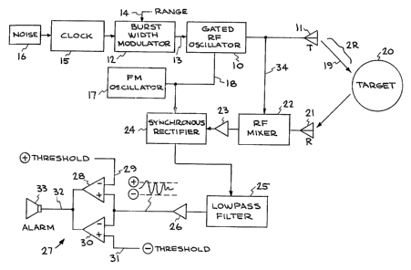
Fig.1 is a block diagram of the range~ated field disturbance sensor
of the present invention.
-6a-
WO 96107931 ~ '~ ~ ~ PCTIUS95/11046
Fig. 2 is a timing diagram illustrating the frequency modulation
features of the present invention.
' Fig. 3 is a timing diagram illustrating the mixing and range-gating
operation of the present invention.
Fig. 4 is a plot showing the performance of i:he sensor according to
the present invention.
Fig. 5 is a schematic diagram of one embodiment of the sensor
according to the present invention.
Fig. 6 is a schematic diagram of an alternative embodiment of the
sensor according to the present invention.
Fig. 7 is a schematic diagram of a battery power supply for use with
the circuit of Fig. 6.
Fig. 8 is a table of component values of Fig. 6 at two transmitter
frequencies.
DETAILED DESCRIPTION
A detailed description of embodiments of the present invention is
provided below with respect to the figures.
Fig. 1 is a block diagram of a range-gated field disturbance sensor
with range sensitivity compensation according to the present invention.
The basic system includes a gated RF oscillator 10 which drives a
transmitting antenna 11. The gated RF oscillator 10 generates a sequence
of bursts having a burst width determined by a burst width modulator 12
which is connected across line 13 to the gated RF oscillator. The burst
width modulator 12 defines a burst width in response to an input control 14
to select the range ef the device. The burst repetition rate is determined
by a clock 15 which drives the burst width modulator. Clock 15 is phase
modulated by a random source 16, such as noise which may be amplified
_7_
WO 96107931 - i PCTlUS95/110~
to produce a modulation signal, or may be inherent in the burst repetition
rate oscillator. Also, pseudo random modulation may be used.
The gated RF oscillator 10 is frequency modulated by an
intermediate frequency source 17 connected to the gated RF oscillator 10
across line 18.
The transmitted burst 19 reflects off a target 20 and the echo is
detected by a receive antenna 21. The receive antenna 21 drives an RF
mixer 22, which is also coupled to the transmitted signal, as schematically
illustrated by line 34. The output of the RF mixer 22 is coupled to an
intermediate frequency amplifier 23 which is tuned to the frequency of the
FM intermediate frequency source 17. The output of the intermediate
frequency amplifier 23 is coupled to a synchronous rectifier 24, which is
synchronized by the FM intermediate frequency source 17. The output of
the rectifier 24 is supplied through a lowpass filter 25 and baseband
amplifier 26 to a threshold detection circuit, generally 27. The threshold
detection circuit comprises a first comparator 28 having a negative input
coupled to a positive threshold value 29, and a positive input coupled to the
output of the baseband amplifier 26. Also, the threshold detector includes
a second comparator 30 having a negative input coupled to the output of
the baseband amplifier 26 and the positive input coupled to the negative
threshold 31. When the amplitude of the output of the baseband amplifier
26 exceeds the thresholds, an alarm signal is supplied on line 32 to drive
an alarm circuit, such as a beeper 33 or other responding apparatus. The
beeper 33 may be replaced, for instance, by a switch which drives a wide
variety of responding apparatus.
Also, rather than driving a threshold detectionlalarm circuit, as
illustrated in Fig. 1, the output of the baseband amplifier may be digitized
_g_
WO 96107931 2 '~ . g g 1 2 1 pCT~s95/11046
and processed to determine the characteristics of the disturbance shown
in the received signals, such as velocity of motion, size, etc.
In one designed system, the gated RF oscillator generates a burst
of about 2 gigaHertz. The FM oscillator 17 operates at about 10KHz, and
modulates the output frequency of the oscillator 10 between, for instance,
2.OOGHz and 2.10GHz. The burst repetition frequency defined by the
oscillator 15 in this embodiment is about 2MHz. The noise source 16
preferably modulates the phase of the burst repetition frequency oscillator
over an equivalent range substantially greater than the burst width.
10 The burst width defines the range of the device, because RF mixing
at the mixer 22 only occurs during transmission of the burst. In the 2GHz
system mentioned above, the burst width may be on the order of 2 to 40
cycles or so of the gated RF oscillator 10, providing a low duty cycle for the
transmitter, and therefore a low power consumption. At a 2GHz transmitter
15 frequency, and a range of about 12 inches, the burst width should be about
4 cycles, or about 2 nanoseconds.
Fig. 2 illustrates certain characteristics of the bursts in the sequence
of bursts. As illustrated in Fig. 1, the RF oscillator is frequency modulated
with a squa~ a wave at approximately 1 OKHz. Thus, the burst will be
g~:nerated wit's a first low frequency f~, and a second high frequency fH.
Ft~ecluenc? .r are only slightly different from one another as illustrated in
Fig.
2.'~~'4Tf~us, in the near range, such as after four cycles, the difference in
ptEase at a given distance befween the two frequencies (04~N) is very slight.
However, at the end of the burst, the difference in phase at the end of the
burst bafiween the two frequencies (~~F) is about 180°. Thus, the head
60
of the burst at frequency fN is about in phase with the tail 61 for a given
burst width for a relative phase shift of about 0°. In contrast, the
head 62
of the burst at frequency fL is about 180° out of phase with the tail
63 for a
_g_
WO 96/07931 _ ~ PCTIUS95/110d~
relative phase shift of about 180° at the same burst width. This
provides
a full 180° phase reversal at the intermediate frequency in the echo
received from objects at the maximum range based on the 180° relative
phase shift difference.
The sensor, according to a preferred embodiment, has a relative
phase shift difference of less than 360° and, for best results, less
than
about 180°, between the two RF frequencies at the maximum sensor
range.
The sensors, according to the present invention, are operational
even with a relative phase shift difference of more than one cycle.
However, when the relative phase shift difference is greater than
180°, the
sensitivity of the device will be reduced. Also, if the relative phase shift
difference at a particular range falls to zero, then blind spots may be
created within the sensor field. Thus, in the preferred system, which has
an adjustable burst width, the frequency modulation is set so that at
maximum range the relative phase shift difference is about 180°, so
that
as the range is tuned by shortening the burst width, the relative phase shift
difference is less than 180°. For very short range operation, the
relative
phase shift difference will be slight. The particular relation selected for a
given design will depend on the characteristics of the field in which the
sensor is deployed, and the components used to implement the sensor.
Thus, for instance, there may be N cycles-.at the transmitted
frequency f~, for a given burst width. For this embodiment, at the
transmitted frequency fH, there may be N+1I2 cycles in the burst width for
the higher frequency. Of course, the absolute number of cycles in a burst
will vary depending on the circuits used to generate the bursts. But the
phase relationship can be enforced by controlling the transmitter
frequency.
-10-
WO 96/07931 ~ PCT/US95/11046
Fig. 3 illustrates the mixing function of the received cycle. Thus, in
Fig. 3, the trace 50 illustrates the transmitted burst. The trace 51
illustrates
a receive reflection. Trace 52 illustrates the period during which mixing
occurs. That is, mixing occurs from the beginning of the reception of the
reflected signal at point 53 until the end of the transmitted signal at point
54.
Also illustrated at trace 52 are the magnitudes of the received
echoes at the low frequency f~ and at the higher frequency fH. This
difference in amplitude DA is a function of the distance at which the
disturbance occurs as reflected in the difference: in phase between the
transmitted burst and the received reflections, as well as the magnitude of
disturbance. In the actual system, the intermediate frequency signal is
based on integrating a large number of the mixed signal pulses, oscillating
between the fH and f~ values at the intermediate frequency. Thus, at very
close ranges, the differences in magnitude due to the frequency
modulation for a given magnitude of disturbance will be lower than the
difference in magnitude of the mixed signal at longer range.
Fig. 4 illustrates the performance of the sensor over its set range,
showing that the sensitivity d~ne~ not increase substantially at close range.
Thus, in Fig. 4, tire intermediate frequency response sampled at the output
of the baseband amplifier 26, for instance, is illustrated. With the range set
at about 12 inches, this signal was generated by moving a hand in to touch
the transmitter aid then back out. As can be seen at the close range at
point 70, the amplitude of the signal is not substantially greater than at
about 6 inches at point 71. Fig. 4 also illustrates that outside the range,
. there is little intermediate frequency signal generated.
Fig. 5 is an electrical schematic diagram of a sensor according to
the present invention which was used in generation of the plot of Fig. 4.
-11-
WO 96107931 PCTlUS9511104
The transmitter is driven by a radio frequency transistor 100 which is
biased to oscillate at the transmitter frequency. The collector of the
transistor 100 is coupled to antenna 101, and across an inductance 102 -
(simply inherent in the physical layout) to bias node 103. The bias node
103 is coupled across a capacitor 104 to ground, and through resistor 105
to an FM oscillator composed of inverter 106 and inverter 107. The
inverter 106 drives the output of the FM oscillator, and is connected in
feedback across capacitor 108 to the input of inverter 107. Also, the output
of inverter 107 is coupled across resistor 109 to its input.
Node 103 is also connected across resistor 110 to capacitor 111
which is coupled on its opposite terminal to ground. The cathode of diode
112 is coupled to the capacitor 111, and ifs anode is coupled to the
cathode of diode 113. The anode of diode 113 is coupled to a 5 volt
supply. Also, the anode of diode 112 and the cathode of diode 113 are
coupled across capacitor 114 to the output of inverter 115. The input of
inverter 115 is coupled to the burst repetition frequency oscillator set at
about 2MHz, composed of inverter 116 and inverter 117. The output of
inverter 116 is coupled to the input of inverter 115, and across capacitor
118 to the input of inverter 117. Also, the output of inverter 117 is
connected across resistor 119 to its input.
A variable resistance composed of potentiometer 120 in series with
resistor 121, and parallel resistor 122 are coupled from the output of
inverter 117 to the input of inverter 123. Also, the input of inverter 123 is
connected across capacitor 124 to ground. The output of inverter 123 is
connected across resistor 199 to the emitter of the oscillating transistor
100. Also, capacitor 125 is connected from the emitter of transistor 100 to
ground.
-12-
WO 96/07931 = ~ 1 c~ g ~ ~ ~ PC"TIUS95l11046
The base of transistor 100 is driven through inductor 126 by the
output of inverter 116 at the burst repetition rate frequency.
' In operation, the frequency of oscillation of the transistor 100 is
varied by the bias at node 103. This bias is modulated at 7KHz by the
oscillator composed of inverters 107 and 106. The: transistor 100 oscillates
when the base to emitter voltage is above its threshold. This occurs on the
rising edge of the output of inverter 116 for short burst length determined
by the delay induced by the RC network composed of resistors 120
through 122 and capacitor 124, as driven through inverter 123. Thus,
when the output of inverter 123 rises, the difference in voltage between the
base and emitter of transistor 100 falls below the threshold, turning off the
oscillator. Thus, on the rising edge of the output of inverter 116, a short
burst is emitted by antenna 101 having a burst length which can be
adjusted by adjusting potentiometer 120. Thus, this circuit sets the burst
length for the transmitter circuit. Unwanted variations in burst width are
minimized when inverters 116 and 123 are matched through common
monolithic integration. With a 2MHz burst repetition rate and a 7KHz
frequency modulation rate, there are about 6500 bu~sfs per IF cycle.
The receiver includes receiving antenna 150 which is coupled to
node 151. From node 151, an inductor 152 is coupled to ground. Also, the
cathode of Schottky diode 153 is coupled to node '151. The anode of diode
153 is connected across capacitor 154-to ground and across resistor 155
to a positive 5 volt supply, and is coupled through capacitance 156 to an
intermediate frequency transistor 157 connected as an amplifier. Thus, the
base of transistor 157 is connected across resistor 158 to ifs collector.
Also, the collector is coupled across resistor 150 to a 5 volt supply. The
emitter of transistor 157 is connected to ground. The collector of transistor
157 is connected through capacitor 160 to an intermediate frequency
-13-
WO 96/07931 ~ ~ ~ ~ ~ PCTlUS95/1104y
amplifier composed of inverter 161 with resistor 162 connected in
feedback. The output of inverter 161 is connected to a sample and hold
circuit composed of transistor 163 having its base connected across -
resistor 164 to the output of inverter 107 in the FM oscillator. The collector
of transistor 163 is connected to a first terminal of capacitor 165. The '
second terminal of capacitor 165 is connected to ground. Aiso, the
collector of transistor 163 is connected through capacitor 166 and resistor
167 to the input of inverter 168 which is connected as a baseband
amplifier. The resistor 169 and capacitor 170 are connected in parallel and
in feedback across inverter 168. The output of inverter 168 is connected
across resistor 171 to the input of inverter 172 which is connected as an
amplifier with resistor 173 and capacitor 174 in parallel and in feedback.
The output of inverter 172 is connected through capacitor 175 and resistor
176 to the input of inverter 177. Resistor 178 is connected in feedback
across inverter 177. The output of inverter 177 drives a threshold detection
circuit. The input of the threshold detection circuit is node 198. A first
resistor 179 is coupled between node 198 and the input of inverter 180.
Also, resistor 181 is connected between the input of inverter 180 and a 5
volt supply. A second resistor 182 is connected between node 178 and
inverter 183. Also, resistor 184 is connected between the input of inverter
183 and ground. The output of inverter 180 is connected through diode
185 to node 186. The output of inverter 183 is connected through inverter
187 and diode 188 to node 186. Node 186 is connected across RC
network composed of resistor 189 and capacitor 190 to the gate of
transistor 191. Also, resistor 192 is connected between the gate of
transistor 191 and ground. The source of transistor 191 is connected to
ground, the drain of transistor 191 is connected through resistor 193 to a
-14-
WO 96/07931 ~ PCT/L1S95111046
beeper 194 which is biased with resistor 195 and bypassed with capacitor
196.
Thus, in operation, the transmitted signal is coupled to the receiving
antenna by proximity of the transmitter and receiver. The reflected signal
is received by the receive antenna and mixed at diode 153. Each cycle of
the mixed signal is sampled by diode 153, and charges capacitor 154 to
the magnitude of the sampled signal. The magnitude of the voltage on
capacitor 154 will vary at the intermediate frequency as described above.
This intermediate frequency signal is coupled through the amplifier
composed of transistor 157 and inverter 161 to the sample and hold circuit
driven by transistor 163. The transistor 163 is synchronized with the
modulation frequency of the transmitter to sample and hold the average
magnitude of the mixed signal. The average magnitude is amplified and
supplied to a peak detection circuit. By setting the trip value on the peak
detection circuit, the sensitivity of the sensor can be selected.
In the preferred system, the transmitting and receiving antennae 101
and 150 are formed with 1-1/2 inch lengths of wire arranged in a dipole for
a 2GHz transmitter frequency, and positioned so that the transmitie~i signal
is coupled to the receiving antenna with a magnitude sufficient for the
mixing operation.
The burst repetition frequency generator is ~ modulated by noise
inherent in the inverters selected for the embodirn~:nt illustrated in Fig. 5,
so no additional modulation circuitry is necessary.
With the component values illustrated in the figure, this circuit is
range tunable from about zero to about 12 feet. T'he modulation of the RF
oscillator is set for approximately 180° phase reversal at the maximum
range.
-15-
WO 96107931 _ ~ PCT/US95/1104~
Fig. 6 illustrates an alternative embodiment of the range-gated
proximity sensor according to the present invention. In this embodiment,
the RF oscillator is driven by transistor 200. The base of transistor 200 is
connected to ground through inductor 254. The emitter of transistor 200
is connected across capacitor 201 to ground and across resistor 202 to
node 203. Node 203 is connected across resistor 204 to ground and
across capacitor 205 to a 2MHz burst repetition rate oscillator. This
oscillator includes inverter 206 and inverter 207 connected in series. The
output of inverter 207 is connected to capacitor 205, and across capacitor
208 to the input of inverter 207. Also, the output of inverter 207 is
connected across resistor 209 to ifs input.
The collector of transistor 200 is modulated through inductor 255 by
the signal at node 210 which is connected across capacitor 211 to ground
and across resistor 212 to a 5 volt supply. Also, node 210 is connected
across resistor 213 to the output of the modulating oscillator which is
composed of inverters 214 and 215 in series. The output of inverter 214
is connected across capacitor 216 to the input of inverter 215. Also, the
output of inverter 215 is connected across resistor 217 to its input.
The receiver shares the antenna 218 which is driven by the
oscillator 200. Thus, the receiver comprises Schottky diode 219 having its
anode connected to antenna 218. The cathode of diode 219 is connected
to node 220. Capacitor 221 is connected from node 220 to ground.
Resistor 222 is connected from node 220 to ground. Also, node 220 is
connected through capacitor 223 and resistor 224 to an amplifier
composed of inverter 225 with resistor 226 connected in feedback. The
output of inverter 225 is connected across resistor 227 to the input of
inverter 228. The output of inverter 228 is driven through diode 229 to
node 230. Resistor 231 is connected from node 230 to the input of inverter
-16-
WO 96/07931 s PCT/U595I11046
228. Also, capacitor 232 is connected from node 230 to ground. Node 230
is connected through capacitor 233 and resistor 234 to the input of inverter
235. The voltage at node 230 is the peak detected value of the IF signal
supplied by IF amplifier 225. Resistor 236 is connected in feedback from
the output of inverter 235 to its input. Also, the output of inverter 235 is
connected across resistor 237 to the input of inverter 238. The output of
inverter 238 has resistor 239 and capacitor 240 coupled in parallel and in
feedback. The output of inverter 238 is connected through capacitor 241
and resistor 242 to the input of inverter 243. Inverter 243 has resistor 244
and capacitor 245 connected in feedback. The output of inverter 243 is
connected through capacitor 246 and resistor 247 to node 248. Node 248
is also connected across resistor 249 to ground. Also, the output of
inverter 243 is connected through resistor 250 to the input of inverter 251.
The input of inverter 251 is connected across resistor 252 to the positive
supply. The output of inverter 251 is a signal on line 253 indicating
detection of a disturbance in the field. Also, node 248 may be used to
drive such alarm circuitry as desired.
This circuit of Fig. 6 is driven by a power supply such as shown in
Fig. 7. Thus, a 9 volt battery 275 is connected through a power switch 276
to a converter circuit which includes capacitor 277 coupled from the switch
276 to ground, and a voltage converter circuit 278 laving an output 279 of
about 5 volts. Also, the output 279 is connected across capacitor 280 to
ground. The 5 volt supply is used to drive the circuitry illustrated in Fig.
6.
The frequency of the transmitter can be adjusted as suits the needs
of a particular design. For a 2GHz center frequency, the values of labelled
components are illustrated in Fig. 8. Also, for a 6.5GHz center frequency,
values illustrated in Fig. 8 can be used.
-17-
WO 96/07931 PCT/U895/110~4~
2~9~1~1
The circuit designs illustrated in Figs. 5 and 6 are composed of off
the-shelf components readily available to persons of skill in the art,
examples of the values of which are shown in the figures. it will be
recognized that these circuits may be provided in application specific
integrated circuits (ASICs), or in other combinations of components as suits
the needs of a particular designer.
The embodiments described herein have RF transmitters which are
frequency modulated at an intermediate frequency. Alternative systems
may have amplitude modulated RF transmitters, or transmitters modulated
by other methods, using techniques known in the art of oscillator
modulation. For instance, the RF oscillator may be operated in a double
burst mode, where a first burst is transmitted followed by a second burst
with a fixed interval in between. The first burst will mix with the second
only
at a specific range determined by the inter-burst interval. This will save
average power output for longer ranges, while preventing disturbances at
closer ranges from being measured. Also, other envelope shaping
techniques could be employed for various effects.
CONCLUSION
Accordingly, the present invention provides a field disturbance
senses which is precisely range-gated, immune from interference from
--- neighboring sensors of the same type, or from other sources of noise, and
has compensation against hypersensitivity at close range. Further, the
circuit is very low power, enabling battery operation with long life. Thus, a
wide variety of new applications is provided for microwave based proximity
sensors, including, by way of example, proximity sensing car alarms, home
security systems, keyless entry systems, backup warning radar, and the
like.
-18-
WO 96/07931 - 1 ~ PCTlUS95/11046
The system is range-gated to limit the maximum detection range to
reduce false alarms with a typical adjustment range for the current
embodiments of 6 inches to 12 feet. The burst. repetition frequency is
noise coded to allow co-location of multiple sensors. The receiver is very
sensitive, allowing reduced transmit power. Thus, it need not operate in
the ISM bands which are crowded with other high powered microwave
users, such as microwave ovens. This results in a low operation current
with multiple year battery life possible, and very low manufacturing costs.
The low manufacturing cost is in part due to thE; low transmitted power
which avoids complex circuitry to comply with communications regulations.
Furthermore, the system is range sensitiv'~ty compensated, eliminating the
1/R2 characteristic of prior art systems. Thus, the system is not
hypersensitive at close range and maintains fairly constant sensitivity from
0 to the maximum range.
The foregoing description of prefer-ed embodiments of the invention
has been presented for purposes of illustration and description. It is not
intended to be exhaustive or to li(nit the invention to the precise forms
disclosed. Obviously, many modifications and variations will be apparent
to practitioners skilled in this art. It is intended that the scope of the
invention be defined by the following claims and their equivalents.
What is claimed is:
-19-