Note: Descriptions are shown in the official language in which they were submitted.
rv 2201695
-1-
Title: Phase Detector for High Speed Clock Recovery from Random
Binary Signals
FIELD OF THE INVENTION
The present invention relates to the field of data communications,
clock recovery, clock recovery of non-self clocking signals, phase-locked
loop clock recovery, phase detectors, and monolithic phase detectors.
Specifically, the present invention is a phase detector, suitable for
monolithic implementation, for use in a high speed phase-locked loop
1 0 clock recovery system for non-return-to-zero data signals.
BACKGROUND OF THE INVENTION
Serial digital transmission of non-self clocking or non-return-to-
zero (NIZZ) binary signals requires receiving circuitry to extract timing
1 5 information from the serial data to regenerate the clock. This recovered
clock is used to re-time the serial data for subsequent circuitry to receive
and process it synchronously. Most methods of clock recovery, especially
when implemented monolithically, use phase-locked loops (PLLs). The
PLL contains a voltage-controlled oscillator (VCO) which is controlled by
2 0 an integrated and low pass filtered output of a phase detector. The phase
detector output is representative of the phase difference between the input
serial data and the recovered clock, the latter being equal to or derived
from the VCO output.
The phase difference between an input NRZ data signal and a
2 5 locally generated clock signal can be obtained by generating a variable
control pulse signal proportional in width to that phase difference, in
addition to one or more other fixed width control pulses. The control
pulses are fed to control circuitry, such as a charge pump, which yields a
phase detector output signal. The phase detector output signal is filtered
3 0 and integrated to produce a phase error voltage signal which is then used
to drive the VCO: A phase detector such as this was disclosed in U.S.
Patent No. 4,535,459 by Hogge and modified in U.S. Patent No. 5,027,085 by
2201695
-2-
DeVito to reduce phase fitter caused by variations in data density.
While the input to the VCO directly controls the frequency of the
oscillator, frequency and phase are interdependent. For instance, a brief
pulse in a constant input to the VCO would alter the frequency only
momentarily but would subsequently result in a fixed change in the phase
of the output. Therefore, the phase of the VCO output signal will only
remain the same, before and after a series of changes in the VCO input
signal, if the average value of those changes is zero (or equivalently if the
average value of the integrated phase detector output signal does not
change).
A phase detector for this application must generate phase difference
information only when input data transitions occur. Ideally, the falling
edge of the clock coincides with a data transition, so that the data is phase
aligned for the rising edge of the clock to retime the data in the centre of
1 5 the data interval. This condition ensures the most stable and reliable
reading-in of the data. When it occurs there is said to be zero phase error,
and the phase of the VCO output should not change. Phase fitter, which
consists of spurious variations in the phase of the regenerated clock signal
must therefore be minimized.
2 0 While current phase detector circuits, for example that disclosed in
U.S. Patent No. 5,027,085 by DeVito, may provide zero static phase offset,
they do not provide zero phase offset in high speed applications where the
input serial data itself has sigrificant fitter (with respect to the clock)
and
where practical circuitry and subsequent circuitry have limited bandwidth.
2 5 The result is a reduction in input fitter tolerance. It is therefore an
object of
the present invention to provide a phase detector circuit which provides
minimal static phase offset in the presence of large input fitter, increases
the input fitter tolerance, and allows for the use of circuitry with lower
bandwidth and therefore with lower current consumption.
BRIEF SUMMARY OF THE INVENTION
In one aspect, the present invention provides a phase detector
2201695
-3-
circuit for detecting the phase difference between an information signal
and a clock signal and for producing a phase error signal representative of
said phase difference, said clock signal and said information signal being
pulse type waveforms having first and second levels and having first and
second edges, said information signal containing data at a certain data rate
and said first and second edges of said information signal being data
transitions, said phase detector circuit comprising: (a) a divider circuit for
dividing said information signal into a plurality N of divided signals, the
data rate of each of said divided signals being the data rate of said
1 0 information signal divided by N; (b) a pulse signal circuit coupled to
said
divider circuit for producing a plurality N of difference pulse signals, each
of said difference pulse signals being responsive to the phase difference
between one of said divided signals and said clock signal, the width of each
of said difference pulse signals being not less than the width between said
1 5 first and second edges of said clock signal, said pulse signal circuit
further
producing one or more reference pulse signals and the width of each of
said one or more reference pulse signals being integrally proportional to
the width between said first and second edges of said clock signal; and (c) a
phase error signal circuit coupled to said pulse signal circuit for producing
2 0 said phase error signal in response to said plurality of difference pulse
signals and said one or more reference pulse signals.
Preferably, said divider circuit divides said information signal into a
first divided signal and a second divided signal, the data rate of said first
divided signal and said second divided signal being one half the data rate
2 5 of said information signal, and said pulse signal circuit produces a first
difference pulse signal responsive to the phase difference between said first
divided signal and said clock signal, a second difference pulse responsive
to the phase difference between said second divided signal and said clock
signal, and said one or more reference pulse signals such that the time
3 0 average of the changes in said phase error signal is zero when the second
edge of said clock signal coincides with a data transition of said
information signal.
2201695
-4-
BRIEF DESCRIPTION OF THE DRAWINGS
In the accompanying drawings which illustrate preferred
embodiments of the present invention:
Fig. 1 is a block diagram illustrating a basic phase-locked-loop circuit
configuration used for clock recovery.
Figs. 2A and 2B show prior art phase detector circuits.
Fig. 3 is a timing diagram for the operation of Fig. 2A.
Fig. 4 shows the phase detector transfer function for the phase
1 0 detector of Figs. 2A or 2B.
Fig. 5 shows the time response of the phase detector of Figs. 2A or
2B.
Figs. 6 through 12 show several embodiments of the phase detector
circuit of the present invention.
1 5 Fig. 13 shows a frequency divider circuit for the input data signal.
Fig. 14 is a timing diagram of the frequency division signals.
Fig. 15 shows the output waveforms for the circuit of Fig. 9.
Figs. 16A and 16B illustrate the average of phase detector output
signals in relation to the average of the time integrals of those signals.
2 0 Fig. 17 shows the output waveforms for the circuit of Fig. 12.
Fig. 18 shows the phase detector circuit of Fig. 12 with control
circuitry in a phase-locked loop.
DETAILED DESCRIPTION OF THE PREFERRED EMBODIMENTS
2 5 Fig. 1 shows a basic circuit block diagram for a phase-locked loop
(PLL) 2 used to recover or regenerate a clock signal 12 from input serial
NRZ data 10. The phase detector circuitry 4 provides a plurality of control
pulse signals 5 to the control (summing) circuitry 6 which outputs a phase
detector output signal 50 in response. The phase detector output 50 is the
3 0 input to loop filter and integrator 7. The output 9 of loop filter 7 is
the
phase error voltage signal which drives a voltage controlled oscillator
(VCO) 8 whose output is essentially the recovered clock signal 12 which is
2201695
-5-
fed back to gate (i.e. control the timing of) the phase detector circuitry 4.
Figs. 2A and 2B show two versions of the prior art phase detector
circuit disclosed by Devito in U.S. Patent No. 5,027,085. Referring to Fig.
2A, an input data signal 10 is connected to the input of a delay or retiming
means 14, whose output 22 is connected to the input of a delay or retiming
means 16, whose output 24 is in turn connected to the input of a delay or
retiming means 18. The retiming means 14, 16, and 18 are all gated by
alternate edges or levels (depending on the type of retiming means used)
of the regenerated clock signal 12, which is derived from the phase detector
1 0 output 50. In Fig. 2A, the retiming means 14, 16, and 18 are shown as D
flip-flops and so are triggered by either the rising or falling edges of the
regenerated clock signal 12. As shown in Fig. 2A, D flip-flops 14 and 18 are
rising-edge triggered and D flip-flop 16 is falling edge triggered. The
retiming means could also each consist of a master and slave combination
1 5 of two D latches. It is obvious to those skilled in the art that the slave
latch
of one retiming means can perform the dual role of master latch in the
next retiming means, thus allowing for the omission of redundant latches.
In this manner, the retiming means 14, 16, and 18 can consist of a "series"
combination of 4 latches.
2 0 The control pulse signals UP1 38, DOWN 40, and UP2 42 are
generated by exclusive-OR (XOR) gates 30, 32, and 34 respectively. The
inputs to XOR gate 30 are the input data signal 10 and the output 22 of
retiming means 14. The inputs to XOR gate 32 are the output 22 of
retiming means 14 and the output 24 of retiming means 16. The inputs to
2 5 XOR gate 30 are the output 24 of retiming means 16 and the output 26 of
retiming means 18. Before being fed to a control summing circuit 6, the
DOWN signal 40 is doubled at the multiplier 46. At the summing circuit 6,
the UPl signal 38 and the UP2 signal 42 are summed positively and the
DOWN signal 40 is summed negatively. The output of the summer is the
3 0 phase detector output 50 from which the regenerated clock signal 12 is
derived.
The circuit of Fig. 2B shows the phase detector of Fig. 2A with an
2201695
-6-
additional retiming means 20 whose input is the output 26 of retiming
means 18. A fourth control pulse signal 44 is generated by XOR gate 36
whose inputs are the output 26 of retiming means 18 and the output of
retiming means 20. The presence of an additional control signal 44
obviates the requirement of doubling the DOWN control signal 40 before
summing.
Fig. 3 shows a timing diagram for the operation of the circuit of FIG.
2A. In Fig. 3, the data (or bit) rate for signal 10 is lower than the
frequency
of the clock signal 12. For the purpose of illustration, the clock signal 12
is
also shown as a constant frequency and phase signal. In operation,
however, the clock signal will change in response to the phase detector
output signal 50 when the time average of the changes in the filtered and
integrated phase detector output signal (the phase error signal) is non-zero.
Referring to Fig. 3, it is observed that the UP1 pulses can vary in
1 5 pulse width between zero and one period of the clock signal 12. As the
input data lags the clock, the positive UP1 pulses become more and more
narrow. In practical XOR gates and control circuits, such as charge pumps,
there is a limit for the response time of the circuit which results in
effectively narrowing or eliminating input pulses which are too narrow.
2 0 Therefore, as the UP1 pulses become narrower and narrower, they are
ultimately filtered out and do not provide any pulse information for
driving the VCO. In such cases and also in the case of high speed
applications, the phase detector transfer function has a non-linearity
which is shown in Fig. 4. As described below, this non-linearity can cause a
2 5 significant reduction in input fitter tolerance for the phase detector
circuits
of Figs. 2A and 2B.
Referring to Fig. 4, The non-linearity of the phase detector transfer
function is not symmetrical about the phase difference between the input
data and clock signals (ei-eo) axis 52, and results in a non-zero average
3 0 phase detector output when the phase difference has large enough
amplitude. Fig. 5 illustrates the low pass filtered time response of the non-
linear phase detector transfer function to an input in which the data rate
2201695
equals the clock frequency and the two signals have a sinusoidal phase
difference 54. The non-linear distortion 56 results in an average negative
phase detector output. When this occurs, the PLL circuit responds by
decreasing the phase of the VCO output or clock until the average phase
error is zero. As a result, a phase offset will occur in the presence of large
input fitter, which, in turn, translates into a reduction in input fitter
tolerance.
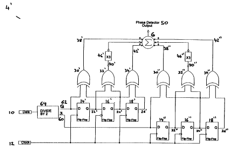
Figs. 6 through 12 show several possible embodiments of a phase
detector circuit 4' of the present invention. In all of the illustrated
1 0 embodiments of the present invention, the input serial data is initially
frequency divided by two, resulting in an "in-phase" data signal I and a
data signal Q in "phase quadrature" with the input signal 10. Fig. 13 shows
an example of a circuit 64 which performs the dividing function via
latches 66 and 68, and Fig. 14 is a timing diagram of the signals involved,
1 5 ignoring propagation delays. The signals I 60 and Q 62 effectively contain
every other data transition from the input signal 10. The data signal I 60
toggles at each rising edge of the signal 10, and the data signal Q 62 toggles
at each falling edge of the signal 10, so that when the signal 10 is low I and
Q are at the same level and when the signal 10 is high I and Q are at
2 0 different levels. As a result, the original input data signal can be
regenerated by an XOR function of the two divided data signals, as shown
at 64 in Fig. 11. Alternatively, the input serial data could also be frequency
divided by an integral number greater than two and then recombined in a
manner similar to that just described.
2 5 Referring back to Fig. 6, a first embodiment of the present invention
is shown which divides at 64 the input signal 10 and then processes each
divided signal 60 and 62 through a series of retiming means, shown in Fig.
6 as flip-flops. The independent processing of each divided 60 and 62 signal
is similar to the processing of the complete input data signal 12 which took
3 0 place in Fig. 2A. T'he signal Q 62 passes through three retiming means
14',
16', and 18' and generates three control pulse signals 38', 40' and 42' via
XOR gates 30', 32', and 34'. The signal I 60 passes through another three
2201695
_8.
retiming means 14", 16", and 18" and generates three control pulse signals
38", 40" and 42" via XOR gates 30", 32", and 34". The retiming means are
gated by alternate edges (if the retiming means are flip-flops) or alternate
levels (if the retiming means are slave-latch combinations) of the clock
signal 12. Corresponding retiming means in each processing stream are
similarly gated. For example and as shown in Fig. 6, the flip-flops 14', 14",
18', and 18" are rising edge triggered and the flip-flops 16' and 16" are
falling edge triggered.
To eliminate the non-linearity present in the phase detector of Figs.
1 0 2A and 2B, the inputs to the XOR gate 30' are the signal Q 62 and the
output 24' of the retiming means 16'. Similarly, the inputs to the XOR gate
30" are the signal I 60 and the output 24" of the retiming means 16". As a
result, the signals 38' and 38" have a minimum pulse width of one half of
a clock period. Due to the lengthening of the 38' and 38" pulses the
1 5 multipliers 46' and 46" multiply by three as compared to by two in Fig 2A.
The resolution of control signal pulses for consecutive data transitions in
the input signal 10 remains possible, in spite of the lengthening of the
pulse widths of signals 38' and 38", because of the initial frequency
division of that signal.
2 0 The phase detector circuit of Fig. 6 can be reduced to the circuit of
Fig. 7, as will be obvious to one skilled in the art. Referring to Fig. 7, the
once retimed data input signal 22 is produced or recombined by an XOR
function at 70 of the once retimed divided input signals 22' and 22".
Similarly the twice retimed data input signal 24 is produced or recombined
2 5 by an XOR function at 72 of the twice retimed divided input signals 24'
and
24". This allows retiming means 18 and XOR gates 32 and 34 to function as
already described in Fig. 2A. The XOR gate 74 is necessary to match the
propagation delay of XOR gate 72 (so that the width of control pulse 42 is
one-half a clock period, with the accuracy of that value depending on the
3 0 matching of the delay through gates 72 and 74), but otherwise XOR gate 74
does not affect the functionality of the phase detector circuit.
Fig. 8 shows a similar embodiment to the circuit of Fig. 7 where an
2201695
-9-
additional retiming means is added in the same manner that the circuit
of Fig. 2A was extended into the circuit of Fig. 2B, as already described
above. Fig. 9 shows the phase detector circuit of Fig. 7 implemented with
gated D-type latches replacing the flip-flops of Fig. 7 as the retiming means,
in the manner explained above. In Fig. 9, latch 92 acts as a slave latch to
both latches 84 and 90. Other similar functional implementations, such as
of the circuits of Fig. 6 or 8 with gated D-type latches replacing the flip-
flops
as retiming means, will be obvious to those skilled in the art.
The phase detector outputs 50 of the circuits of Figs. 7, 8 and 9, while
1 0 theoretically (i.e under ideal conditions) similar to that of Fig. 2A, do
not
suffer from many of the practical limitations (caused by the limits in XOR
gate and control circuit response time) present in the prior art. Fig. 15
shows the output waveforms for the circuit of Fig. 9. Three UP signals 38',
38", and 42 and one DOWN signal 40 are summed to produce the phase
1 5 detector output 50. UP1 38' is produced on every other input data signal
transition, and UP2 38" is produced on all other data transitions. Since the
occurrence of the UP1 38' or UP2 38" signal is half the frequency of that of
the prior art (see signal 38 in Fig. 3), these signal pulses are made wider by
one-half a clock period. As already indicated, this is achieved by making
2 0 the XOR input connection across three latches (or two flip flops) versus
two (or one) in the prior art. As illustrated at 94 in Fig. 5 neither UP1 38'
nor UP2 38" becomes more narrow than one-half a clock period when a
pulse in the phase detector output signal is very narrow. Thus, there is no
distortion introduced to the phase detector transfer function.
2 5 The XOR gate 72 in Fig. 7, 8 or 9 can also be replaced with an
appropriately gated retiming means with its input connected to the output
of XOR gate 70 (signal 22), its output connected to the input to flip flop 18
in Figs. 7 and 8 or to latch 92 in Fig. 9 (signal 24), and its clock input
connected to the output of XOR gate 74.
3 0 Fig. 10 shows such an implementation for the circuit of Fig. 9 with
the XOR gate 72 replaced by the latch 91. In Fig. 10, which is a preferred
embodiment of the present invention, XOR gate 74 matches the delay
2201695
-10-
through the XOR gate 70. Delay means 96, 98, 100, and 102 are also added to
the circuit of Fig. 10 to correct for the set-up time and propagation delay of
the latches 80, 82, 86, and 88. Delay means 96 and 98 each provide for a
delay equivalent to one data latch and may consist of a permanently
enabled data latch. Delay means 100 and 102 each provide for a delay
equivalent to two data latches and may consist of a combination of two
permanently enabled data latches.
Delay means 96, 98, 100, and 102 can be added to the circuits of Figs. 6
through 9 in the same manner as illustrated in Fig. 10 to correct for the
1 0 inherent delays present in the retiming means of those circuits. With
these delay means added to it, the circuit of Fig. , 9 is functionally
equivalent to the circuit of Fig. 10.
In another embodiment of the present invention, the circuit of Fig.
can be reduced to the circuit of Fig. 11 in which latch 92 is removed and
1 5 only two retimings of the input data signal 10 effectively take place.
Referring to Fig. 11, the XOR gates 32' and 32" perform the same function
as the identically labelled gates in Fig. 6 in generating signals 40' and 40"
respectively. In the Fig. 11 embodiment of the present invention, the
DOWN signal 40 is generated by an OR function at gate 104 of the signals
2 0 40' and 40". Because a data transition in one of the divided data signals
always occurs at least one data interval apart from a data transition in the
other divided data signal, and because the clock frequency must be at least
twice high as the data or bit rate, the pulse signals 40' and 40" are never
high at the same time and OR gate 104 effectively sums these two signals.
2 5 Also, since the circuit of Fig. 11 generates the DOWN pulse 40 without
using XOR gate 70, the need for a delay via XOR gate 74 in Fig. 10 is
obviated.
When an input data transition occurs with zero phase error, the
phase of the VCO output should not change, and therefore the average
3 0 value of the phase error signal or VCO input (i.e. the filtered and
integrated phase detector output signal) should not change. However,
while the average change in the phase detector output signal 50 in
2201695
-11-
response to an input data transition may be zero, the average change in the
integrated phase detector output (the phase error signal 9 in Fig. 1) may
still be non-zero. This concept is illustrated by way of example in Figs. 16A
and 16B. As a result, for phase detector outputs such as that shown in Fig.
16A, a non-zero phase offset will result when there are variations in the
density of input data transitions. This "pattern dependent fitter" may occur
in wideband systems.
Unlike the phase detector circuits of Figs. 6 through 10 which do not
suffer from pattern dependent fitter (this can be seen, for example, by the
1 0 form of the phase detector output waveform in Fig. 15 at time 95), the
phase detector output of the circuit of Fig. 11 does suffer from this
drawback. To solve this problem, the phase detector circuit of Fig. 11 is
further modified into the circuit of Fig. 12.
In the circuit of Fig. 12, which is a preferred embodiment of the
1 5 present invention, the OR gate 104 (and the delay through it) is removed
and the summing of the DOWN pulses 40' (DOWN1) and 40" (DOWN2)
takes place at the control summing circuit 6. Delay means 104 and 106, each
providing a delay of one-quarter of the clock period are also added to delay
the arrival of the UP1 and UP2 signals at the summing circuit 6 relative to
2 0 the DOWN pulses. The phase detector circuit of Fig. 12 is advantageous
when a phase detector circuit is to be used in a single clock frequency PLL
system, since the delays 104 and 106 are fixed value delays which are easily
implemented. The circuit of Fig. 12 may also be used in a multi-clock
frequency PLL system, but the delay means 104 and 106 are variable and
2 5 therefore more complex.
Fig. 17 shows the output waveforms for the circuit of Fig. 12. As
shown at 108 in Fig. 17, when the circuit is phase-locked (i.e. there is no
phase error) the corresponding UP and DOWN pulses overlap so that the
phase detector output pulses one unit high for one-quarter clock period,
3 0 pulses one unit low for one-half clock period, and pulses one unit high
again for one-quarter clock period. In the prior art circuit of Fig. 2A and in
the Figs. 6, 7, 9 and 10 embodiments of the present invention, a phase
2201695
-12-
locked phase detector output pulses one unit high for one-half clock
period, pulses two units low for one-half clock period, and pulses one unit
high for one-half clock period. As a result, the circuit of Fig. 12 produces a
lower peak-to-peak voltage signal on the loop filter and therefore less fitter
than in the prior art. This lower peak-to peak voltage signal is also
achieved by the prior art circuit of Fig. 2B and the circuit of Fig. 8 in the
present invention, but at the expense of requiring supplemental circuitry
to generate an additional control pulse signal as well as the expense of
requiring a longer time interval to measure phase error.
1 0 The complete phase detector for the preferred embodiment in Fig.
12 with charge pump control circuitry 6 is shown in a phase-locked loop in
Fig. 18. The control pulse (UP and DOWN) signals are used to control, by
way of switches 120, 122, 124, and 126, the charge pump 6 which comprises
current sources 112, 114, 116 and 118 working into a loop filter 7 which
1 5 processes the phase detector output signal and which may comprise a
resistor-capacitor network. The filter 7 achieves both the integration of the
current signal pulses and a low pass filter function to define the PLL
bandwidth. Similarly to the XOR gates which generate the control pulses,
the switches 120, 122, 124, and 126 in the charge pump 6 have limited
2 0 bandwidth and thus require control pulses of some minimum width.
Since there is no circuitry associated with the summing function in this
implementation, further bandwidth limiting the narrow output pulses of
the phase detector output is avoided. The summing function is simply the
connection of the current sources into one common node 110 where the
2 5 loop filter 7 is connected. Although node 110 is shown as single-ended,
the
specific configuration, whether single-ended or differential, is not
significant. Similar charge pump summation circuitry can be
implemented for any embodiments of the present invention.
The charge pump 6 receives a net positive (or UP) pulse when the
3 0 clock lags the input serial data and dumps a net positive charge packet
into
the resistor-capacitor network (loop filter) 7 to increase the VCO frequency.
Where no input serial data transitions occur, no charge is added or
2201695
-13-
removed from the loop filter 7, and the VCO frequency remains
unchanged. Therefore, only when input data transitions occur, does the
phase detector provide control signal pulses of net width proportional to
the phase difference of the input data and clock signals.
The feedback of the PLL 2 will force the pulse widths of UP1 38' and
UP2 38" to equal twice that of the DOWN1 and DOWN2 pulses 40' and 40"
(for example, at 108 in Fig. 17.) The width of the DOWN pulses is one-half
the clock period, and the accuracy of that value depends on the matching
of the delay from the clock input to the output of D latches 82 and 84 for
1 0 DOWNl and from the clock input to the output of D latches 86 and 88 for
DOWN2. In order to achieve zero static phase offset, the width of UPl and
UP2 depend on the matching of the gate delays for the arrival of each of
the inputs to XOR gates 30' and 30" respectively, and are determined by the
time from a data transition to a positive clock edge plus one-half a clock
1 5 period. Therefore, the PLL 2 locks when the time from a data transition to
a positive clock edge equals one-half a clock period.
The value of Iupl 112 and Iup2 114 must equal one-half the value
of Idownl 116 and Idown2 118 to ensure the condition of zero static phase
offset. The clock output 76 is synchronized to the regenerated data 78 (Data
2 0 Out) so that the positive edge of the clock occurs one-half a data bit-
period
after the data transition.
It should once again be noted that the present invention is not
limited to embodiments which frequency divide the input data signal by
two but rather may generally include frequency division of the input by an
2 5 integer N which is greater than two, so as to provide a plurality of N
divided signals. Preferably, the number of divided signals N is a positive
integer power of two (i.e. N equals 2M where M is a positive integer so that
N may equal 2, 4, 8, etc.) since the N divided signals may then be obtained
by further dividing each signal in a preceding set of divided signals (until
3 0 the required number of divided signals is obtained) in the same manner
that the initial set of divided signals was obtained. Note that if the widths
of the control pulses are lengthened, it will be necessary to frequency
._ 22016 95
-14-
divide the input signal by a number greater than two in order to ensure
the resolution of consecutive data transitions in the input signal.
While preferred embodiments of the invention have been
described, it will be realized that the embodiments disclosed are
illustrative and not restrictive, and that all changes within the meaning
and spirit of the invention are intended to be embraced by the appended
claims.