Note: Descriptions are shown in the official language in which they were submitted.
CA 02205851 2004-09-03
1
SIGNAL PROCESSING
FIELD OF THE INVENTION
The present invention relates to apparatus for, and method of, processing a
signal
received from an array of elements of a detector, and is particularly
applicable to
infra-red linear and two dimensional staring arrays and, especially, uncooled
staring
array sensors.
BACKGROUND OF THE INVENTION
Modern infra-red sensors utilise a large number of detector elements to detect
radiation
and produce an electronic signal from which a thermal image or other
information can
be obtained. A major problem associated with such multi-element systems is
that every
element in the detector array has a unique response and offset associated with
it, and
these must be normalised to some common level for further processing or image
display
to be performed. Frequently, the response can vary by over 50%, and the offset
by
several thousand equivalent degrees centigrade, from element to element. In
addition,
some higher order, non-linear variations between elements are frequently
present. The
non-uniformity correction processing circuit must be able to cope with these
large ranges
of transfer without introducing additional noise or distortion into the
signal.
Several approaches to cornecting detector non-uniformity have been developed
over the
years. The most obvious approach, frequently used with cooled detector
technology
such as CMT and InSb materials, has been to digitise the detector output
directly to a
high resolution, typically 12 to 14 bits. The digital data corresponding to
each element
is then added to a corresponding offset coefficient and multiplied by a
corresponding
response coefficient to produce the normalised signal for each element in the
array. This
CA 02205851 1997-OS-22
wo 96117471 PCTIGB95/02755
2
can then be further processed for overall offset and gain to produce the
thermal image
or other signal processing.
One technique developed for uncooled detectors utilises the fact that many
such
detectors respond only to changes in scene temperature, and therefore the
radiation
incident on the detector must be interrupted, "chopped", to induce a signal
from the
detector. Even those detectors which do not require modulation to produce a
signal can
benefit from employing interruption means, chopper, which provides regular
stable
referencing for the system. In such systems the signal from each detector can
be derived
by subtracting the output of each element when viewing the chopper, or
reference, from
the output produced when viewing the scene. This "image difference processing"
(IDP)
results in the direct cancellation of individual offset variations between
elements,
requiring only the correction of response variations from element to element
to give a
normalised result. Using this IDP process, the period of time when the
detector views
the chopper or reference is generally known as the "closed" field, while the
period of
time when the detector views the scene is known as the "open" field. Under
normal
circumstances, open and closed fields operate sequentially, however in some
systems it
may only be necessary to view the chopper or scene occasionally, permitting
several
open fields to occur between successive closed fields or vice versa. The
unchopped
system is merely the extreme case where many open fields exist and relatively
few -
perhaps only one during the life of the system - closed fields occur.
Unfortunately, most applications for uncooled detector systems involve man
portable
operation, where mass and power consumption are at a premium. In addition,
uncooled
CA 02205851 1997-OS-22
R'O 96/17471 PCTlGB95lOZ755
3
detectors are generally lower cost than their cooled counterparts, and thus
the cost of the
support electronics represents a higher proportion of the system costs. For
these reasons,
the direct quantisation of the output from uncooled detectors is generally
avoided, since
V
analogue to digital converters with sufficient resolution and bandwidth to do
this are
both power hungry and expensive. High power consumption also results in
increased
system mass, due to the increased battery power required, and a consequential
increase
in operating costs.
Several novel processing architectures have been developed to overcome these
problems
using lower resolution analogue to digital converters either in tandem or in
combination
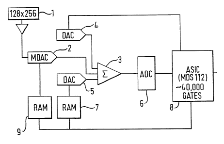
with analogue preprocessing. Figure 1 shows one such architecture for uncooled
detector systems. The output from the detector 1 is first corrected for
response via a
multiplying digital to analogue converter (MDAC) 2. This is achieved by
exposing the
detector, normally during manufacture, uniformly at two levels, one of which
may be
"dark" or chopper, and obtaining from this a multiplication factor for each
element by
which subsequent values received by the element must be multiplied by MDAC 2
to
correct for non-uniformities in response. These multiplication factors are
stored in
random access memory (RAM) 9. The corrected output value for each element is
conveyed to summing amplifier 3, where the output of one or more digital to
analogue
converters (DACs) 4, 5 are subtracted from it. The resultant signal is then
digitised, to
the level required for display by the analogue to digital converter (ADC) 6.
The contents of offset RAM 7 are updated while the detector 1 is looking at a
reference
surface, the closed field, and the feedback loop around the DAC 5 and ADC 6
provide
CA 02205851 1997-OS-22
WO 96/17471 PCTlGB95102755
4
stabilisation to drive the input to the ADC 6 to mid range, or zero, during
this period.
This is achieved by digitising the difference between the DAC 5 and MDAC 2,
which
contains the response corrected signal, and adding the resultant to the data
in the offset
RAM 7. Consequently, after the offset RAM 7 has been updated it contains a
digital
equivalent of the detector response during the closed field, with every
location in the
RAM 7 corresponding to a unique element in the detector 1. If the loop gain is
adjusted
to exactly unity, where the LSB of the ADC 6 corresponds to exactly the LSB of
the
offset DAC 5, then any changes in detector offset are exactly nulled on every
update
once the loop has converged. During the open field this offset data is again
fed to the
DAC 5 and hence to the summing amplifier where it is subtracted from the
response
nnrronta~ cicrn~l tn crPnPr~tP tha TTID iloto ~li~ontl<r Ti<:~. ~. .. t4a..
1.e .1:..:,.:.a.7 .. .~ rl....
vvaavvwu uabaaua, w ~,vaavauw wav. sari uuua uuwu~. 1111) Gall 41611 UG
41b'll,lJGtl lislll~' L11G
ADC 6 for subsequent processing such as temporal re-sequencing for
compatibility with
conventional video standards.
A global offset can be added to the signal at the summing amplifier to adjust
the thermal
window being digitised, thus matching the digitiser range to the thermal scene
being
observed. In Figure 1, this global offset is achieved using a DAC 4 to provide
the
adjustment either manually or under the control of some automatic algorithm
integrated
in the custom IC 8.
For a thermal imaging sensor typical resolutions for the MDAC 2 and offset DAC
5 are
12 and 16 bits respectively, whilst the ADC 6 can be restricted to the 8 bits
normally
used for video display systems.
CA 02205851 1997-OS-22
WO 96117471 PCTIGB95/02755
The offset loop is self correcting and changes in offset due to temperature
drift or l/f
noise are automatically corrected every time the offset RAM 7 updates during
the closed
field. During power up, any random data in the offset RAM 7 rapidly converges
to the
correct values due to the operation of the feedback loop. The rate of
convergence to, and
5 subsequent tracking of, the correct offset values is only limited by the
dynamic range of
the ADC 6 which determines the maximum step between successive updates to the
offset
data.
This signal processing algorithm and architecture has been successfully
applied in low
cost thermal imaging sensors based on arrays of 100 x 100 elements.
This approach, although offering the benefits of low cost, volume and power
consumption, also has limitations. In particular, the response correction
stage (the
MDAC) has a limited bandwidth despite consuming a significant proportion of
the total
power of the analogue circuitry. This is particularly problematic when
operating with
larger or faster detector arrays where higher bandwidths are required, and is
generally
overcome by operating multiple analogue processing chains under the
supervision of a
single digital custom integrated circuit.
A
In addition, the relative position of the MDAC, 2, and the offset correction
DAC, 5, in
the processing chain are fixed, since the offset feedback loop must have the
same gain
" for each element in the array tv function properly. If the MDAC was placed
after the
offset correction DAC 5 this loop gain would be different for each element and
would
introduce image artefacts such as smearing. A consequence of this fixed
architecture is
CA 02205851 1997-OS-22
WO 96/17471 PG"TIGB95102755
6
that the responsivity correction MDAC 2 compounds the offset range
significantly, thus
increasing the dynamic range of the offset DAC 5 required.
A further limitation of this approach is the precision of the analogue
processing circuits
required, which are beyond the capability of current analogue ASIC facilities.
Consequently, the analogue processing must be manufactured from commercially
available DACs and MDACs, limiting the degree of integration and
miniaturisation
possible. This restriction limits the minimum costs and volumes achievable,
particularly
for multiple analogue channel systems.
All of these limitations and restrictions clearly reduce the benefits offered
by the
processing architecture over the alternative direct digitisation in the first
place.
Ideally, the response correction would be implemented irr the digital domain,
after the
signal has been digitised, thus eliminating the MDAC from the circuit and
permitting the
response matching function to be integrated with the remaining digital
processing in
ASIC technology. However, the response variations from the detector would then
be
digitised directly which would significantly limit the scene temperature range
for which
the system would function. This is shown schematically in Figure 2, where the
input to
the ADC is plotted against temperature. The offset correction loop maintains
the input
to the ADC at zero during the closed field as before, but without the MDAC in
the
circuit, the response variations remain uncorrected. Consequently, when
viewing the
infra-red scene, the input to the ADC can be dominated by response variations.
Typical
response variations of ~50% can be present in large arrays of detectors, and
elements
CA 02205851 1997-OS-22
WO 96117471 PCT/GB95/02755
7
close to the extreme response ranges saturate the ADC even for small
temperature
differences from the chopper or reference. The operating range of a system
with
response variations of ~50% is shown in Figure 2 by the dotted box (A).
J
If more extreme temperatures are viewed using a global offset control such as
the DAC
4 in Figure 1, the problem becomes more acute. The output of the DAC
effectively
shifts the input voltage range of the ADC permitting more extreme voltages,
and thus
temperatures, to be digitised. Under such circumstances, extreme response
elements
saturate the ADC and, as the temperature difference from the chopper or
reference
increases, the outputs of fewer and fewer elements can be digitised. This is
shown in
Figure 2 where the offset adjustment results in an ADC input range where
saturation of
some elements always occurs. For temperatures less than T 2 the lowest
response
elements saturate negatively, whilst for temperatures greater than T I the
high response
elements saturate positively. For temperatures between T', and TZ all
elements, except
those very close to the normalised response, saturate the ADC input.
Hence the responsivity matching must be performed prior to the analogue to
digital
conversion if saturation problems are to be avoided, and this limitation has
prevented the
response correction being implemented digitally, despite the potential
benefits.
EP 0138579 partially addresses the problem of a limited resolution of an A to
D
converter by adopting a system in which dark field values are subtracted from
open field
values prior to conversion by the A to D converter. However the resolution
available to
the open filed can still not exceed the resolution of the A to D converter.
The present
invention aims to overcome this limitation and permit the benefits already
mentioned,
CA 02205851 2004-09-03
8
together with additional functions, to be realised.
SUMMARY OF THE INVENTION
EP-0 554 802 discloses a system wherein the output of the A-to-D converter is
fed back to a
summing amplifier at the input of the A-to-D converter such as to compensate
for non
S linearity in a detector element by subtracting the average value of adjacent
elements from the
output of that element. US 4 628 352 discloses a system where non-uniformity
in a closed
field response between different detector elements is compensated for prior to
A-to-D
conversion of the signal and subsequent processing. GB 2 195 855 discloses a
system
wherein an ambient energy pattern is subtracted from the open field signal
prior to the open
field signal being converted to a digital signal. With all these systems, the
A-to-D converter
has to be set to a range sufficient to transmit signals of minimum and maximum
intensity
received.
In accordance with one aspect of the present invention there is provided
signal processing
apparatus for receiving an analogue signal conveying output values of elements
of a detector,
1 S said detector comprising an array of elements, the apparatus comprising:
(a) an analogue to
digital converter for receiving a signal derived from the output values of the
detector
elements; (b) digital processing means for: ( 1 ) receiving a digital output
signal from the
analogue to digital converter; (2) for each detector element, summing
successive values
representative of a viewed scene and derived from the output signal of the
analogue to digital
converter; (3) generating an output signal conveying the sum values for each
detector
element; and (4) correcting for linear and/or higher order non-uniformities in
the response of
each detector element; (c) a memory for receiving and storing digital values
representative of
the sum values; (d) a digital to analogue converter for converting the digital
values contained
in the memory to an analogue signal; and (e) analogue signal modifying means
for
subtracting the analogue signal output by the digital to analogue converter
from the analogue
signal conveying output values of the elements of the detector, such that the
sum value
associated with a particular detector element is subtracted from the
corresponding detector
output value prior to the signal being transmitted to the analogue to digital
converter
In accordance with another aspect of the present invention there is provided a
method of
processing an analogue signal conveying the output values of an array of
sensor elements in a
detector, the method comprising the steps of: modifying the analogue signal to
correct for any
non-uniformity in an offset response of the elements; converting the modified
signal to a
CA 02205851 2004-09-03
9
digital signal using a converter having a relatively low resolution; and
further processing the
signal to correct for linear and/or higher-order non-uniformities in the
response of the
elements; wherein the step of modifying the analogue signal further comprises
the steps of:
tracking the values output from the converter corresponding to the output
values of particular
elements of the detector; and modifying the analogue signal so as to tend to
maintain the
signal applied to the converter within the range of the converter and thereby
determining the
signal output by each element in the array to a higher resolution than that of
the converter.
By employing the present invention it is no longer necessary to employ the
MDAC of
Figure 1, as correction of non-uniformities in linear and higher order
responses can be
achieved in the digital processor. Furthermore the invention enables closed
and open field
values to be "tracked" and subtracted from the input of the A-to-D converter
such that the
resolution of the apparatus is not limited by the resolution of the A-to-D
converter. This
offers considerable savings on both the cost of high resolution A-to-D
converters and also on
power consumption of such converters. The summing circuit effectively now only
determines
for each element the change between successive open fields and successive
closed fields, the
difference between closed and open fields being determined by the digital
processing means.
Preferably, the analogue to digital converter has a resolution less than the
detector and the
digital processing means tracks successive values corresponding to a
particular element and
controls the analogue processing means such as to tend to maintain the signal
applied to the
converter within the range of the converter such that the signal output by
each element in the
array can be determined by the digital processing means to a greater
resolution than that of
the converter. Advantageously the signal from the
1 CA 02205851 1997-OS-22
array is received far both open and closed fields and the digital processing
means tracks
successive values relating to the intensity of any one element for both open
and closed
fields. This enables the resolution for both the closed and open fields to be
far greater
than that of the analogue to digital converter.
5
With some detectors it is not always required to have a closed field between
subsequent
frame readouts, in which case the "closed" field values may be obtained only
once on
manufacture or may be re-set periodically, for example at commencement of
operation
of an imager. Alternatively, several closed fields can be obtained between
each open
10 field.
The invention is particularly advantageous when employed in an imager having a
detector and means for interrupting radiation incident on the detector, each
element of
the detector being read in both a closed field when radiation is interrupted,
and in open
field when radiation is incident on the detector.
For some uncooled infra-red detectors the IDP process is more complicated than
the
simple subtraction of closed field from open field signals. For example a 3
point IDP
process may be required where half the preceding and half the succeeding
closed fields
are subtracted from the open field. This algorithm is particularly simple to
implement
with the present invention since the term to be subtracted from the open field
data can
readily be calculated during the update of the subsequent closed field. The
original
architecture of Figure 1 required the 2 point IDP signal, produced during the
open field
by the summing amplifier, to be stored in an additional block of RAM and
converted to
a;~»=>>:~L~ ~. ,~~r
1 CA 02205851 1997-OS-22
11
3 point IDP data when the subsequent closed field occurred. This additional
field
storage R.AM is not required with the present invention since the open and
closed field
data are stored separately.
~ In addition to the IDP and response matching functions, global offset and
gain
adjustments can also be implemented digitally, thus eliminating a further DAC
from the
analogue processing architecture of Figure 1. All of the digital processes can
readily be
integrated into a single digital application specific integrated circuit
(ASIC) device.
This results in a considerable reduction in cost, power consumption and volume
of the
signal processing electronics, yielding a more economical and marketable
system.
Performing the linear and/or higher order responsivity correction digitally,
rather than
in the analogue domain permits the use of higher resolution responsivity
coefficients.
As already mentioned, a typical resolution for the MDAC of Figure 1 is around
12 bits,
limited by available device performance in a sufficient bandwidth. Digital
responsivity
correction can' be implemented to a precision of 16 or more bits, limited only
by the
storage capacity made available. This increased response correction dynamic
range
offers several benefits. Firstly the precision of the response correction
coefficients can
be increased if required, permitting potentially increased uniformity in the
final image,
even for scenes at significantly different temperatures to the reference.
Alternatively,
a wider range of response variations can be tolerated, permitting lower
uniformity
detectors to be used in the system. Consequently the useful detector yield is
increased,
resulting in reduced system costs.
~~ .,_~~;,~-~ c!~~ET
a; i .:~~t~ ,~.
CA 02205851 1997-OS-22
12
A minor limitation of the present invention is that the difference between
sequential
open fields or closed fields cannot be greater than the dynamic range of the
ADC, to
avoid saturation from occurring, i.e. the transient signal handling capability
may be
limited. Such saturation, if it did occur, would be transitory since
subsequent frames
from the detector enable the open or closed field data to converge to the
correct levels,
the number of frames required to achieve this being determined by the ratio of
the
transient change in signal to the dynamic range of the ADC used. Considering
the
practical implementation of the architecture to design an infra-red sensor
with a
sensitivity of 0.1°C, limited by the quantisation noise of, say, an 8
bit ADC, the
maximum change in scene temperature of any element between frames would be
25.6 ° C
to prevent saturation from occurring. Thus, if the imager was panned across a
scene
containing an area 75 ° above the surroundings, the image of that part
of the scene would
require approximately three frames to converge on the final value, and a
further three
frames to return to background Ievel once the hot area of the scene had been
panned
past. The resultant smear would be similar to, but not the same as, the smear
caused by
bright lights across a visible band video camera. In that instance, the smear
decays
gradually, however in this case the smear would terminate sharply once the
feedback
signal to the summing amplifier brought the input signal to ADC within the
range of the
ADC.
This smearing may not be a particular problem for many applications, but could
be
objectionable under some circumstances. One simple solution, reducing, but not
eliminating the problem, would be to increase the resolution and dynamic range
of the
ADC. In the above example, a 10 bit ADC would provide for temperature
transients of
~'r~;!1:-J ~~rr~
CA 02205851 1997-OS-22
13
102.4°C between subsequent frames- suitable for most thermal imaging
applications
without saturation defects occurring.
Alternatively or in addition to the increased resolution ADC, the update of
the open
and/or closed field digital data can be restricted when the difference between
the two
exceeds the data range being displayed. Thus the open and closed feedback
loops would
not attempt to track signals which caused saturation of both the ADC and the
display,
and would therefore recover more rapidly from saturation when it occurred. The
detection of such saturating conditions is relatively simple using the digital
data for open
and closed fields, the ADC output and the global gain and offset adjustment
data.
Due to the occasional occurrence of such saturation, together with the limited
visual
effect and ease of correction, the restricted transient performance would not
in most
applications be a significant disadvantage.
According to a second aspect of the present invention there is provided a
method of
processing an analogue signal conveying the output values of an array of
sensor
elements in a detector, the method modifying the analogue signal to correct
for any
non-uniformity in the offset response of the elements, converting the modified
signal to
a digital signal, and further processing the signal to correct for linear
and/or higher order
non-uniformities in the response of the elements, the method comprising the
steps of
converting the analogue signal to a digital signal via a converter having a
relatively low
resolution, tracking the values output from the converter relating to the
output values of
particular elements of the detector, and modifying the analogue signal such as
to tend
..,.-,
f~n.W: .~__ ..,~'-1
CA 02205851 2004-09-03
14
to maintain the signal applied to the converter within the range of the
converter thereby
determining to a higher resolution that that of the converter the signal
output by each element
in the array.
BRIEF DESCRIPTION OF THE DRAWINGS
The invention will now be described in detail, in conjunction with the
drawings in
which:
FIG. 1 is a block diagram of a convention processing system;
FIG. 2 is a plot of input to the ADC of the convention processing system
versus
temperature; and
FIG. 3 is a block diagram of an embodiment of a signal processing system
according
to the invention.
DESCRIPTION OF THE INVENTION
One embodiment of the present invention will now be described by way of
example only
with reference to Figure 3 of the accompanying drawings, a schematic diagram
of an imager
incorporating a signal processor in accordance with the present invention.
The imager 10 comprises a 128 x 256 array of sensor elements in a detector 11,
and an
amplifier 12 for amplifying the signal from the detector 11, the output of the
amplifier 12
being fed to the input of summing amplifier 13. The output of the summing
amplifier 13 is
fed to an input of an application specific integrated circuit (ASIC) 14 via 8-
bit analogue to
digital converter (ADC) 15.
The ASIC has associated with it a random access memory (RAM) 16 the function
of which is
discussed below.
Also associated with the ASIC 14 is a video digital to analogue converter
(VDAC) 17 which
converts the time resequenced data, after correction for linear and higher
order 20 non-
uniformities, into a conventional video format analogue signal.
The ASIC 14 is also connected to a RAM 18, the ASIC setting the values in the
storage array
of the RAM, each cell of which corresponds to an element of the detector. The
RAM has two
sections, 18A, 18B, and stores open field and closed field values in the
CA 02205851 1997-OS-22
two respective portions. These values are fed to the summing amplifier 13 via
digital
to analogue converter (DAC) I9, the summing amplifier for each element
providing an
output signal to the ADC equal to the difference between the value received
from the
amplifier 12 and that stored in RAM 18 for both open and closed fields.
5
In operation the output of each element of the detector for a closed field is
read out. The
value in the corresponding cell of the closed field RAM 18A is subtracted from
the
output signal of the detector and the resultant value digitised by converter
15. The ASIC
receives the digitised value for each element of the detector and sets each
cell of the
10 RAM such that if the next closed field value for each element remained the
same, the
output of the ADC would be at a mid-point of its range. If the initial value
input to the
ADC is outside the range of the ADC then the value stored in the RAM 18
rapidly
converges to the value of the signal from the detector with each closed field
readout
until the output of the summing amplifier comes within the range of the ADC.
The
15 signal applied to the RAM will then track the output of the detector.
The imager 10 functions in exactly the same way in respect of open fields,
storing the
offset to be applied to the surnrning amplifier in the open field portion 18B
of the RAM.
The ASIC, knowing both the closed field and open field values applied to the
RAM and
the, open and closed field received from ADC, computes a value relating to the
intensity
of radiation received by an element of the detector by taking the difference
between the
open and closed field values. Because the intensity of radiation incident on
any one
element of the detector is derived from the difference between closed and open
field
values any non-uniformity in offset response between the elements is
immaterial.
CA 02205851 1997-OS-22
16
However, linear and/or higher order non-uniformity in response is not
compensated for
in this manner. This has to be corrected by uniformly exposing all the
elements to two
different intensities of radiation. For each element the ASIC determines from
the
resultant two values received a constant by which the value of each element
must be
multiplied to correct for linear variations in response. This is stored in RAM
16 and
applied to subsequent values received by the ASIC. Higher order non-
uniformities can
be corrected in a similar manner.