Note: Descriptions are shown in the official language in which they were submitted.
CA 02206643 1997-06-02
WO 96117501 PCT/US95I15509
- 1 -
CHEMICALLY GRAFTED ELECTRICAL DEVICES
FIELD OF THE INVENTION
This invention relates to electrical devices and more
particularly to devices employing a chemically grafted
conductive coating.
BACKGROUND OF THE INVENTION
In the fabrication of electronic or electrical devices
and circuits, conductive paths arid contact areas are usually
provided by chemical etching and photolithographic techniques
as in the fabrication of printed circuit boards, and by
plating techniques by which one or more metal layers are
provided such as on electrical contacts or contact areas of
circuit boards, devices and the like. Such fabrication
techniques are well known and are widely employed. They do
however require a number of process steps and specialized
fabrication equipment which adds to the cast and complexity
of the manufacturing process and of the resultant products.
SUMMARY OF THE INVENTION
This invention provides in one aspect an electrical
device having a conductive coating or layer chemically
grafted to a support substrate to produce a durable
conductive surface permanently attached to the underlying
substrate material. The invention can be embodied in an
electrical contact having a contact surface which is part of
a conductive layer chemically grafted to a supporting
substrate. The substrate may be a rigid or flexible single
or multiple layer circuit board, with the grafted contact
areas provided in an intended pattern corresponding to the
pattern of an integrated circuit or other electronic device
or package to be electrically attached to the board. The
' conductive traces of the circuit board can also be grafted
to the substrate. The substrate may also be an element of
' a switch or other electrical or electronic device on which
one or more electrical contacts are farmed by chemical
grafting. In another aspect, the invention is embodied in
an electrical shield or ground plane which may be provided,
CA 02206643 1997-06-02
WO 96/17501 PCT/L1S95/15509
- 2 -
for example, on a circuit board, or other support structure
to provide a shielding enclosure or ground plane. A
shielding gasket or the like can also be provided by the '
invention.
The substrate can be a conductive or non-conductive
material and can be rigid, flexible or resilient to suit the
intended electrical device or circuit requirements. The
conductive layer is composed of a chemically bonded
conductive or non-conductive polymer matrix containing
conductive particles. The conductive particles are each
coated with a polymer material, the polymer coating being
chemically bonded together and to the substrate surface. The
grafted layer may be a single layer of material or two or
more layers of different materials to suit the particular
application.
The polymer coated particles are typically contained
within a slurry which is applied to intended areas of a
supporting substrate surface. The slurry can be applied by
many different techniques including dipping, screen printing,
and spray coating as examples. The applied coating is heated
to dry the coating and to form the chemically bonded
conductive layer on the substrate ~nrface. The conductive
coating may also be applied by other techniques such as
roller coating, brushing, transfer pad printing, ink jet
printing, and atomization spraying.
A layer of homogenous conductive particles can be
provided on the conductive grafted surface to provide a
roughened and hardened surface by which an oxide or other
contaminating layer on a mating electrical contact surface
is penetrated to minimize contact resistance. The
particulate surface contact is the subject of co-pending U. S.
patent application Serial No. 08/349,042, filed December 2,
1994 (attorney docket number AUG-C-556XX).
CA 02206643 1997-06-02
WO 96/17501 PCTI1:JS95/15509
- 3 -
DESCRIPTION OF THE DRAWINGS
Figs. la and lb illustrate one embodiment in which a
' grafted electrical terminal pin embodying the invention is
inserted and retained in a conductive opening;
' 5 Fig. 2 illustrates an embodiment in which a resilient
annular ring wall according to the invEntion provides contact
with an electrical lead inserted through the ring;
Fig. 3 illustrates a controlled impedance contact made
according to the invention;
Fig. 4 shows a printed circuit board utilizing the
invention;
Fig. 5 is a sectional view taken along lines 5-5 of Fig.
4;
Fig. 6 shows a flexible circuit board made according to
the invention;
Fig. 7 shows a board-to-board connector employing the
invention;
Fig. 7a is a partial elevation view of one form of
contact structure for the connector of Fig. 7;
Fig. 8 shows an edge card connector fabricated according
to the invention;
Figs. 9a through 9d show respective views of a terminal
pin interconnect embodying the invention;
Fig. 10 shows a test probe embodying the invention;
Figs. 11a and 11b illustrate an elastomeric interconnect
embodying the invention;
Figs. 12a through 12d illustrate electrical switch
devices employing the invention;
Fig. 13 illustrates an acoustic wave or microwave device
embodying the invention;
Fig. 14 illustrates a metallized diaphragm made
according to the invention;
Fig. 15 illustrates an electrically shielded enclosure
embodying the invention; and
Fig. 16 diagrammatically illustrates one fabrication
method according to the invention.
CA 02206643 2000-06-13
-4-
DETAILED DESCRIPTION
In the foregoing examples, a conductive area or surface
is provided by chemical grafting onto a substrate surface.
The grafting technique is described in an article entitled
"Grafting of Polymer by Purely Chemical Means", Polymer News,
Volume II, No. 11/12, pp. 19-25.
The conductive material to be grafted to the substrate
is composed of conductive particles, such as silver or other
metal, each coated with a conductive or non-conductive polymer
material. The particles are, in one preferred embodiment,
contained within a slurry or other vehicle by which the
particles are applied to a substrate surface. For example,
the slurry containing the particles can be screen printed or
sprayed onto a substrate to form intended conductive areas.
The applied material is heated at a temperature and for a time
sufficient to drive off the liquid vehicle and to cause the
particles to be chemically bonded together and to be
chemically bonded to the substrate surface. Optionally, a
metal such as copper can be plated to the grafted layer, such
as by electroless plating. The conductive particles are
sufficiently proximate to each other to provide a layer of
intended conductivity. When a non-conductive polymer coating
is employed over the conductive particles, the coating is
sufficiently thin and has sufficiently low resistivity to
provide conduction between the closely packed conductive
particles in the polymer matrix to yield an intended level of
conductivity for the grafted layer. The level of conductivity
of the grafted layer is usually higher when a conductive
polymer is employed.
The particles can also be extruded or otherwise formed
into a homogeneous conductive material as illustrated in Fig.
16. The conductive particles are supplied to an extrusion
machine which produces a homogeneous extrusion of material in
an intended shape.
CA 02206643 1997-06-02
WO 96/17501 PCTlUS95/15509
- 5 --
The conductive layer typically has a thickness in the
range of about 0.1 mil to about 2 mils. The particle coating
typically has a thickness of about 10 to 50 Angstroms for
non-conductive coatings, and about 10 to 250 Angstroms for
conductive coatings. The conductivity of the uncoated
particles is typically in the range of about 50 to 104
percent IACS. The conductivity of the coated particles are
typically in the range of 20 to 60 percent TACS for non-
conductive particle coatings, and about 60 to 110 percent
to IACS for conductive particle coatings.
Examples are given below of electrical devices having
one or more conductive areas composed of chemically grafted
coatings.
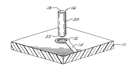
Referring to Figs. la and lb, there is shown a printed
circuit board 10 having a plated through. hole 12 which is
electrically connected to one or more circuit traces 14
provided on or within the circuit board in known fashion.
Electrical connection is made to the plated through hole by
means of a pin 16 composed of a core 18 of thermosetting
material having a conductive layer 20 grafted to the
cylindrical surface and rounded end 22 of the pin 16. The
pin in its initial condition is sized to be inserted into the
plated hole after which exposure to heat causes the core 18
of the pin to expand sufficiently to form a gas tight seal
between the grafted conductive surface 20 and surrounding
plating material of the through hole. The thermosetting
material after its expansion due to heating remains in the
expanded state and thereby provides a permanent gas tight
seal . The pin 16 can be alternatively conf figured to mate
with other electrical contact elements with which a permanent
electrical connection is to be made.
' Referring to Fig. 2, there is shown a grafted annular
ring 30 which is connected to a circuit trace 32 of a printed
' circuit board 34. The ring is aligned around a hole through
the circuit board and into which a lead of an electrical or
electronic device is inserted. The grafted ring is composed
of a resilient core of material such as silicon rubber,
CA 02206643 1997-06-02
WO 96/17501 PCT/US95/15509
- 6 -
having a chemically grafted flexible conductive material on
the surfaces of the core. The opening through the annular
ring is slightly smaller than the diameter of the electrical
lead or pin to be inserted therethrough such that compressive
force is provided between the inserted lead and surrounding
ring to maintain the lead in position. An array of resilient
rings can be provided in a pattern corresponding to the lead
pattern of a device to be connected to the circuit board.
The conductive coating is sufficiently flexible and
resilient to not impeded the resilience of the core material.
The ring can compress when in contact with a mating
electrical lead and expand when out of mating contact without
peeling or cracking of the conductive coating on the surface
of the ring.
The resilient interconnect ring can be fabricated by
molding the core material in the desired shape. A
metallization is applied to the ring surfaces preferably by
chemical grafting, and the particulate layer is then applied
to the surface of the metallization layer. Copper or other
metal may optionally be electroless plated onto the
metallization layer prior to application of the particulate
layer.
Referring to Fig. 3 , there is shown a conductive element
40 having a signal contact 42 engaged with a signal pad 44
~ of a circuit board 46, and a ground contact 48 engaged to a
ground pad 50 of the circuit board. The conductive element
is typically formed of a contact material such as phosphor
bronze or beryllium copper. An insulating layer 51 is
disposed along a portion of the contact element and over
which a conductive layer 53 is grafted to provide a ground
plane. The contact structure thus formed has a controlled
electrical impedence defined by the dimensions and materials
employed.
Figs. 4 and 5 show a multilayer printed circuit board
60 having three inner conductive patterns 62 for providing
an intended circuit configuration, one of the circuit
patterns being electrically connected to a conductive via 64
CA 02206643 1997-06-02
WO 96!17501 PCTlUS95115509
_ ? _
or through hole as shown. An array of conductive contacts
66 is provided on one surface of the circuit board. A
pattern of circuit traces can also be formed on one or both
outer board surfaces. All of the conductive elements of the
multilayer board can be provided by chemical grafting.
Alternatively, some conductive elements can be formed by
other means while some of the conductive elements are formed
by grafting.
Fig. 6 illustrates a flexible circuit board 70 having
an array of parallel traces 72 and contact areas 74 formed
by grafting on a surface of the flexible substrate. Similar
circuit traces and/or contact areas can be provided on the
opposite flexible board surface, as well as in buried layers
within a multilayer board structure.
A further embodiment is illustrated in Fig. 7 which
shows a right angle board to board connector which includes
a connector body 80 of a suitable insulating material, having
on a first face 82 a plurality of conductive contact areas
84 arranged in an intended pattern, and electrically
connected via conductive traces 86 to corresponding contact
areas 88 provided on an orthogonal face 90 of the body. In
use, the contact areas 84 are mated to corresponding contact
areas of printed circuit board 100, and contact areas 88 are
mated to corresponding contact areas of printed circuit board
~ 102. The interconnection assembly of the two circuit boards
and connector body is maintained by a suitable mechanism (not
shown), and is known in the connector art.
The contact areas and traces are chemically grafted to
the underlying surfaces of the body. The surfaces of the
body on which the contact areas are formed may have raised
pedestal areas and which may have a resilient layer on which
the conductive layer is provided. Referring to Fig. 7a, a
conductive layer 81 is grafted to a resilient layer 83 on the
raised pedestal 85. The conductive layer 81 is in electrical
interconnection with the respective traces 87. The connector
body 80 may alternatively be of a resilient or elastomeric
material which is compressed during engagement of the contact
CA 02206643 1997-06-02
WO 96/17501 PCT/US95/15509
_ g
areas with the associated circuit boards to provide contact
pressure. Alternatively, the contact areas and corresponding
traces can be provided on a resilient sheet which is
supported on a rigid material.
Referring to Fig. 8, an edge card connector is shown
which comprises a body 110 of elastomeric material having a
plurality of raised ridges 112 onto each of which a grafted
conductor 114 is provided. The conductors extend down
respective sides of the body as illustrated and through
openings in the bottom portion of the body and thence along
the bottom surface of the body. A circuit board or circuit
card having contact areas corresponding to the contact areas
of the connector is inserted into the connector body for
engagement with the respective contact areas 115 of the
connector. The illustrated edge card connector has
connectors on opposite sides to engage opposite rows of
cantact areas of a double sided circuit board or card. It
will be recognized that single sided connectors can also be
provided by the invention to engage and make contact with
single sided circuit cards. Various other connector
configurations are also contemplated to accommodate various
electrical and electronic interconnect applications and
configurations .
Another embodiment is illustrated in Figs. 9a through
9d wherein grafted conductive areas are provided within
openings of a female socket or interconnect. The
interconnect body 120 has a plurality of holes 122
therethrough each of which has grafted conductive surfaces
124 for electrical contact of corresponding electrical pins
12F of a mating connector 128. Each of the conductive areas
of the interconnect openings terminate on the back surface
in an annular contact area 130 for mating with appropriate '
circuit board or other interconnections. Each of the
connector openings can have an outwardly flared entry section
132 which is also has the conductive coating.
Referring to Fig. 10, there is shown an electrical test
probe having a probe body 140 with an elastomeric spherical
CA 02206643 1997-06-02
WO 96!17501 PCTlUS95l15509
_ g _
probe tip 142 secured at one end. The tip is an elastomeric
ball having a grafted conductive surface. The probe body has
_ a conductive surface or may be of conductive material such
as metal. The probe body is retained within a suitable
fixture to position the tip over the contact area and to
compress the tip against the contact area for electrical
engagement therewith.
The elastomeric spheres with grafted conductive surfaces
can also be embodied in an interconnection device as shown
in Figs. lia and ilb. The spheres 150 are retained within
a suitable housing (not shown) which is interposed between
a printed circuit board 152 having conductive pads 154 and
an electronic device 156 also having conductive pads 158.
The device is forced toward the printed circuit board against
the biasing of the elastomeric spheres and the pad areas of
the device and circuit board are interconnected by the
interposed conductive spheres. The device is maintained in
contact engagement with the circuit board by a suitable
socket mechanism (not shown).
2o The invention can also be usefully employed in the
fabrication of electrical switches, such as shown in Figs.
12a through 12d. In each of these switches, a conductive
contact area is grafted to the actuator which is of a plastic
or other non-conductive material. The electrical terminals
. on the switch housing can be of conventional stamped metal
construction and these terminals have contact areas which are
selectively engaged upon actuation of the switch actuator to
provide switch closure or opening depending on particular
switch contact configuration. Alternatively, the switch
terminals provided on the case can be chemically grafted.
A pushbutton switch is shown in Fig. 12a in which a grafted
conductive contact area 160 is provided on the actuator 162.
Upon manual depression of the actuator, the contact area
engages the confronting contact areas 164 of the switch
terminals. It will be appreciated that various switch
configurations can be provided to provide intended switch
operation. A slide switch is shown in Fig. 12b in which the
CA 02206643 1997-06-02
WO 96/17501 PCT/US95/15509
- 10 -
slidable actuator 166 includes grafted contact areas 167 on
respective ends. A toggle switch is depicted in Fig. 12c in
which the toggle mechanism 168 includes grafted contact areas .
170. Fig. 12d illustrates a switch case or housing having
grafted conductive paths which provide electrical terminals
and contact areas of the switch. In the structure of Fig.
12d, the grafted terminals 171 can be made by a multiple
molding process. Plastic posts have a conductive coating
grafted thereon, and these posts are then molded to the
plastic housing 173 to which grafted contact areas 175 are
provided as illustrated in electrical connection with the
grafted terminals. The terminals 175 are selectively
interconnected by a conductive strip 177 which is actuated
by toggle mechanism 179.
The invention can also be embodied in a surface wave
device as shown in Fig. I3, such as for surface acoustic wave
or microwave applications. A substrate typically of alumina
has formed thereon a pattern of one or more materials
suitable for propagation of an acoustic wave or microwave.
For acoustic wave purposes, the pattern is typically formed
of antimony and bismuth, both of which are deposited and
chemically grafted to the ceramic substrate.
A further embodiment is shown in Fig. 14 wherein a
conc'luctive pattern 181 is provided by chemical grafting on
a non-conductive substrate surface which in the illustrated
embodiment is of dome shape. The diaphragm is sensitive to
an intended characteristic such as heat, vibration or
pressure and to deflect or deform to cause relative movement
of the conductive traces of the pattern 181 to produce an
electrically sensible signal change.
Fig. 15 shows an enclosure or case for an electronic
circuit board, the enclosure having electrical shielding
layers provided on the inner surfaces by chemical grafting
to the two halves of the case or enclosure. The case is
typically formed in two halves 200 and 202 such as by plastic
molding, and is configured to retain a circuit board 204
therein. A conductive coating 206 is grafted to the inside
CA 02206643 1997-06-02
WO 96/17501 PCTIC1S95115509
- 11 -
surfaces of the case to provide RFI and/or EMI shielding.
The shield coating is applied to the inside surfaces of the
case typically by screening and subsequent heating to
catalyze the coating and provide the grafted layer. T h a
W 5 invention is not to be limited by what has been particularly
shown and described, as alternative implementations will
occur to those skilled in the art without departing from the
true scope of the invention.