Note: Descriptions are shown in the official language in which they were submitted.
CA 02213590 1997-08-21
CWC - 144
-1-
FLEXIBLE CIRCUIT CONNECTOR
AND METHOD OF MAKING SAME
BACKGROUND OF THE INVENTION
Technical Field of the Invention
The present invention relates to an electronic flexible circuit
connector and, in particular, to a flexible circuit connector formed through
s a single layer of flexible polymeric film substrate without the use of
solder
to mechanically fasten and electrically connect a male connector to the
substrate.
DESCRIPTION OF RELATED ART
A flexible circuit includes a flexible dielectric substrate having
io conductive inks printed on the substrate surface to define circuit traces.
The dielectric substrate typically comprises a polymeric film and in
particular a polyimide film. Components are attached to be flexible circuit
with component connectors either passing through apertures in the flexible
circuit or being seated on land pads etched into the substrate. The
is electrical contacts of these components are typically soldered in
electrical
contact with the aperture or the land to mechanically secure the component
to the flexible circuit.
CA 02213590 1997-08-21
- 2 - CWC - 144
The characteristics of the dielectric substrate permit a flexible
bending of the substrate to accommodate locating the flexible circuit in
applications where a non-rigid printed circuit is required. However, care
must be taken in shaping the dielectric film or the production of any holes
s through the material since any irregularities in the edges of the dielectric
film can easily lead to tearing of the flexible circuit damaging the circuit
beyond repair. Consequently, connections made with the circuit traces to
interface devices operating with the flexible circuit are typically made by
running the traces to an edge surface of the flexible connector and
io attaching a ribbon connector to the traces by soldering leads in the ribbon
connector to the traces. This is a factor to be considered when creating a
circuit trace layout design for the flexible circuit. The ribbon connectors
typically have a pin socket at the other end for attachment to the interface
device.
is While the use of through hole connection of terminals to dielectric
substrates has been achieved with printed circuit boards, it should be
understood that these printed circuits typically comprise several layers of
polyimide film separated by layers of insulation resulting in a rigid
substrate having a thickness in the order of 0.062 thousands of an inch.
ao One such through hole connector is disclosed in U. S. patent 5,172,472
issued December 22, 1992 to Linder et al. where a multi-layer rigid printed
circuit board fabrication method is disclosed. In this patent, a hexagonal
shaped pin is forced through several layers of a mylar film material having
intermittent insulation layers and a printed circuit core or substrate. The
2s hexagonal shaped pin has a diameter greater than the diameter of the
layers of mylar material and equal to the diameter of the core of the printed
circuit core. As the pin is forced through the openings, its cuts and
deforms the flexible mylar layers into wiping contact with the pin. In order
to cut into the mylar layers without tearing the layers, the rigid core and
CA 02213590 1997-08-21
-3- CWC-144
intermittent layers of insulation between the mylar layers are required,
otherwise it would not be probable to obtain a wiping electrical contact.
U.S. patent 5,548,488 issued August 20,1996 to Scott Hansen
discloses use of an electrical lamp socket mounted to a rigid substrate with
s a flexible circuit sandwiched between the socket and the rigid substrate.
The flexible circuit carnes electrical traces having conductive terminals
with central apertures formed having a slightly smaller diameter than
corresponding aligned apertures in the rigid supporting substrate. The
lamp socket includes two elongate terminal pins which pass through the
io aligned apertures of the flexible circuit and the rigid substrate to deform
the aperture of the flexible circuit against the rigid substrate. Mechanical
fastening of the lamp socket component is made between the terminal pins
of the lamp socket component and rigid substrate. Due to the sensitivity of
the dielectric flexible substrate to tearing, the supporting substrate is
is necessary in order to mechanically secure the terminal pins and two
prevent tearing of the flexible circuit.
There is a need to develop a direct connection of a terminal to a
flexible circuit that does not require a solder paste to mechanically secure
the terminal to the flexible circuit, ensures good electrical contact with the
zo circuit and allows for increased circuit trace design flexibility over the
use
of ribbon connectors.
SUMMARY OF THE INVENTION
The present invention relates to a method for interconnecting a
terminal pin or male connector to a single layer of a polymeric dielectric
as filin flexible substrate used in a flexible circuit. The flexible substrate
has
a female connector defined by a pattern smoothly cut from the flexible
substrate having at least one resilient flap normally restricting passage
through the flexible film and deflecting or folding to receive the pin
terminal in wiping engagement therewith. A coating of electrically
CA 02213590 2002-05-30
- 4 - CWC-144
conductive material is located on the flexible substrate having an electrical
contact land area surrounding the pattern and extending over the foldable
flap. When the male terminal or connector is inserted into the female
connector through the flexible film substrate at the pattern, the flap
deflects
s into wiping and mechanical engagement with the male connector to solely
secure the male connector to the substrate in electrical contact with the
electrically conductive material.
In accordance with the method of the present invention, a laser is
used to cut the pattern into the flexible substrate material. By using a
laser,
a smooth non jagged edge for the pattern is achieved. The pattern
preferably results in three or more foldable flaps. Preferred patterns are the
shape of a star resulting in five or six flaps and the shape of an asterisk
resulting in eight flaps. In these latter two preferred patterns, the flaps
resemble pie shaped slices. It is within the realm of the present invention
~ s to have the tips of the pie shaped slices removed so at the flaps restrict
only
a portion of the passage through the female connection. By smoothly
cutting the pattern into the flexible film substrate, the film has no weak
stress points which can result in tears when the male connector is inserted
into the passage. As a result, the resilient flexible characteristic of the
film
z o material used in the dielectric substrate is preserved in the flaps
allowing
the flaps to mechanically and electrically engage the male connector.
In the preferred embodiment of the present application a cylindrical
shaped pin is disclosed. However, it is envisaged that improvements in the
wiping and mechanical engagement between the flap and pin can be
25 achieved by puttering the shape of the pin to correspond to the pattern
laser
cut into the substrate. Thus, triangular, square or other shaped pin
connectors can be used that correspond to the pattern cut into the substrate.
CA 02213590 1997-08-21
-5- CWC- 144
In accordance with one aspect of the present invention there is
provided a method of manufacturing a female electrical connector in a
single layer of a flexible polymeric film substrate of a flexible circuit
ready
for mechanically securing a male connector directly to the film substrate in
s electrical contacting relation with a circuit trace. The method comprises
the steps of:
directing a laser beam towards the flexible polymeric film substrate
to cut a smooth pattern through the film substrate defining at least one
resilient foldable flap normally restricting passage through the flexible film
io and adapted to deflect to receive the male connector in wiping engagement
therewith; and,
coating an electrically conductive material on the substrate including
a circuit trace having an electrical contact land area surrounding the
pattern and extending over the foldable flap.
is In accordance with another aspect of the present invention there is
provided a female electrical connector for a single layer of a flexible
polymeric film substrate of a flexible circuit ready for mechanically
securing a male connector directly to the film substrate in electrical
contacting relation with a circuit trace. The female connector comprises a
zo pattern smoothly cut through the film substrate defining at least one
resilient foldable flap normally restricting passage through the flexible film
at the pattern. The at least one foldable flap is adapted to deflect when
receiving the male connector in wiping engagement therewith. The female
connector further includes a coating of an electrically conductive material
as on the substrate providing the circuit trace. The coating has an electrical
contact land area surrounding the pattern and extending over the foldable
flap.
BRIEF DESCRIPTION OF THE DRAWINGS
CA 02213590 1997-08-21
-6- CWC- 144
A more complete understanding of the method and apparatus of the
present invention may be obtained by reference to the following detailed
description when taken in conjunction with the accompanying drawings
wherein:
s Figure 1 illustrates the laser pattern cutting step of the present
invention;
Figure 2a, 2b, 2c, and 2d represent different patterns that can be cut
into the flexible dielectric substrate;
Figure 3 is a plan view of a flexible dielectric substrate with circuit
io traces; and,
Figures 4 and 5 are perspective views showing the connection
through the traces and flexible dielectric substrate.
DETAILED DESCRIPTION OF EMBODIMENTS
Referring to the drawings the preferred embodiments of the present
is invention are described. Throughout the description of the preferred
embodiments, reference will be made to cutting of the polyimide material
by the use of a C02 laser. It should be understood that a YAG laser may
be used however because the polyimide substrate lends itself to being
readily cut by low powered lasers, it is more economical to use a C02
ao laser which cost is in the order of magnitude less expensive than a YAG
laser.
While the preferred embodiments of the present invention are
described with respect to a flexible polyimide film substrate, alternative
polymeric materials, such as, for example, some polyesters having
as characteristics similar polyimide film used in the present invention may be
employed for the substrate of the present invention. Preferably, the
substrate of the present invention is a flexible polyimide film having a
thickness typically in the order of 0.002 to 0.012 inches. A suitable
CA 02213590 1997-08-21
-7- CWC-144
polyimide film is that sold on the market by DuPont under the trade-marks
KAPTON~ and CIRLEX~. KAPTON is used for thicknesses below
0.007 inches and CIRLEX is used for thicknesses above 0.007 inches.
The thickness of the polymide film used is proportional to the size of the
s male connector.
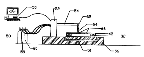
Referring to Figure l, there is shown a laser 52 used to smoothly cut
the patterns 66 in the flexible polyimide film substrate 42. The substrate
42 is mounted to a frame 32 and the co-ordinates of the patterns to be cut
into the polyimide substrate are fed from computer 50 which controls the
io operation of C02 laser 52 and the positioning of computer numerically
controlled (CNC) table 51 mounted relative to platform 56.
CNC tables are known in the industry and the schematic
representation of the table should be provide a sufficient understanding of
the method of making cutting a pattern into the substrate 42. The COZ
Is laser 52 is mounted upon a table or platform 56 and has a helium tank 58,
nitrogen tank 59 and C02 tank 60. The COZ laser 52 generates from its
laser head 62 a focal beam 64 which cuts into and through the polyimide
film 42. The computer 50 controls the laser beam pulse duration, laser
beam power, laser pulsing rate, and gas pressure of gas emitted against the
ao surface of the polyimide film 42 where the laser cuts through the film 42.
The CNC table typically moves at a speed considerably slower than the
pulse rate of the laser beam and hence the speed of movement of the CNC
table relative to the pulse rate is not a significant factor. The distance
between the laser head 62 and the substrate polyimide film 42 is
zs maintained constant by a mechanical and optical sensing system (not
shown) working in conjunction with the computer 50. This maintains the
beam power level at an average power level to the area of the polyimide
sheet irradiated by the beam as the beam moves across the sheet. As the
beam cuts through the film 42 the beam burns a smooth edge along the
CA 02213590 1997-08-21
-8- CWC-144
pattern cut. Consequently, there are no small tears or stress points along
the pattern cut in the film 42 which could tear when direct mechanical
force is applied to the pattern cut.
Referring to Figure 2a, the pattern 70 cut into the substrate 42 is in
s the form of an asterisk with six legs 72 cut through the substrate 42. Each
corresponding adjacent legs 72 define a flap 74. While the legs are shown
as single lines, there may be spacing between adjacent flaps 74. In Figure
2a, the flap has a pie shape. In Figure 2b, the pattern 70 is made from a
semi-circular cut 76 defining a tongue shaped flap 78. In Figure 2c, the
io slices 72 cut into the substrate 42 define three flaps 74. In all of these
patterns 70, the flaps 74 and 78 normally line in the same plane as the
flexible substrate 42 restricting passage through the substrate 42. While
the drawings show only one pattern in the substrate, hundreds of patterns
may be cut into the flexible circuit with the centers of the patterns cut
is wittin 0.04 inches. The size of the diameter of the patterns cut into the
flexible substrate 42 may be in the order of 0.03 inches. Hence the use of
a laser to cut these patterns quickly into substrate 42 is a preferred cutting
mechanism.
Figure 2d shows a similar pattern to Figure 2c, however at the
ao center of the cut is provided an open cut aperture 80. In this embodiment,
the flaps 74 normally restrict a portion of the passage to be formed through
substrate 42.
Refernng to Figure 3 substrate 42 is shown having coated thereon
traces 20 of electrically conductive material. These traces may comprise a
zs cold or a copper material. The traces may also comprise a conductive ink.
Traces 20 are coated onto the substrate 42 to define circuit designs in
accordance with the circuit to be implemented by the flexible circuit 22. A
land area 24 includes a pattern 70 below the coating similar to the asterisk
pattern shown in Figure 2a. A portion of the substrate 42 is shown and it
CA 02213590 2002-05-30
- 9 - CWC-144
should be understood at hundreds of traces may be present on the substrate.
The land area 24 together with the pattern 70 cut into the substrate forms the
female connector designated 92.
Referring to Figures 4 and 5, the male connector or pin terminal 90 is
s shown to pass through a portion of the substrate 42. A local portion 42 of
the
substrate is shown for simplicity. As the pin 90 is inserted into the female
connector 92, the pin 92 defects the flexible flaps 74. The resilience of the
flaps 74 cause flaps 74 to wipe against the pin 90 and mechanically hold the
pin 90 in place within the passage 75 defined between the folded flaps 74. The
pre-cut patterns 70 allow for the deflection of the flaps 74 with minimal
force
applied during pin 90 insertion. As better seen in Figure 5, the conductive
land
area 24 follows the fold in flap 74 and engages in electrical contact the pin
90.
Removal of the pin 90 from substrate 42 results in flaps 74 returning to a
position restricting access through, or closing, the passage 75 in the
substrate
42.
Advantage is found with the present invention in that the male
connector pin 90, which is cylindrical in shape, is held solely in mechanical
and electrical engagement with the trace 24 coated on the substrate 42 and the
flaps 74. No other mechanical or chemical fastening is required to maintain
the
z o connector pin 90 in the restricted passage opening within the substrate
42.
While a pin is shown in the Figures, the pin may represent a terminal of a
component or it may represent a terminal connection of wire leading to an
interface device. The shape of the pin may be chosen to correspond to the
pattern cut into substrate. 'The need for using ribbon connectors, which
require
2 5 traces to be run to the edge of the flexible circuit, is reduced by the
use of the
connection of the present invention. Ribbon connectors can still be used with
the flexible circuit, however it now becomes a question of design choice and
optimization as to where connections to the flexible circuit are to be made.
CA 02213590 2002-05-30
-10 - CWC-144
To improve the pin connection with the flaps, the pin connector
preferably has a gold plated tip and the area surrounding the pattern on the
substrate is preferably gold plated.
As can be seen from Figures 4 and 5, as pin 90 passes through
s substrate 42, a portion of the flaps 24 are deflected. This is because the
depth of the edges of the pattern cut into the substrate 42 to form the flaps
74 which is greater than the thickness of the pin 90, also as shown in
Figures 4 and 5. Consequently, the pin 90 causes deflection of flaps 74
without placing any undue stresses on the ends of the pattern cut into the
substrate 42 which could otherwise result in the substrate material tearing.
It should be understood that various alternative embodiments may
be readily apparent to a man skilled in the art in view of the teachings as
set out here and above.