Note: Descriptions are shown in the official language in which they were submitted.
CA 02214586 1997-09-22
-1- 059237:0112
VOLTAGE AND CURRENT HA8ED CONTROL
AND TRIGGERING FOR ISOLATOR SORGE PROTECTOR
FIELD OF THE INVENTION
This invention pertains generally to the field of
electrical systems and apparatus therefor, and more
particularly to devices for blocking the flow of DC current
in such systems while providing AC and fault current
grounding.
HACRGROUND OF THE INVENTION
Isolator surge protectors (ISPs) are electrical
devices that are designed to block the flow of unwanted DC
current in electrical systems while simultaneously allowing
the flow of normal AC current to ground. ISPs also allow
the flow of transient and fault currents to ground. Such
fault currents may be several orders of magnitude higher
than the normal operating currents of the system in which
the ISP is used.
ISPs are used in various high power electrical
system applications. High power transformers are used for
the transmission and distribution of electrical power.
These three phase transformers include a neutral line which
is connected to ground. Unwanted stray DC current can flow
from the ground into the transformer through this neutral
CA 02214586 1997-09-22
to ground connection. Such transformers are not designed
to accommodate a DC current flowing through the transformer
windings. DC currents as low as several amperes can cause
partial core saturation, resulting in excessive power
losses in the transformer (i.e., excessive heating), a drop
in system voltage, the introduction of undesirable
harmonics, and a significant increase in noise level.
Sources of DC current that can cause this problem include
geomagnetically induced current (GIC) caused by solar
flares, stray DC current from rapid transit systems
typically found in large cities, and stray DC current
associated with high-voltage DC transmission systems,
particularly when operating in the monopolar mode (i.e,
earth return mode). Unwanted DC current in the high power
three phase transformer can be blocked by inserting an ISP
between the transformer neutral connection and ground. The
ISP both blocks DC current and simultaneously allows the
flow of normal AC current to ground. The ISP also allows
for the flow of transient fault currents to ground. Such
fault currents can be several orders of magnitude higher
than the normal currents found in the transformer.
ISPs may also be used in association with systems
that protect metal structures against corrosion by the
application of a DC bias voltage. Many metallic structures
and systems are protected against corrosion by cathodic
methods. For example, metallic gas transmission and
distribution lines are protected against corrosion to
prevent gas leaks, particularly in certain environments.
Metal encased high-voltage underground transmission lines,
and the metal hulls of ships, are other examples of
metallic objects which are often cathodically protected.
The most common method of cathodic corrosion
protection of metallic systems is to apply a negative DC
potential to the system to be protected. The negative DC
potential applied to the system will typically be in the
0.6 volt to 3.0 volt range relative to ground. The
cathodically protected system is isolated from ground to
prevent the flow of DC current from the protected system.
While this procedure helps to eliminate corrosion, it
CA 02214586 1997-09-22
-3-
introduces a potential safety problem. Often, the
protected system is an inherent part of an AC power system,
or is coupled to such a power system through resistive,
capacitive, or inductive coupling. In the event of a
fault, e.g., a short circuit, within the power system, or
between the power system and the protected device, the
voltage on the electrically isolated corrosion protected
system may rise to unsafe levels.
To prevent such cathodically protected systems
from reaching unsafe voltage levels in the event of a
fault, lightning, switching transient, or other system
disturbance, it is desirable that the protected system be
- connected to ground through an ISP or similar device. The
ISP presents a high impedance to DC, at least up to the DC
voltage level of interest, but presents a low impedance to
AC at all times so that the voltage level on the corrosion
protected system is limited to values safe for personnel
and equipment.
Another application of ISPs is for the prevention
of stray electrical currents associated with farm
installations, particularly dairying equipment. Such stray
electrical currents can present a significant economic
problem for farm operations. Dairy operations are
susceptible to stray electricity because cows are extremely
sensitive to electricity, much more so that humans, and
will respond to potentials as low as one volt or less. One
solution to such a problem is to insert a blocking device,
such as an ISP, between the primary and secondary neutrals
of the distribution transformers serving the farm. The
blocking device used opens the link between the transformer
neutrals during normal operation, and closes the link very
rapidly anytime the voltage between the neutrals exceeds a
predetermined level. Such an overvoltage might be caused
by a transformer failure, lightning surge, or other surge
condition. For dairy farm applications, the blocking
device will normally be required to block normal AC
currents as well as DC.
CA 02214586 1997-09-22
-4-
Known ISPs typically include a main DC blocking
(or AC bypass) capacitor which prevents the flow of DC
current, while allowing the flow of normal AC currents to
ground. Such ISPs preferably also include a bypass
circuit, which provides a low impedance path across the
capacitor when the voltage across the capacitor exceeds a
predetermined level as a result of an AC or DC fault or
surge condition. High speed electronic switching devices
capable of handling large currents, such as silicon
controlled rectifiers (SCRs), have been used to implement
the low impedance bypass path. However, for applications
in which the ISP is connected to systems which are subject
to an external DC bias, such as cathodically protected
systems, the external DC bias may be greater than the turn-
off voltage of the switching devices employed in the bypass
circuit. Thus, the external DC bias can operate to hold
the electronic switches of the DC blocking device in a
conductive state, thereby maintaining the low impedance
path, and bypassing the DC blocking capacitor, even though
the event which caused the triggering of the switches has
ended. In such a state, the bypass path is stuck in
conduction, with the external DC bias preventing proper
operation of the DC blocking device.
The isolator surge protector described in U.S.
Patent 5,436,786, to Pelly, et al., resolves the problem of
an ISP being stuck in conduction by the presence of a DC
bias voltage. In accordance with Pelly, et al., an ISP
preferably includes an auxiliary bypass path which short
circuits the high current capacity SCRs of the main bypass
path after the triggering event has passed. The auxiliary
bypass path thus shunts the DC current which is maintaining
the SCRs in a conducting state away from the SCRs, such
that the voltage across the SCRs falls below their holding
voltages. Thus, the SCRs will not become permanently stuck
in conduction by the external DC bias.
In high voltage ISP applications,~the energy
stored in the main DC blocking capacitor at the instant
that the switching devices (SCRs) in the bypass circuit are
CA 02214586 1997-09-22
,, , _5_
fired is relatively high. In accordance with Pelly, et
al., an inductor is preferably put in series with the main
DC blocking capacitor to prevent the capacitor from dumping
all of its energy into the SCRs in the bypass circuit
within a short time (a few tens of microseconds) after the
SCRs are triggered. This energy dump may be acceptable at
low voltage levels, where neither the energy stored in the
capacitor, nor the instantaneous SCR voltages, are too
great. At high voltage, however, the rapid dump of a large
amount of energy from the capacitor could damage or destroy
the bypass circuit switching devices. The inductor
prevents an immediate energy dump from the capacitor. It
greatly alleviates the stress on the bypass circuit SCRs by
letting the capacitor dissipate its energy slowly, over a
multiple number of cycles of decaying oscillations. The
ISP control circuitry, which controls triggering of the
SCRs in the bypass circuit, ensures that once the
oscillatory discharge is set in motion (by initially firing
an SCR) the SCRs in the main bypass circuit are kept in
essentially continuous conduction (i.e., without the
instantaneous blocking voltage applied across the bypass
circuit being allowed to rise above a few volts), until the
oscillation has been completed. Thus, after the bypass
circuit switching devices are initially triggered at a high
triggering level, e.g., 300 volts, the ISP controller
establishes a period, e.g.,~ 80 milliseconds, wherein the
bypass circuit switching devices are fired at a much lower
voltage level, e.g., 5 volts, until all of the energy
initially stored in the DC blocking capacitor is
dissipated. Without this feature, the oscillation
resulting from the energy stored in the blocking capacitor
and the series connected inductor would be reflected from
the ISP back to the power system to which the ISP is
connected, rather than being kept as an internal event
within the ISP.
In previously known ISPs of the type described,
continuous operation of the ISP outside of normal rated
operating conditions can cause damage to the ISP's DC
CA 02214586 2004-08-25
-6-
blocking capacitor. If the sum of a steady state external
DC bias voltage applied across the ISP, plus the steady
state peak AC voltage due to the AC current in the DC
blocking capacitor, is higher than the trigger voltage
level of the ISP, the instantaneous voltage across the
capacitor will repeatedly reach the trigger level. This
will cause repeated triggering, and repeated rapid high
current discharge of the DC blocking capacitor through the
bypass circuit SCRs. Continuous operation under such
conditions can cause excessive power dissipation and
possible failure of the DC blocking capacitor.
The less the DC bias voltage applied across an
ISP the more AC voltage can be developed across the DC
blocking capacitor, and the more AC current can flow
through the capacitor, without the voltage across the ISP
itself reaching the trigger voltage level. Thus,
particularly at low values of DC bias voltage, the AC
current through the ISP DC blocking capacitor could exceed
the rms current rating of the capacitor without initiating
triggering of the ISP bypass path. Continuous high AC
current operation of the ISP could cause damage to the DC
blocking capacitor. Previously known ISPs, which provide
triggering of the bypass circuit SCRs based only on the
voltage across the ISP exceeaing a triggering voltage
level, do not provide protection for the DC blocking
capacitor by triggering of the bypass circuit SCRs in the
case where the total AC current rating of the capacitor is
exceeded but the trigger voltage level of the ISP is not
reached.
SUMMARY OF T8E INVENTION
As here described, an isolator surge
protector (ISP) is provided which blocks DC current,
passes AC current, and self-limits the voltage across
it under excessive voltage and current conditions.
The ISP provided is particularly suitable to applications
such as connecting a cathodically protected metal structure
CA 02214586 2004-08-25
_7_
to ground, to provide DC isolation of the structure while
providing for the free flow of AC current, and AC and DC
fault currents, from the structure to ground. Such an ISP
may, however, be employed in any application requiring the
blocking of DC current and the passing of normal AC currents
and AC and DC fault currents.
An ISP here described is controlled to prevent
repeated triggering at a high primary triggering voltage of
the switching devices in the main bypass path under abnormal
high voltage steady state conditions, thereby preventing
repeated rapid high current discharge of the ISP's DC
blocking capacitor. This feature prevents excessive power
dissipation and possible failure of the DC blocking
capacitor under abnormal steady state operating conditions.
The ISP is preferably also controlled such that the main
bypass path switching devices are triggered to prevent
damage to the DC blocking capacitor when the rms AC current
through the capacitor exceeds the current rating of the
capacitor. The ISP preferably also provides a warning
indication that the voltage and/or current applied to the
ISP is beyond the normal operating range, and that
triggering of the bypass path is occurring.
An ISP here described includes a DC blocking
capacitor (AC bypass capacitor) which blocks normal
levels of DC current while allowing the free flow of normal
AC currents. A main bypass path circuit is connected
across the DC blocking capacitor. The main bypass path
includes high power switching devices, such as SCRs, which
are triggered on to provide a low impedance bypass
path across the DC blocking capacitor under fault
conditions. An ISP control and firing circuit provides
primary triggering signals to the main bypass path SCRs
when the voltage across the ISP exceeds a selected
primary voltage trigger level. To prevent overheating of
CA 02214586 2004-08-25
_g_
and damage to the DC blocking capacitor due to repeated
triggering at an abnormally high steady state voltage level
in excess of normal ISP operating conditions, a secondary
triggering period is initiated by the ISP control and
firing circuit immediately following each primary
triggering event at the primary voltage trigger level.
During the secondary triggering period, the ISP control and
firing circuit triggers the SCRs in the main bypass path at
a secondary voltage trigger level across the ISP which is
less than the primary voltage trigger level. The secondary
triggering period is maintained for an extended period of
time, e.g., at least one second, before a new triggering
event is allowed to occur at the primary voltage trigger
level. Institution of the secondary triggering period
prevents repeated retriggering at line frequency at the
high primary voltage trigger level, thereby substantially
reducing the power dissipation of the DC blocking
capacitor.
To protect the DC blocking capacitor from damage
due to excessive AC currents through the capacitor which,
nevertheless, do not cause the primary voltage trigger
level of the ISP to be reached, an ISP described
preferably provides for primary triggering of the SCRs in
the main bypass path under either of two conditions.
First, as described previously, primary
triggering preferably occurs when the total instantaneous
voltage across the ISP reaches a set absolute maximum
value, the primary voltage trigger level. Second, primary
triggering of the bypass path switching devices also
preferably occurs when the current in the DC blocking
capacitor reaches a set maximum level, the primary current
trigger level, whether or not the total instantaneous
voltage across the ISP has reached the primary voltage
trigger level. In either case, whether the initial primary
triggering event is the result of the total instantaneous
voltage across the ISP reaching the primary voltage trigger
level, or the current in the DC blocking capacitor reaching
the primary current trigger level, the primary triggering
CA 02214586 2004-08-25
_g_
event is preferably followed by an extended period of
secondary triggering, as described above, during which
triggering of the SCRs in the main bypass path occurs at a
low secondary voltage trigger level and AC current is,
therefore, essentially diverted from the DC blocking
capacitor into the bypass path SCRs.
An indication is preferably provided whenever primary
triggering occurs. This indication, such as a flashing
LED, provides a warning that the voltage and/or current
applied to the ISP is beyond the normal operating range,
and that triggering of the main bypass path SCRs is
occurring.
After completion of the extended period of
secondary triggering, during which the main bypass path
SCRs are triggered at the low secondary voltage trigger
level, the SCRs in the main bypass path are turned off to
restore the DC blocking capability of the ISP. Due to the
presence of a DC bias voltage in the system of which the
ISP is a part, a DC component of current may have built up
in the main bypass path SCRs during the secondary
triggering period. Therefore, the main bypass path SCRs
can become stuck in conduction with a unidirectional
pulsating current (AC plus DC current). In order to
commutate off the main bypass path SCRs, the ISP preferably
includes an auxiliary bypass path, including an auxiliary
bypass path switching device, such as a MOSFET, which is
switched on briefly by the ISP control and firing circuit
following completion of the secondary triggering period.
Any remaining current in the main bypass path SCRs is thus
diverted through the auxiliary bypass switch, thereby
commutating off the main bypass path SCRs in the event that
they are stuck in conduction.
During the secondary triggering period, DC
current, along with AC current, is allowed to flow through
the main bypass path. Thus, DC energy will become stored
in the inductances associated with the system to which the
ISP is attached, as well as in the internal inductances of
CA 02214586 1997-09-22
-10-
the ISP itself. For example, DC energy may become stored
in the windings of a power transformer and the transmission
system to which the ISP is connected. This stored DC
energy will cause the voltage across the ISP to rise once
the main bypass path SCRs have been turned off, and could
cause a false retriggering at the primary voltage trigger
level. To dissipate this energy, a voltage clamp circuit
is preferably provided which prevents any voltage rise
across the ISP, beyond a certain clamp voltage level,
l0 following completion of the secondary triggering period,
and commutation off of the main bypass path SCRs. The
voltage clamp preferably bypasses the DC current through a
switching device into a resistor, which dissipates the
stored system energy. The voltage clamping period is
preferably allowed to occur for a duration, e.g., one
second, sufficient to dissipate the stored DC energy before
primary triggering of the SCRs in the main bypass path is
reenabled. When the DC component of the current in the ISP
reaches zero, all of the DC energy stored in the system
inductances has been removed. After completion of the
voltage clamping period, operation of the ISP returns to
its original pre-fault state. Primary triggering of the
main bypass path SCRs may then occur due to either the
voltage level across the ISP exceeding the primary voltage
trigger level or the AC current in the DC blocking
capacitor exceeding the primary current trigger level.
Triggering of the main bypass path SCRs, as well
as control of the auxiliary bypass path and the voltage
clamp circuit, is provided by an ISP control and firing
circuit. The ISP control and firing circuit may be
implemented using conventional analog or digital
components, or any combination thereof, and may be a
microprocessor based system. The ISP control and firing
circuit is preferably an autonomous, self-powered, system
that is provided with power for operation during the
primary and secondary triggering periods by energy stored
on a storage capacitor from the voltage applied across the
ISP prior to primary triggering of the main bypass path
CA 02214586 2004-08-25
-11-
SCRs. In some situations, such as where the main bypass
path SCRs are to be triggered due to an AC current through
the DC blocking capacitor which exceeds the primary current
trigger level, the peak AC current at which primary
triggering is required will not produce sufficient peak
voltage across the ISP to provide for operation of the ISP
control and firing circuit. A voltage boosting add-on
circuit may preferably be provided to boost the voltage
level provided to the ISP control and firing circuit
storage capacitor from the voltage level across the ISP
when AC current dependent primary triggering of the main
bypass path SCRs at low voltage levels is required. The
add-on circuit preferably employs a transformer having a
turns ratio such that the boosted voltage level provided to
the ISP control and firing circuit storage capacitor is
sufficient for primary triggering of the main bypass path
SCRs.
An ISP here described also preferably
provides for rapid firing of the main
bypass path SCRs when a fast rising voltage, such as is
caused by a lightning strike, appears across the ISP. For
a fast rising voltages, the ISP control and firing circuit,
which normally initiates primary triggering of the main
bypass path SCRs, cannot react quickly enough to fire the
SCRs to prevent dangerously high voltage levels from
appearing across the ISP. Thus, an auxiliary, virtually
instantaneous, SCR firing mechanism is preferably provided
which limits the peak voltage across the ISP even under
severe lightning strike conditions. Such an auxiliary
firing mechanism may be provided via the use of a zener
diode connected between the anode and gate of each of the
main bypass path SCRs. The zener diodes trigger the main
bypass path SCRs into conduction when the voltage across
the ISP exceeds an auxiliary voltage trigger level such
that the breakover voltage of the zener diodes is exceeded.
The auxiliary voltage trigger level is preferably
sufficiently above the primary voltage trigger level such
that the auxiliary SCR firing mechanism, via the zener
CA 02214586 1997-09-22
-12-
diodes, plays no part in the operation of the ISP when the
SCRs in the main bypass path are fired at normal line
frequencies.
Further objects, features, and advantages of the
present invention will be apparent from the following
detailed description when taken in conjunction with the
accompanying drawings.
BRIEF DEBCRIPTION OF THE DRAWINGB
In the drawings:
Fig. 1 is a schematic circuit diagram of a power
system including an isolator surge protector in accordance
with the present invention, showing one application of the
present invention.
Fig. 2 is a schematic circuit diagram of a known
isolator surge protector.
Fig. 3 is a schematic circuit diagram of an
isolator surge protector in accordance with the present
invention.
Figs. 4-7 are detailed schematic circuit diagrams
of a voltage and current based control and firing circuit
for an isolator surge protector in accordance with the
present invention.
Fig. 8 is a schematic circuit diagram of an
isolator surge protector in accordance with the present
invention including a voltage boosting add-on circuit for
providing a boosted voltage level to the isolator surge
protector control and firing circuit for low voltage
operation thereof.
Fig. 9 is a detailed schematic circuit diagram of
the voltage boosting add-on circuit of Fig. 8.
Figs. 10-12 are waveform diagrams illustrating
the operation of an isolator surge protector in accordance
with the present invention under abnormally high DC voltage
and zero AC voltage operating conditions.
CA 02214586 2004-08-25
-13-
Fig. 13 is a waveform diagram illustrating
various voltage waveforms for an isolator surge protector
control and firing circuit in accordance with the present
invention operating under abnormally high AC current and
zero DC bias voltage operating conditions.
Figs. 14-16 are waveform diagrams illustrating
various voltage waveforms for an isolator surge protector
control and firing circuit in accordance with the present
invention operating under various abnormally high AC
current operating conditions.
Fig. 17 is a wavefortn diagram illustrating
operation of an isolator surge protector control and firing
circuit in accordance with the present invention under
simulated lightning strike conditions.
DETAILED DESCRIPTION OF THE PREFERRED EMBODIMENTS
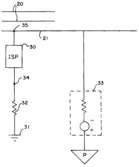
With reference to the drawings, a schematic view
of the interconnection of power system lines 20 and a DC
isolated structure 21 is shown in Fig. 1 for purposes of
illustrating an exemplary application of an isolator surge
protector (ISP) 30 in accordance with the present
invention. The isolated structure 21 may be, for example,
a pipe used in a metal encased high voltage system, a
ground stake, or a gas transmission line. Because of
conducting line resistance, imperfect electrical contact
with the structure 21, and the character of the ground 31,
a certain finite resistance 32 exists between the structure
21 and the true ground potential. An external DC source 33
may be connected to the structure 21 to apply a DC bias
voltage to the structure 21 to cathodically protect the
structure from corrosion by minimizing the oxidation of the
structure 21. The ISP 30 may be connected to the structure
21 at node 35 and the ground 31 at node 34 as illustrated.
The ISP 30 normally presents a very high DC impedance
between nodes 35 and 34, so that substantially no DC
current flows between the nodes. Thus, DC voltages
appearing on the structure 21 are not transmitted through
CA 02214586 1997-09-22
-14-
the ISP 30 to the ground 31. In the event, however, of a
fault on the structure 21, such that voltages above a
selected primary voltage trigger level are applied to the
structure 21, the ISP 30 switches to provide a low
impedance path between the nodes 35 and 34, thereby
shunting any fault current back to the ground 31. For
example, if the power system lines 20 short circuit to the
structure 21, the ISP 30 provides a path to ground 31.
It should be understood that the exemplary
application illustrated in Fig. 1 is only one of many
potential applications for ISPs in accordance with the
present invention. An ISP in accordance with the present
invention may be used in any application requiring the
blocking of DC current and the passing of normal AC
currents and AC and DC fault currents. For example, the
ISP 30 may be connected between the neutral of a wye-
connected three phase power transformer and ground. In
such an application, normal AC current will be allowed to
flow freely through the transformer windings, but stray DC
current, such as geomagnetically induced current (GIC),
will be blocked by the ISP 30 and prevented from flowing
into the transformer. Under fault conditions, the ISP 30
becomes an effective short circuit, allowing free flow of
AC and DC fault currents from the transformer through the
ISP to ground.
A typical prior art ISP is shown in simplified
block diagram form in Fig. 2, and is described herein in
order to illustrate limitations of prior art ISPs which are
remedied by an ISP in accordance with the present
invention. The prior art ISP 40 is illustrated as
connected by ISP terminals 41 and 42 to a structure which
applies a steady state DC voltage level V~ 43 and a steady
state AC current level IAA 44 to the ISP 40. The prior art
ISP 40 includes a main bypass path 46, an auxiliary bypass
switch 48, and a DC blocking capacitor 50 connected in
parallel with each other and in series with an inductor 52
across the terminals 41 and 42 of the ISP 40. The DC
CA 02214586 1997-09-22
-15-
blocking capacitor 50 blocks DC current from passing
between the terminals 41 and 42 of the ISP 40, while
allowing the flow of normal AC operating current through
the ISP 40. The remainder of the ISP circuit 40 only plays
a role under transient or steady state external system
fault conditions. The main bypass path 46 includes
antiparallel connected switching devices, e.g., SCRs, 54
and 56. Zener diodes 58 and 60, along with current
limiting resistors 62 and 64, are connected between the
anodes and gates of each SCR 54 and 56, respectively. The
breakover voltage of the zener diodes 58 and 60 determines
the primary voltage trigger level of the main bypass path
SCRs 54 and 56. Under a fault condition, when the
instantaneous voltage across the ISP, in either polarity,
exceeds the primary voltage triggered level, one of the
SCRs 54 or 56 is triggered into conduction, thereby
creating a low impedance bypass path across the ISP 40.
The low impedance bypass path 46 conducts the AC or DC
fault current safely across the ISP 40. The auxiliary
bypass switch 48 plays no part in the triggering of the
SCRs 54 and 56 in the main bypass path 46. The auxiliary
bypass switch 48 is triggered in response to the voltage
waveform across the ISP to provide a low impedance
auxi~iary bypass path across the ISP 40, after a fault
condition has cleared, to commutate off the main bypass
path SCRs 54 and 56 which may become stuck in conduction
during the fault triggering period due to the presence of
an external DC bias holding the SCRs in a conductive state.
The prior art ISP 40 has several undesirable
limitations when operating under certain conditions that
are outside of the normal rated operating conditions of the
ISP. For example, when the ISP 40 is operating under
abnormal steady state operating conditions wherein the
steady state external DC bias voltage V~, plus the steady
state peak AC voltage due to the AC current IAA in the
bypass capacitor 50, rises higher than the trigger voltage
level of the ISP, the instantaneous voltage across the
CA 02214586 1997-09-22
-16-
blocking capacitor 50 will repeatedly reach the trigger
level, causing repeated triggering of the main bypass path
SCRs 54 and 56 up to twice each cycle. This repeated
triggering causes repeated rapid high current discharge of
the DC blocking capacitor 50 through the main bypass path
SCRs 54 or 56. Continuous operation under these conditions
can cause excessive power dissipation and possible failure
of the blocking capacitor 50. An exemplary and approximate
worse case analysis of the problem follows. Each time the
blocking capacitor 50, with capacitance CAP, discharges from
the trigger voltage level V.Lm~, energy of 1/2 C~PV.~~2 is
dissipated. This energy dissipation is distributed between
the internal resistance of the Uc: blocking capacitor 50,
the external wiring, and the SCRs 54 and 56. Such energy
dissipation could occur twice per cycle, giving an average
power dissipation of 2 x 1/2 C~PV.L~~z x f, where f is the
frequency of the AC current IAA. For a DC blocking
capacitor 40 with a capacitance of CAP=10,000~,F, a trigger
voltage of 12V, and a frequency of 60 Hz, the total average
power dissipated is 86W. For a trigger voltage of 20V, the
total average power dissipation increases to 240W. These
levels of continuous average power dissipation can result
in failure of the DC blocking capacitor 50.
A second limitation of the prior art ISP 40 is
that potentially damaging rms current levels, exceeding the
rms current rating of the DC blocking capacitor 50, can
flow through the capacitor 50 under abnormal steady state
operating conditions, without the triggering voltage level
of the ISP 40 ever being reached, and, therefore, without
the main bypass path SCRs 54 and 56 ever being activated.
The less the DC bias voltage V~ applied across the ISP 40,
the more AC voltage can be developed across the DC blocking
capacitor 50, and the more AC current can flow through the
capacitor 50, without the trigger voltage level of the ISP
40 ever being reached. Thus, at low values of DC bias
voltage, the AC current through the DC blocking capacitor
50 is more likely to exceed the rms current rating of the
CA 02214586 1997-09-22
-17-
capacitor 50. As an example, if the absolute voltage
trigger level of the ISP is 20V, then, with zero DC bias
voltage, a capacitor of 10,000~F would carry an rms current
of 53A at 60 Hz before the 20V trigger level of the ISP 40
is reached. This current level is well above the 30A
rating of the typical preferred 10,000~F capacitor
component used in the ISP 40.
An ISP 70 in accordance with the present
invention, which corrects the undesirable operating
limitations of the prior art ISP 40, is described with
reference to the schematic block diagram of Fig. 3. The
ISP 70 of the present invention includes a main bypass path
72, an ISP control and firing circuit 74, and a DC blocking
capacitor 76 connected in parallel with each other at nodes
A and B of the ISP 70 and in series with an inductor 78
across the terminals 80 and 82 of the ISP 70. Under normal
operating conditions, the main bypass path 72 and the ISP
control and firing circuit 74 provide high impedance
blocking of both AC and DC across the terminals 80 and 82
of the ISP 70. The DC blocking capacitor 76, which may
also be known as, and functions as, an AC bypass capacitor,
blocks DC current from passing between the terminals 80 and
82 of the ISP 70 while allowing the flow of normal AC
operating current across the ISP 70. The remainder of the
ISP circuit 70, including the main bypass path 72, and the
control and firing circuit 74, only plays a role under
abnormal system fault conditions.
The main bypass path 72 includes anti-parallel
connected switching devices 84 and 86 connected between
nodes A and B of the ISP 70. The switching devices 84 and
86 are preferably implemented as power switching devices
capable of handling large fault currents, such as silicon
controlled rectifiers (SCRs). While shown conceptually in
Fig. 3 as single SCRs 84 and 86, for high power
applications it is preferable to implement the main bypass
path 72 using multiple pairs of SCRs 84 and 86 connected in
parallel with each other. Multiple parallel SCR pairs are
employed to increase the current handling capability of the
CA 02214586 1997-09-22
-18-
ISP 70. With multiple paralleled SCRs, high fault currents
can be divided among many SCRs, minimizing the stresses on
each individual SCR, and thereby minimizing the chances of
SCR failure.
Triggering of the main bypass path SCRs 84 and 86
is provided by signals applied to the gates of the SCRs 84
and 86 from the ISP control and firing circuit 74. When
the SCRs 84 and 86 are triggered into conduction, a low
impedance bypass path is created between the terminals 80
and 82 of the ISP 70. Both AC and DC fault currents are
conducted through the main bypass path 72 of the ISP 70
when the SCRs 84 and 86 are triggered into conduction, and
any energy stored in the DC bypass capacitor 76 is
dissipated through the main bypass path SCRs 84 and 86.
The ISP control and firing circuit 74 preferably
implements the following functions, all of which will be
described in more detail below. The control and firing
circuit 74 preferably provides primary triggering of the
main bypass path SCRs 84 and 86 when either the absolute
voltage across the ISP 70 or the current in the DC blocking
capacitor 76 exceeds selected limits. The control and
firing circuit 74 preferably initiates a period of
secondary triggering, at a low voltage trigger level across
the ISP, following primary triggering. The control and
firing circuit 74 preferably provides a warning indication
when primary triggering occurs, indicating that the
external system voltages and/or currents are beyond their
normal values. The control and firing circuit 74 also
preferably provides an auxiliary bypass path to shunt
current from the main bypass path to commutate off the main
bypass path SCRs 84 and 86 should they become stuck in
conduction due to a DC bias voltage applied across the ISP
70, and a voltage clamp to dissipate DC energy that may
have become stored in system inductances during the
secondary triggering period.
The ISP control and firing circuit 74 preferably
initiates triggering of the main bypass path SCRs 84 and 86
when the instantaneous voltage level across the terminals
CA 02214586 1997-09-22
-19-
80 and 82 of the ISP 70 exceeds a primary voltage trigger
level. (Technically, the ISP control and firing circuit
monitors the voltage across the nodes A and B, which is
directly related to the voltage across the terminals 80 and
82.) In order to prevent overheating and damage to the DC
blocking capacitor 76 due to continuous repeated triggering
of the main bypass path SCRs 84 and 86 at the primary
voltage trigger level, the ISP control and firing circuit
74 preferably initiates a secondary triggering period
immediately following each triggering event at the primary
voltage trigger level. During the secondary triggering
period, the main bypass path SCRs 84 and 86 are triggered
each time the voltage level across the ISP exceeds a
secondary voltage trigger level, which is a low voltage
level substantially below that of the primary voltage
trigger level. The secondary triggering period is
maintained for an extended period of time, e.g., at least
one second, before a new triggering event is allowed to
occur at the primary voltage trigger level. Institution of
the secondary triggering period prevents repeated
retriggering at line frequency at the primary voltage
trigger level when the steady state DC bias plus AC voltage
level across the ISP 70 exceeds the primary voltage trigger
level. This method of controlling the triggering of the
main bypass path SCRs 84 and 86 substantially reduces the
power dissipation through the DC blocking capacitor 76,
thereby minimizing the potential for damage to the
capacitor 76.
The following example illustrates the potential
reduction in power dissipation in the DC blocking capacitor
76 when a method for controlling an ISP in accordance with
the present invention is employed. Assume a primary
voltage trigger level of 20V, and a bypass capacitor 76 of
capacitance CAP=10,OOO~F, as in the example discussed
previously with respect to the prior art ISP 40 of Fig. 2.
Further, assume a secondary voltage trigger level of 2.5V,
and a secondary triggering period of 2 seconds. In such a
CA 02214586 1997-09-22
-20-
case, the average power dissipation due to primary
triggering, assuming this occurs once every two seconds
(i.e., as soon as the secondary triggering period ceases)
equals 1/2 x 10,000 x 10~ x 20z x 1/2 = iW. Average power
dissipation due to two secondary triggering events per
cycle at 60 Hz equals 2 x 1/2 x 10,000 x 10~ x 2.52 x 60 =
3.75 W. Total average power dissipation due to primary and
secondary triggering, therefore, equals 1 + 3.75 = 4.75W.
This amount of power dissipation compares with the
l0 previously calculated average value of 24oW, for repeated
primary triggering at 2oV. It is apparent that power
dissipation of the DC blocking capacitor 76 is brought well
within safe levels by providing an extended secondary
triggering period.
Primary triggering at a selected instantaneous
voltage level across the terminals 80 and 82 of the ISP 70,
however, does not resolve the undesirable operational
limitation of prior art ISPs wherein excessive AC currents
may cause damage to the DC blocking capacitor 76 without
the voltage across the ISP 70 ever exceeding the primary
voltage trigger level. Therefore, the ISP control and
firing circuit 74 of the present invention preferably also
provides for initial primary triggering of the main bypass
path SCRs 84 and 86 when the current in the DC blocking
capacitor 76 exceeds a selected primary current trigger
level. Primary triggering based on the AC current level in
the DC blocking capacitor 76 is preferably followed by an
extended period of secondary triggering, during which the
main bypass path SCRs 84 and 86 are triggered at the low
secondary voltage trigger level across the terminals 80 and
82 of the ISP 70. During this extended period of secondary
triggering, the AC current through the ISP is diverted from
the DC blocking capacitor 76 through the SCRs 84 and 86.
The control and firing circuit 74 also preferably
provides a warning indication whenever primary triggering
occurs. The warning indication may be, for example, a
visual indication provided by a flashing light-emitting
CA 02214586 1997-09-22
-21-
diode (LED), which provides a visual warning that the
voltage and/or current applied to the ISP 70 is beyond the
normal operating range, and that primary triggering is
occurring.
Following completion of the secondary triggering
period, the control and firing circuit 74 preferably
provides an auxiliary bypass path across the main bypass
path switching devices 84 and 86, to divert current from
the main bypass path SCRs 84 and 86 to thereby commutate
them off should they become stuck in conduction during the
secondary triggering period due to the presence of a DC
bias voltage across the ISP 70. The control and firing
circuit 74 also preferably provides a voltage clamp feature
for dissipating DC energy that may become stored in the
inductances associated with the system to which the ISP 70
is attached, as well as in the ISP 70 itself, during the
secondary triggering period.
An exemplary and preferred ISP control and firing
circuit 74 in accordance with the present invention is
illustrated in and described with reference to the detailed
schematic circuit diagram of Figs. 4-7. Lines connecting
the circuit components of the control and firing circuit
that are illustrated in different figures are labeled with
the letters C-AA. It should be understood, before
proceeding, that an ISP control and firing circuit 74 in
accordance with the present invention may be implemented
using various other circuits and circuit components than
those that are to be described, and may be implemented
using microprocessors, digital signal processors, and the
like.
Power for the ISP control and firing circuit 74
may be provided in a conventional manner, using, for
example, a battery, or the like. However, the ISP control
and firing circuit 74 is preferably autonomous and self-
powered. Power for autonomous operation of the ISP control
and firing circuit 74 is preferably provided from the
voltage applied across the ISP 70 prior to initial primary
triggering of the main bypass path SCRs 84 and 86.
CA 02214586 1997-09-22
-22-
Referring initially to Fig. 4, the voltage VAB, across the
ISP control and firing circuit 74, is rectified by diodes
100 and 102, and the internal diodes of the auxiliary
bypass path MOSFETs 104-109, which will be described in
more detail below. The peak value of the voltage VAB across
the control and firing circuit 74 is stored by a low
inductance capacitor 110, with a capacitance of, e.g.,
20~F. The low internal inductance of this capacitor 110
allows it to capture and store the peak value of VAH even
l0 when the voltage across the ISP control and firing circuit
rises very rapidly, due to a fast transient event such as a
lightning strike. The voltage stored on the low inductance
capacitor 110 is fed, via a current limiting resistor 112,
to a zener diode 114, connected in parallel with a
capacitor 116. The zener diode 114 establishes a positive
supply rail voltage at, e.g., 15V, for the ISP control and
firing circuit 74.
The voltage VAB across the ISP control and firing
circuit 74 is also rectified by diodes 118 and 120, and
stored by a large electrolytic capacitor 122, with a
capacitance of, e.g., 2000~F. For relatively slow-rising
voltages across the ISP 74, such as occur at normal line
frequency, the electrolytic capacitor 122 also captures and
stores the peak of the voltage VAB across the ISP control
and firing circuit 74. For fast rising voltages, however,
the internal inductance of the electrolytic capacitor 122
prevents it from capturing significant voltage. The
positive terminal of the electrolytic capacitor 122 is
connected via a diode 124 and the current limiting resistor
112 to the positive supply rail. The diode 124 allows
energy to be fed from the electrolytic capacitor 122 to the
positive supply rail, but does not allow the low-inductance
capacitor 110 to feed current into the electrolytic
capacitor 122. This ensures that when the low-inductance
capacitor 110 is charged by a fast rising voltage, which is
too fast to charge the electrolytic capacitor 122, energy
stored in the low-inductance capacitor 110 does not
CA 02214586 1997-09-22
-23-
subsequently discharge back into the electrolytic capacitor
122. If this occurred, the positive supply rail voltage
would collapse, and desired operation of the ISP control
and firing circuit 74 could not be obtained.
Because the electrolytic capacitor 122 has much
greater capacitance than the low-inductance capacitor 110,
the energy stored in the electrolytic capacitor 122 during
normal line frequency operation provides a much longer
voltage hold-up time of the positive supply rail than would
be provided by the low-inductance capacitor 110 itself.
Once primary triggering has occurred, the voltage VAB across
the ISP control and firing circuit 74 is too low to
recharge the storage capacitors 122 and 110. Therefore,
the positive supply rail voltage relies totally on the
energy initially stored in the storage capacitors 122 and
110. The energy stored in the electrolytic capacitor 122
enables a secondary triggering period to be maintained for
an extended period of time.
In accordance with the present invention, the ISP
control and firing circuit 74 of the present invention
initiates primary triggering of the main bypass path SCRs
84 and 86 whenever the voltage across the ISP reaches a
selected primary voltage trigger level. Primary triggering
is followed by an extended period of secondary triggering,
during which the main bypass path SCRs 84 and 86 are
triggered each time the voltage level across the ISP
exceeds a secondary voltage trigger level which is much
lower than the primary voltage trigger level. Operation of
the exemplary ISP control and firing circuit 74 to provide
primary and secondary triggering of the main bypass path
SCRs 84 and 86 based on the voltage level across the ISP
and control and firing circuit 74 will now be described.
The absolute voltage VAB across the ISP control
and firing circuit 74, as captured by the low-inductance
capacitor 110, is voltage divided by resistors 126, 128,
and 130 (Fig. 6). This fraction of the voltage VAB across
the control and firing circuit 74 is compared with a fixed
CA 02214586 1997-09-22
-24-
reference voltage developed across zener diode 132 (Fig. 5)
at a comparitor 134 (B3). When the voltage across the low
inductance capacitor 110 reaches the primary voltage
trigger level, a high signal is applied from the output of
comparitor 134 (B3) to one of the inputs of a NAND gate
136. The other input to the NAND gate 136 is derived from
the outputs of comparitors 138 (B1) and 140 (B4).
Comparitor 138 (B1) compares a fraction of the
voltage VAB across the ISP control and firing circuit 74, as
rectified by diodes 142 and 144 (Fig. 4) and divided by
resistors 143 and 145, with d fixed reference value derived
from the zener diode 132 and voltage divider resistors 146,
148, and 150 (Fig. 5). Comparitor 138 (B1) delivers a high
output to one of the inputs of a NAND gate 151 when the
voltage across the ISP control and firing circuit 74 is
greater than the secondary voltage trigger level, e.g.,
2.5V, as established by the voltage dividers 146, 148, and
150, the zener diode 132, and the voltage divider resistors
143 and 145. The comparitor 138 (B1) delivers a low output
to the NAND gate 151 when the voltage across the ISP
control and firing circuit 74 is less than the secondary
voltage trigger level.
Comparitor 140 (B4) compares a fraction of the
positive supply rail voltage, established by voltage
dividing resistors 152 and 154, with a filtered fraction of
the voltage at the drain of MOSFET switching device 156,
established by diode 158 and voltage dividing resistors 160
and 162 across a capacitor 164. Before the output of
comparitor 134 (B3) goes high, the output of NAND gate 136
is high, because the input to NAND gate 136 from the
comparitor 134 (B3) is low. When the output of the NAND
gate 136 is high, the MOSFET 156 is off, and the input to
the comparitor 140 (B4) from the drain of MOSFET 156 is
low. Thus, the output of comparitor 140 (B4) is high
because the drain voltage of the MOSFET 156 is lower than
the fraction of the positive rail voltage at the other
input to the comparitor 140 (B4). At this point, just
CA 02214586 1997-09-22
-25-
prior to the provision of a primary triggering signal, the
output of comparitor 138 (B2) is also high, because the
voltage V~ across the ISP control and firing circuit 74 is
greater than the low secondary voltage trigger level of,
e.g., 2.5V. Thus, at this point, both inputs to NAND gate
151 are high and the output of NAND gate 151 is low. The
output of NAND gate 151 is inverted by NAND gate 166,
operating as an inverter, to provide a high input to the
second input of the NAND gate 136. Thus, when the output
of comparitor 134 (B3) goes high, when the voltage across
the main bypass path SCRs 84 and 86 exceeds the primary
voltage trigger level, both of the inputs to the NAND gate
136 are high, causing the output of NAND gate 136 to go
low, and MOSFET 156 to turn on.
When MOSFET 156 turns on, the positive rail
voltage is fed via diodes 168, 169 and 170 to the gate of a
MOSFET 172, which turns on. This supplies the positive
rail voltage to the primary 174 of a transformer 176,
thereby feeding firing pulses to the gates of the main
bypass path SCRs 84 and 86, which are connected at
terminals 178 and 180 to secondaries 182 and 184 of the
transformer 176, respectively. Whichever SCR 84 or 86 is
forward biased when the firing pulses are received will be
triggered into conduction. These firing pulses are the
primary triggering signals, which are followed in
accordance with the present invention by the secondary
triggering period.
When the main bypass path SCRs 84 and 86 fire,
the voltage VA$ across the ISP control and firing circuit
drops below the secondary voltage trigger level of, e.g.,
2.5V. This causes the output of the comparitor 138 (B1) to
go low, the output of NAND gate 151 to go high, the output
of NAND gate 166 to go low, and the output of NAND gate 136
to go high, thereby turning off the MOSFET 156 and
terminating the SCR firing pulse. Thus, the SCR firing
pulse is terminated automatically as soon as one of the
main bypass path SCRs 84 or 86 turns on. By keeping the
CA 02214586 1997-09-22
-26-
duration of the SCR firing pulse to the minimum necessary
to fire an SCR, the energy consumed from the capacitors 110
and 122 is minimized. This, in turn, maximizes the hold-up
time of the positive rail voltage, and thus maximizes the
possible duration of the secondary triggering period. Once
the secondary triggering period has been initiated, the
peak voltage across the main bypass path SCRs 84 and 86
does not rise above the secondary voltage trigger level,
e.g., 2.5V. Therefore, the storage capacitors 110 and 122
receive no replenishment of voltage during the secondary
triggering period, and the ISP control and firing circuit
74 relies for its operation completely upon the energy
initially captured in these capacitors before primary
triggering.
Comparitor 140 (B4) provides a "backstop" cutoff
of the SCR firing pulse should the voltage VAB across the
ISP control and firing circuit not fall below the secondary
voltage trigger level within a selected period, e.g., 7~s,
after the primary SCR firing pulse is applied. This
condition might occur during low temperature operation, or
if the capacitance of the DC blocking capacitor 76 is
large, and therefore requires a significant period of time
to discharge through the main bypass path SCRs 84 and 86.
This backstop firing pulse cutoff function is necessary to
avoid saturation of the transformer 176. When the MOSFET
156 turns on, the voltage across capacitor 164 rises until
the inverting input of the comparitor 140 (B4) becomes more
positive than the non-inverting input of the comparitor 140
(B4). This causes the output of the comparitor 140 (B4) to
go low, causing the output of NAND gate 151 to go high, the
output of NAND gate 166 to go low, the output of NAND gate
136 to go high, and MOSFETs 156 and 172 to be turned off,
thereby terminating the firing pulse. The amount of time
that is allowed for the voltage VAB across the ISP control
and firing circuit to fall below the low secondary voltage
trigger level before the pulse cut-off signal is provided
CA 02214586 1997-09-22
-27-
by the comparitor 140 (B4) is established by the value of
the capacitor 164 and resistors 160 and 162.
When the output of the comparitor 140 (B4) goes
low, the non-inverting input of the comparitor is held to
the forward voltage drop across a diode 186. The voltage
at the inverting input of the comparitor 140 (B4) now
decays, since the MOSFET 156 has been turned off, with a
time constant determined by the values of resistor 162 and
capacitor 164. The voltage at the inverting input of the
comparitor 140 (B4) falls below the forward voltage drop of
the diode 186 at the non-inverting input to the comparitor
140 (B4) after, e.g., about 600~CS. At this point, the
output of comparitor 140 (B4) becomes high once again,
enabling fresh firing pulses to be generated whenever the
voltage VAB across the ISP control and firing circuit again
exceeds the secondary voltage trigger level, e.g., 2.5V, so
long as the output of comparitor 134 (B3) also remains
high.
Comparitor 134 (B3) is provided with hysteresis
which determines the duration of the secondary triggering
period. This hysteresis is provided by resistors 188 and
190. Once the primary voltage trigger level across the low
inductance capacitor 110 is reached, driving the output of
the comparitor 134 (B3) high, the output remains high until
the voltage across the capacitor 110 decays to a second,
lower level. The voltage level across the capacitor 110 at
which the output of comparitor 134 (B3) goes high, and the
voltage level at which it again goes low, may be adjusted
using links 192 (link 1) and/or 194 (link 4) to bypass
and/or include the resistors 126 and 190, respectively, in
the ISP control and firing circuit 74. For example, if
link 192 (link 1) is taken out, and link 194 (link 4) is
left in, the primary voltage trigger level which must be
reached for the output of comparitor 134 (B3) to go high is
approximately 19.5V (this corresponds to an approximate
initial voltage across capacitor 110 of 18.3V, the
difference of 1.2V between the primary voltage trigger
CA 02214586 1997-09-22
-28-
level and the voltage across capacitor 110 is due to the
voltage drop across the rectifying diodes 100 and 102 and
the internal diodes of the auxiliary bypass path MOSFETS
104-109). In this state, the voltage level across the
capacitor 110 must be below approximately 8V for the output
of comparitor 134 (B3) to go low. This provides an
approximate secondary triggering period duration of il
seconds. If link 192 (link 1) is left in, and link 194
(link 4) is taken out, the primary trigger voltage level is
approximately 12.OV, corresponding to an initial voltage
across the capacitor 110 of 10.8V. The voltage level
across the capacitor 110 must still go below approximately
8 volts for the output of comparitor 134 (B3) to go low.
This case provides an approximate secondary triggering
period duration of 4.5 seconds.
Initial primary triggering of the main bypass
path SCRs 84 and 86 occurs at the selected primary voltage
trigger level, i.e., the selected value of the voltage VAH
across the ISP control and firing circuit 74, at which the
output of comparitor 134 (B3) goes high. So long as the
output of comparitor 134 (B3) remains high, the secondary
triggering period remains in effect. Throughout the
secondary triggering period, each time the voltage VAB
across the ISP control and firing circuit 74 exceeds the
secondary voltage trigger level, e.g., 2.5V, the output of
comparitor 138 (B1) goes high, causing the output of NAND
gate 151 to go low, the output of NAND gate 166 to go high,
the output of NAND gate 136 to go low, and MOSFETs 156 and
172 to be turned on to deliver a new firing pulse to the
SCRs 84 and 86 through the transformer 176.
At the end of the secondary triggering period,
the output of comparitor 134 (B3) goes low. If an external
DC voltage is applied across the terminals 80 and 82 of the
ISP 70, a DC component of current may have built up in the
main bypass path SCRs 84 and 86 during the secondary
triggering period. Thus, one of the SCRs 84 or 86 may have
become stuck in conduction, perhaps with a unidirectional
CA 02214586 1997-09-22
-29-
pulsating current which is the sum of the DC current and
the normal AC current passing through it. If an SCR 84 or
86 is stuck in conduction at the end of the secondary
triggering period, the auxiliary bypass path MOSFETs 104-
109 are turned on for, e.g., about 2 milliseconds, to
divert current from the main bypass path SCRs 84 and 86
through the ISP control and firing circuit 74, to commutate
the SCRs 84 and 86 off.
In the exemplary ISP control and firing circuit
74 being described, comparitors 196 (A2) and 198 (A1) (Fig.
5) control the provision of an auxiliary bypass path
switching signal to turn on the auxiliary bypass path
MOSFETs 104-109. (Although six auxiliary bypass path
MOSFETs 104-109 are shown, more MOSFETs may be employed in
parallel to increase the DC current turn-off capability of
the ISP auxiliary bypass path.) The non-inverting input to
the comparitor 196 (A2) is provided with a portion of the
voltage VAH across the ISP control and firing circuit 74 as
rectified by diodes 200 and 202 and divided across
resistors 204, 206, and 208 (Fig. 4). A reference voltage
level is applied to the inverting input of comparitor 196
(A2). This reference voltage level is established by zener
diode 132 and voltage dividing resistors 146, 148, and 150.
When the voltage VAB across the control and firing circuit
74 drops below, e.g., 3.5V, the output of the comparitor
196 (A2) is able to go low. A capacitor 210 connected in
parallel with the voltage divider of resistors 204, 206 and
208 provides a discharge time of about, e.g., 20ms, thereby
smoothing the input to the non-inverting input of
comparitor 196 (A2) relative to the actual instantaneous
value of the voltage VAB across the ISP control and firing
circuit 74. This prevents the output of comparitor 196
(A2) from going low and turning on the auxiliary bypass
path MOSFETs 104-109 during normal blocking operation of
the ISP 70. An additional input to the non-inverting input
of comparitor 196 (A2) is delivered via a diode 226 from
the output of comparitor 134 (B3). This input ensures that
CA 02214586 1997-09-22
-30-
when the output of comparitor 134 (B3) is high, i.e, during
the secondary triggering period, the non-inverting input to
comparitor 196 (A2) is more positive than the inverting
input. This keeps the output of comparitor 196 (A2) high,
preventing the auxiliary bypass path MOSFETs 104-109 from
being turned on during the secondary triggering period.
When the output of comparitor 196 (A2) goes low, a
differentiating circuit formed by capacitor 212 and
resistor 214 turns off the MOSFET 216 for a period of
about, e.g., 2ms. When MOSFET 216 is turned off, one of
the inputs to NAND gate 218 becomes high.
The second input to the NAND gate 218 is
connected to the output of undervoltage sensing comparitor
198 (A1). The output of undervoltage sensing comparitor
198 (A1) is high so long as the positive rail voltage is
greater than an undervoltage trip level of, e.g., about
6.5V, defined by voltage dividing resistors 220 and 222 and
zener diode 132. Thus, the output of NAND gate 218 goes
low for about, e.g., 2ms, whenever the output of comparitor
196 (A2) goes low, provided that the positive rail voltage
is greater than the undervoltage level.
At the end of the secondary triggering period,
the output of comparitor 134 (B3) goes low. If the voltage
V~ across the ISP control and firing circuit 74, rectified
by diodes 200 and 202, is lower than about, e.g., 3.5V, and
remains lower than this for longer than the, e.g., 20ms,
delay time of capacitor 210 and voltage dividing resistors
204, 206 and 208, then the output of comparitor 196 (A2)
goes low. This causes the output of NAND gate 218 to go
low for a period of about, e.g., 2 ms, provided that the
positive rail voltage is greater than the undervoltage
level, i.e., the output of comparitor 198 (A1) is high.
The output of NAND gate 218 going low causes MOSFET 224 to
turn on to deliver a positive auxiliary bypass path
switching signal to the gates of the auxiliary bypass path
MOSFETs 104-109, thereby turning on the MOSFETs 104-109 for
a period of about, e.g., 2ms. If the voltage V,~ across the
CA 02214586 1997-09-22
-31-
ISP control and firing circuit 74 rises above, e.g., 3.5V
within the above, e.g., 20ms delay period, indicating that
a main bypass path SCR is not stuck in conduction, then the
output of comparitor 196 (A2) stays high, and the auxiliary
bypass path MOSFETs 104-109 remain off.
During the secondary triggering period, DC
current is allowed to flow, along with any AC current,
through the main bypass path 72. Thus, DC energy may
become stored in the inductances associated with the system
to which the ISP 70 is attached, as well as in the internal
inductances of the ISP itself. For example, DC energy may
become stored in the windings of a power transformer and
the transmission system to which the ISP is connected.
This stored DC energy will cause the voltage across the ISP
to rise once the main bypass path SCRs 84 and 86 have been
turned off, and could cause a false retriggering of the
main bypass path SCRs 84 and 86 at the primary voltage
trigger level. To dissipate this stored system energy, the
ISP control and firing circuit 74 preferably initiates a
voltage clamping period, following the end of the auxiliary
bypass period, during which this inductive energy is
dissipated.
For the exemplary ISP control and firing circuit
74 being described, voltage clamping is provided by turning
on voltage clamping MOSFET 230 whenever the voltage VAB
across the ISP control and firing circuit 74 attempts to
rise above a preset voltage clamp voltage level, which is
less than the primary voltage trigger level, during the
voltage clamping period. Turning on MOSFET 230 shunts the
stored system energy into resistors 232-236, wherein the
inductive energy is dissipated.
At the end of the auxiliary bypass period,
capacitor 230 (Fig. 5) has been charged to essentially the
positive rail voltage via MOSFET 224, diode 232, and
resistor 234. The discharge time constant of capacitor
230, set by resistors 234, 236 and 238, keeps the non-
inverting input of comparitor 240 (A4) positive with
CA 02214586 1997-09-22
-32-
respect to the inverting input of comparitor 240 (A4),
which is set by zener diode 132 and voltage divider
resistors 146, 148 and 150, for about, e.g., 1 second.
During this period, the output of comparitor 240 (A4) is
high, if the output of comparitor 242 (B2) is also high,
and voltage clamping is free to occur, should the voltage
V,~ across the ISP control and firing circuit 74 rise above
a set voltage clamping voltage level.
Comparitor 242 (B2) compares a portion of the
voltage VAB across the ISP control and firing circuit 74, as
rectified by diodes 142 and i44, with a fixed reference
value, i.e., the voltage across zener diode 132. The
output of comparitor 242 (B2) goes high when the voltage VAH
across the ISP control and firing circuit 74
instantaneously exceeds a first set voltage clamping
voltage level, and low again when VAB instantaneously
becomes lower than a second, lower, set value. Hysteresis
between these high and low voltage clamp voltage levels is
provided by resistors 246 and 248. The output of
comparitor 240 (A4) is connected to the output of
comparitor 242 (B3). Only when the inputs to both of these
comparitors 240 (A4) and 242 (B2) simultaneously demand a
high combined output does the actual output of the
comparitors 240 (A4) and 242 (B2) go high.
When the common output of comparitors 240 (A4)
and 242 (B2) is high, MOSFETs 250 and 252 are turned on,
sending a positive gate drive voltage to the voltage
clamping MOSFET 230, turning it on. When MOSFET 230 turns
on, resistors 232-236 are connected across the terminals of
the ISP control and firing circuit 74, via diode 254 and
the internal diodes of auxiliary bypass MOSFETS 104, 106,
and 108, or diode 256, and the internal diodes of auxiliary
bypass path MOSFETs 105, 107, and 109. Resistors 232-236
are preferably positive temperature coefficient type
resistors. The resistors 232-236 dissipate the inductive
energy from the system. When the voltage across the ISP
control and firing circuit 74 drops below the lower set
CA 02214586 1997-09-22
-33-
value, the output of comparitor 242 (B2) goes low and
MOSFET 230 is turned off again. If the voltage across the
control and firing circuit 74 rises to the voltage clamp
voltage level once more, due to the continued presence of
DC energy stored in system inductances, the MOSFET 230 will
once again be turned on to connect the resistors 232-236
across the terminals of the control and firing circuit 74.
This cycle is repeated for the duration of the voltage
clamping period, i.e., until the output of comparitor 240
(A4) goes low, to allow the DC energy stored in system
inductances to be dissipated through the resistors 232-236
and to prevent the ISP 70 from retriggering at the primary
voltage trigger level due t~ a voltage rise across the DC
blocking capacitor 76 caused by this inductive energy.
At the end of the voltage clamping period, the
ISP control and firing circuit 74 becomes dormant, allowing
the voltage across the ISP 70 to again assume a level that
results solely from the interaction of the externally
applied voltage and current with the passive impedance of
the ISP 70. A new primary triggering event is initiated if
the voltage across the ISP 70 again reaches the absolute
primary voltage trigger level.
As was discussed previously, it is possible for
the amplitude of the AC current in the DC blocking
capacitor 76 to exceed the rated value of the capacitor
even though the peak voltage across the DC blocking
capacitor 76 remains less than the absolute primary voltage
trigger level. This is most likely to occur if the DC bias
voltage applied to the ISP 70 is low. In accordance with
the present invention, the DC blocking capacitor 76 is
protected from excessive currents by initiating primary
triggering of the main bypass path SCRs 84 and 86, followed
by a period of secondary triggering, should the capacitor
current exceed a predetermined primary current trigger
level. In accordance with the present invention, current
dependent primary triggering is independent of the absolute
value of the voltage VAB across the main bypass path SCRs 84
CA 02214586 1997-09-22
-34-
and 86. Diversion of the capacitor current into the SCRs
84 and 86 during the secondary triggering period reduces
the net rms capacitor current to a safe value.
Primary triggering of the main bypass path SCRs
84 and 86 based on the current level in the DC blocking
capacitor 76 may be achieved by monitoring the current in
the DC blocking capacitor 76 using a conventional current
transformer connected in series with the DC blocking
capacitor 76, and firing the main bypass path SCRs 84 and
85 when the measured current exceeds a primary current
trigger level. For different ISP models, that may use
different numbers of parallel-connected DC blocking
capacitors of the same type, a single current transformer
in series with one capacitor would suffice to protect a
group of parallel capacitors, on the basis that all
capacitor currents would be nominally equal. This
arrangement would avoid the need for adjustments to the
current dependent triggering circuit for different numbers
of capacitor components.
The preferred ISP control and firing circuit 74
being described uses an alternative method of sensing the
current in the DC blocking capacitor 76 which avoids the
use of a current transformer. With reference particularly
to Fig. 7, small capacitors 260 and 262 (e. g., of O.O1~F
each) are connected to the A and B nodes of the ISP 70,
i.e., to the terminals of the DC blocking capacitor 76.
The resistance of a resistor 264 is much lower than the
reactance, at line frequency, of the capacitors 260 and
262. Thus, the current that flows through the capacitors
260 and 262 is essentially a small known fraction of the
current that flows through the DC blocking capacitor 76.
This fraction is determined by the ratio of the capacitance
of the capacitors 260 and 262 to the capacitance of the DC
blocking capacitor 76. Thus, the average full-wave
rectified voltage, rectified by diodes 266-269, across the
resistor 264, is substantially proportional to the average
current that flows through the DC blocking capacitor 76.
As the value of the DC blocking capacitance is changed for
CA 02214586 1997-09-22
-35-
different ISPs, the ratio between the DC blocking
capacitance and the capacitance of the capacitors 260 and
262 will change proportionately for fixed values of the
capacitance of capacitors 260 and 262. Thus, a given
average voltage across the resistor 264 will correspond to
a current in the DC blocking capacitor that is proportional
to the value of the DC blocking capacitor's capacitance.
In general, the same maximum value of average voltage
across the resistor 264 will represent the maximum allowed
capacitor current, regardless of the value of the DC
blocking capacitor's capacitance, assuming that the rms
current capability of the DC blocking capacitor 76 is
proportional to its capacitance value. Thus, no adjustment
to the current dependent triggering circuit may be
necessary for different ISP models that contain different
numbers of similar capacitor components.
The full wave rectified voltage across resistor
264 is smoothed by resistor 270 and capacitor 272 (C13).
An essentially smooth DC voltage representing the current
in the DC blocking capacitor 76 is thus developed across
the capacitor 272 (C13). This voltage is compared with a
fixed reference value, developed across resistor 150 and
capacitor 274 (Fig. 5) by comparitor 276 (A3). When the AC
currAnt in the DC blocking capacitor 76 exceeds the set
value, the output of comparitor 276 (A3) goes high, with a
total delay time determined by both resistor 270 and
capacitor 272 (C3) and resistor 278 and capacitor 280
(C14). The output of comparitor 276 (A3) is fed, via diode
282 (Fig. 6) to the non-inverting input terminal of
comparitor 134 (B3). Thus, the output of comparitor 134
(B3) is driven high, initiating an SCR firing pulse, and
starting the secondary triggering period, when the current
in the DC blocking capacitor 76 exceeds the primary current
trigger level.
The average voltage across the resistor 264 is
approximately proportional to the resistance value of the
resistor 264. Thus, the peak value of AC current through
the DC blocking capacitor 76 that causes primary triggering
CA 02214586 1997-09-22
-36-
can be adjusted by adjusting the resistance value of
resistor 264. In the exemplary embodiment of the control
and firing circuit 74 being described, the output of
comparitor 276 (A3) goes high when the voltage across the
capacitor 272 (C3) reaches approximately 0.4V. Hysteresis,
provided by diodes 284-287, and resistors 288 and 289,
keeps the output of comparitor 276 (A3) high until the
voltage across the capacitor 272 (C3) falls back to about
0.28V. (In principle, resistors 288 and 289 can be a
single resistor; however, small surface-mount resistors
above 1 Mn are typically not readily available.)
A secondary triggering period, as described
above, is initiated following primary triggering at the
primary current trigger level. During the secondary
triggering period, the main bypass path SCRs 84 and 85 are
fired each time the voltage level across the ISP 70 exceeds
the low secondary voltage trigger level. Thus, the current
in the DC blocking capacitor 76 is shunted through the main
bypass path 72 during the secondary triggering period,
thereby reducing the average current in the capacitor to a
safe level. The secondary triggering period continues
until the voltage across the low-inductance storage
capacitor 110 falls to a selected level, e.g., 8V. At the
end of the secondary triggering period, the operation of
the ISP control and firing circuit 74 sequences through the
auxiliary bypass and voltage clamping modes, as necessary,
in the same manner as previously described.
A low value resistor 290 and a MOSFET 292 are
preferably connected across the resistor 264. The gate of
the MOSFET 292 is connected to capacitor 230 (Fig. 5).
Most of the time, the voltage across capacitor 230 is zero,
and MOSFET 292 is off. However, during the voltage
clamping period, the voltage appearing across capacitor 230
turns MOSFET 292 on, thereby shunting the low value
resistor 290 across resistor 264. This significantly
reduces the input voltage to the non-inverting input of the
comparitor 276 (A3), thereby preventing its output from
going high. The output of the comparitor 276 (A3) could
CA 02214586 1997-09-22
-37-
otherwise go high if significant ripple current were to
flow in the DC blocking capacitor 76 during the voltage
clamping period. This could drive the output of comparitor
134 (B3) high, via diode 282, and re-fire the main bypass
path SCRs 84 and 86 during the voltage clamping period,
which must be avoided.
The foregoing description of the operation of the
exemplary ISP control and firing circuit 74 for providing
triggering of the main bypass path SCRs 84 and 86 when the
current level in the DC bypass capacitor 76 exceeds the
selected primary current trigger level assumes that the
peak voltage level at which current dependent primary
triggering occurs provides a sufficient positive rail
voltage, via diodes 100 and 102, for the ISP control and
firing circuit 74 to function properly in the required
manner. In some situations, however, the peak AC current
through the DC blocking capacitor 76 at which primary
triggering is required will not produce a peak voltage
across the DC blocking capacitor 76 that is sufficient to
provide the required initial positive rail voltage. A
voltage boosting add-on circuit 300 may preferably be
connected in the ISP circuit 70, as illustrated in Fig. 8,
to boost the positive rail voltage to the required level
under such low voltage AC current-dependent primary
triggering conditions. The voltage boosting add-on circuit
300 is connected to the A and B nodes of the ISP 70, i.e.,
in parallel with the DC blocking capacitor 76. The add-on
circuit 300 is also connected at positive 302 and ground
304 terminals across the electrolytic storage capacitor 122
of the ISP control and firing circuit 74 (see Fig. 4 and
Fig. 6).
A preferred circuit for implementing the voltage
boosting add-on circuit 300 is described with reference to
Fig. 9. (Other conventional voltage boosting circuits may
also be used.) The AC voltage across the A and B terminals
of the add-on circuit 300 is applied across the primary
winding 304 of a transformer 306. The DC component of the
voltage across the A and B terminals is blocked by
CA 02214586 1997-09-22
-38-
capacitors 308 and 310 and diodes 312 and 314. The output
voltage appearing on the secondary winding 316 of the
transformer 306 is rectified by diodes 318 and 320, and
applied across the electrolytic storage capacitor 122 in
the ISP control and firing circuit 74 via add-on circuit
terminals 302 and 304. The turns ratio and internal
impedance of the transformer 316 are selected, for example,
such that a peak value of voltage across the A and B
terminals of the add-on circuit at the primary current
trigger level of, e.g., 6.8V, delivers a DC voltage across
the electrolytic storage capacitor 122 of about, e.g., 9V.
This voltage level is sufficient to allow the ISP control
and firing circuit 74 to perform its primary triggering
function.
The diodes 320-325 in the voltage boosting add-on
circuit 300 provide a blocking threshold of about 2V.
Below this threshold, essentially no voltage is applied to
the primary winding 304 of the add-on circuit transformer
306. This blocking threshold is necessary to keep the
output of the under voltage comparitor 198 (A1) (Fig. 5)
low at low AC voltage levels. The blocking diodes 320-325
thus eliminate the possibility of the auxiliary bypass path
MOSFETs 104-109 being turned on repeatedly at low AC
voltage levels, which could occur if the output of the
undervoltage comparitor 198 (A1) is high.
When a fast rising voltage, such as is caused by
a lightning strike, appears across the ISP input terminals
80 and 82, the mechanism that normally initiates triggering
of the main bypass path SCRs 84 and 86, via the voltage
across the capacitor 110, the comparitor 134 (B3), MOSFETs
156 and 172, and transformer 176, will not react quickly
enough to fire the main bypass path SCRs 84 and 86. Under
such conditions, a dangerously high voltage level could
appear across the ISP 70. An auxiliary mechanism for
triggering the main bypass path SCRs 84 and 85 under such
fast rising voltage conditions, is, therefore, preferably
employed.
CA 02214586 1997-09-22
-39-
A preferred auxiliary triggering mechanism
includes zener diodes 330 and 332 (Fig. 6) which are
connected between the anodes and gates of the main bypass
path SCRs 84 and 86, respectively. When the voltage level
across the ISP rises to a level such that the breakover
voltage level of one of the zener diodes 330 or 332 is
exceeded, SCR 84 or 86 is triggered into conduction. This
SCR firing mechanism is virtually instantaneous, once the
breakover voltage of the zener diode 330 or 332 is
exceeded, and ensures that the peak voltage across the main
bypass path SCRs 84 and 86 is limited, even under severe
lightning strike conditions.
The breakover voltage of the zener diodes 330 and
332 is selected such that auxiliary triggering via the
zener diodes occurs at a voltage level across the ISP 70
which is higher than the primary voltage trigger level.
For example, the nominal breakover voltage of the zener
diodes 330 and 332 may be selected to provide a 24V trigger
level for an ISP having a primary voltage trigger level of
approximately 19.5 volts. Thus, the zener diodes 330 and
332 do not conduct, and play no part in firing the main
bypass path SCRs 84 and 86, for normal line frequency
voltage or current dependent triggering.
In accordance with the present invention, a
warning indication is preferably provided whenever primary
triggering occurs. This warning indication may be visual,
audible, or in any other form desired. A flashing visual
indication is preferred. Such an indication provides a
visual warning that the voltage and/or current levels
applied to the ISP 70 are beyond the normal operating
range, and that triggering is occurring.
In the exemplary ISP control and firing circuit
74 being described, when initial primary triggering occurs,
the capacitor 340 (Fig. 7) is charged to the voltage level
V,~ across the ISP control and firing circuit 74, via
rectifying diodes 342 and 344. When the output of
comparitor 134 (B3) goes high, to initiate primary
CA 02214586 1997-09-22
-40-
triggering and start the secondary triggering period,
MOSFET 346 is driven on, which connects the emitter
resistor 348 of transistor 350 to ground. Diodes 352-355
develop a voltage of about 2V at the base of the transistor
350. This sets up an approximately constant current of
40mA through both the transistor 350 and an LED which may
be connected between the terminals 356 and 358, thereby
discharging capacitor 340. This continues until the
voltage on the capacitor 340 falls below a level that can
sustain the LED current. Thus, the LED flashes on for a
short period each time initial primary triggering occurs.
This circuit allows the LED current to be held
approximately constant, regardless of the voltage initially
captured on the capacitor 340, thereby minimizing the size
of the capacitor 340, and preventing overdriving of the
LED.
In the exemplary ISP control and firing circuit
74 illustrated in Figs. 4-7, the links 192 (link 1), 360
(link 2), 362 (link 3), and 194 (link 4) may be taken in or
out, and combined with the voltage boosting add-on circuit
300 to establish various operating options with respect to
the primary voltage trigger level, the peak AC voltage
level at which current dependent primary triggering may
occur, and the average clamping voltage. These options are
summarized in Table 1.
TABLE 1
Exemplary Operating Options for
ISP Control and Firing Circuit
Option Primary VAC Avg. Links Add-On
Voltage Peak Clamp Circuit
Trigger Trigger Voltage
Level Level 1 2 3 4
1 12V 11.5V 8.5V IN IN IN OUT NO
2 19.5V 11.5V 13V OUT OUT OUT NO
IN
3 19.5v 6.8V 13V OUT OUT OUT YES
IN
CA 02214586 1997-09-22
-41-
Figs. 10-12 show waveforms which illustrate the
operation of the exemplary ISP control and firing circuit
74 under test conditions with a primary voltage trigger
level of 19.5V (option 2). A test DC voltage in excess of
the 19.5V primary voltage trigger level was applied to the
input terminals 80 and 82 of the ISP 70. No AC current was
applied to the ISP 70 for this test. The voltage VAB across
the ISP control and firing circuit 74 is illustrated by the
waveforms 370, 372, and 374 in Fig. 10. These waveforms
illustrate the basic operating sequence of an ISP in
accordance with the present invention. Waveform 372
illustrates a complete operating cycle. When the voltage
across the ISP 70 reaches the primary voltage trigger
level, the ISP control and firing circuit 74 turns on the
main bypass path SCRs 84 and 86, which causes the voltage
across the ISP to drop. An extended secondary triggering
period of, e.g., 11 seconds, follows, during which the
voltage across the ISP is limited to the secondary voltage
trigger level. After the secondary triggering period has
ended, the main bypass path SCRs 84 and 86 are turned off.
As illustrated by waveform 370, the ISP control and firing
circuit 74 turns on the auxiliary bypass path MOSFETs 104-
109 for, e.g., about 2ms, which causes the voltage V~ to
fall almost to zero, thereby commutating the main bypass
path SCRs 84 and 86 off. After the auxiliary bypass
period, with the main bypass path SCRs 84 and 86 turned
off, the voltage across the ISP begins to rise. When the
voltage reaches the voltage clamp voltage level, the ISP
control and firing circuit 74 initiates the voltage
clamping period for, e.g., about 1 second. As described
previously, during the voltage clamping period, any voltage
rise beyond a certain voltage clamp voltage level is
prevented, and energy which has become stored in system
inductances during the period when the main bypass path
SCRs 84 and 86 were in conduction is dissipated. During
the voltage clamping period, the voltage VAB oscillates
between the high and low voltage clamping voltage levels.
CA 02214586 1997-09-22
-42-
Following the voltage clamping period, the ISP control and
firing circuit returns to its dormant state and, with the
main bypass path SCRs 84 and 86 turned off, the voltage
across the ISP begins to rise from the voltage clamping
level toward the primary voltage trigger level, as
illustrated by waveform 374. Once the voltage across the
ISP 70 reaches the primary voltage trigger level, the main
bypass path SCRs 84 and 86 are turned on once again, and
the operating cycle repeats with primary triggering and the
initiation of the secondary triggering period.
The waveforms of Fig. 11 illustrate the voltage
VA~D between the node A of the ISP 70 and ground (waveforms
376 and 378), the positive rail voltage of the ISP control
and firing circuit 74 (waveform 380), the output of
comparitor 134 (B3)(waveforms 384 and 386), the signal at
the non-inverting input of comparitor 196 (A2)(waveform
388), and the gate drive signal for the auxiliary bypass
path MOSFETs 104-109 (waveform 390). Note that waveforms
376, 380, and 384 are illustrated on the same scale with
respect to each other, as are waveforms 378, 386, 388, and
390. As illustrated by waveforms 376, 380, and 384, as the
voltage across the ISP 70 reaches the primary voltage
trigger level, the positive rail voltage 380 reaches its
highest voltage level. At this point, when the primary
voltage trigger level is reached, the output 384 of
comparitor 134 (B3) goes high, causing the main bypass path
SCRs 84 and 86 to be triggered, and initiating the
secondary triggering period. During the secondary
triggering period, the voltage 376 across the ISP drops to
below the secondary voltage trigger level, which is below
the positive rail voltage stored on capacitors 110 and 122.
Thus, the positive rail voltage begins to decline. When
the positive rail voltage declines to a voltage level such
that the lower voltage level established by hysteresis
around the comparitor 134 (B3) is reached, the output of
comparitor 134 (B3) drops, and the secondary triggering
period is terminated.
CA 02214586 1997-09-22
-43-
As illustrated by waveforms 378, 386, 388, and
390, when the output 386 of the comparitor 134 (B3) drops,
indicating termination of the secondary triggering period,
the non-inverting input 388 of comparitor 196 (A2) is
allowed to drop as well. This causes the output of the
comparitor 196 (A2) to drop, and, following a delay, and if
other conditions are satisfied, e.g., the positive rail
voltage is greater than the undervoltage trip level, a gate
drive signal 390 is delivered to the auxiliary bypass path
MOSFETs 104-109 for, e.g., 2 ms, to turn them on, thereby
creating a low impedance bypass path around the main bypass
path SCRs 84 and 86, to thereby commutate the main bypass
path SCRs off.
In Fig. 12, voltage waveforms for the voltage VA~D
between the node A of the ISP control and firing circuit 74
and ground (waveforms 392 and 394), the gate drive signal
provided to the auxiliary bypass path MOSFETs 104-109
(waveforms 396 and 398), the signal at the non-inverting
input of comparitor 240 (A4)(waveforms 400 and 402), and
the gate drive signals for the voltage clamp MOSFET 230
(waveforms 404 and 406) are illustrated. Waveforms 392,
396, 400, and 404 are illustrated on the same scale with
respect to each other, as are waveforms 394, 398, 402, and
406. As illustrated by these waveforms, following the
termination of the gate drive signal 396 and 398 to the
auxiliary bypass path MOSFETs 104-109, and with the main
bypass path SCRs 84 and 86 now turned off, the voltage 392
and 394 across the ISP begins to rise. During the period
when the auxiliary bypass path MOSFET gate drive signal 396
and 398 is active, capacitor 230 is charged, and the non-
inverting input 400 and 402 of comparitor 240 (A4) rises to
a selected voltage level. After the auxiliary bypass path
MOSFET gate drive signal 396 and 398 is terminated, the
capacitor 230 begins to discharge, and the non-inverting
input 400 and 402 to comparitor 240 (A4) begins to decline.
As long as the non-inverting input of comparitor A4 is
above a selected voltage level, however, the voltage
CA 02214586 1997-09-22
-44-
clamping period of, e.g., about 1 second, is enabled.
During the voltage clamping period, whenever the voltage
across the ISP reaches the voltage clamping voltage level,
gate drive signals 404 and 406 are delivered to the voltage
clamp MOSFET 230 to provide for dissipation of stored
system energies through the resistors 232-236. The voltage
clamping period continues until the non-inverting input 400
and 402 of comparitor 240 (A4) decays to the selected
voltage level, at which point the gate drive signals 404
and 406 delivered to the voltage clamp MOSFET 230 are
terminated. At this point, the ISP control and firing
circuit 74 reenters its dormant state, and, with the main
bypass path SCRs 84 and 86 now turned off, the ISP 70
enters into a DC blocking mode, and the voltage 392 and 394
across the ISP begins to rise toward the primary voltage
trigger level once again.
Operation of the exemplary ISP control and firing
circuit 74 for providing current dependent primary
triggering is illustrated by the waveforms of Fig. 13.
These test waveforms were obtained for an ISP with a peak
AC voltage level corresponding to the primary current
trigger level (at 60 Hz) set to 11.5V (option 2). No DC
bias was applied to the ISP for this test. Fig. 13
illustrates the voltage VAGD between the A node of the ISP
70 and ground (waveforms 410 and 412), the positive rail
voltage of the ISP control and firing circuit (waveform
414), the unfiltered AC feedback voltage across resistor
264 (waveform 416), the filtered AC voltage feedback
waveform across capacitor 272 (C13)(waveform 418), the
output of comparitor 276 (A3)(waveforms 420 and 422), and
the output of comparitor 134 (B3)(waveform 424). Note that
waveforms 410, 416, 418 and 420 are illustrated on the same
scale with respect to each other, as are waveforms 412,
414, 424, and 422. As illustrated, when the filtered
voltage 418 across capacitor 272 (C13) reaches a peak
voltage level, e.g., 0.4V, corresponding to the primary
current trigger level, the output 420 and 422 of comparitor
CA 02214586 1997-09-22
-45-
276 (A3) goes high. This causes the output 424 of
comparitor 134 (B3) to also go high, thereby triggering the
main bypass path SCRs 84 and 86 into conduction, and
initiating the secondary triggering period. With the main
bypass path SCRs on and conducting, the voltage 410 and 412
across the ISP, and the unfiltered AC voltage 416 across
resistor 264 drops. Thus, the filtered AC feedback voltage
418 across capacitor 272 (C13) begins to decay. When the
filtered AC feedback voltage 418 across capacitor 272 (C13)
falls to about, e.g., 0.28V, the output 420 and 422 of
comparitor 276 (A3) goes low. However, the output 424 of
comparitor 134 (B3) remains high until the positive rail
voltage 414 declines to a level below the lower voltage
level established by the hysteresis around comparitor 134
(B3), causing the output 424 of comparitor 134 (B3) to
drop, thereby terminating the secondary triggering period.
After the secondary triggering period is terminated, the
main bypass path SCRs 84 and 86 are turned off, and the AC
voltage applied across the ISP causes the filtered AC
feedback voltage across capacitor 272 (C13) to increase
towards the selected voltage trigger level. Once the
trigger level is reached, the output of comparitor 276 (A3)
goes high, primary triggering occurs, and the cycle repeats
itself. (Note that for the test waveforms illustrated in
Fig. 13, since no DC signal is applied to the ISP,
commutation of the main bypass path SCRs 84 and 86 using
the auxiliary bypass path MOSFETs 104-109, and voltage
clamping to dissipate stored DC system energies is not
required).
For the test waveforms illustrated in Fig. 13, an
AC signal with a peak AC voltage equal to the design
trigger level of 11.5V was applied. In this case, the main
bypass path SCRs 84 and 85 conduct for a period of about
1.8 seconds, i.e., the secondary triggering period has a
duration of 1.8 seconds, and DC blocking occurs for about
1.3 seconds. At higher levels of AC current, the SCR
conduction time increases relative to the blocking time,
keeping the rms current through the DC blocking capacitor
CA 02214586 1997-09-22
-46-
76 well within the rating of the capacitor. Similarly, at
lower levels of AC current, the SCR conduction time
decreases relative to the blocking time.
Figs. 14, 15, and 16 illustrate the voltage
between the node A of the ISP 70 and ground (waveforms 430,
432, and 434), the positive rail voltage of the ISP control
and firing circuit 74 (waveforms 436, 438, and 440), the
output of the comparitor 276 (A3)(waveforms 442, 444, and
446), and the output of the comparitor 134 (B3)(waveforms
448, 450, and 452), when AC voltage waveforms having peak
voltages of 6.8V, lOV, and 12V, respectively, are applied
to an ISP 70 in accordance with the present invention with
the voltage boosting add-on circuit of Fig. 9 and the peak
AC voltage triggering level corresponding to the primary
current trigger level set to 6.8V. No DC bias voltage was
applied to the ISP 70 to obtain these test waveforms. For
the peak applied AC voltage level of 6.8V, the main bypass
path SCRs 84 and 86 conduct for a period of about 550
milliseconds, and block for about 950 milliseconds. As
illustrated in Figs. 15 and 16, as the peak applied AC
voltage increases to 10 and 12 volts, the SCR conduction
period increases relative to the blocking period. This
keeps the rms current in the DC blocking capacitor 76
within the capacitor component rating.
The waveforms of Fig. 17 illustrate operation of
the exemplary ISP control and firing circuit 74 under
simulated lightning strike conditions. The simulated
lightning strike voltage signal applied across the input
terminals 80 and 82 of the ISP 70 is illustrated by
waveform 458. The voltage VAaD between the node A of the
ISP 70 and ground is illustrated by waveforms 460 and 462.
The voltage level across the low inductance storage
capacitor 110 is illustrated by waveform 464. The voltage
level across the electrolytic storage capacitor 122 is
illustrated by waveform 466. The positive rail voltage in
the ISP control and firing circuit 74 is illustrated by
waveform 468. The output of comparitor 134 (B3) is
CA 02214586 1997-09-22
-47-
illustrated by waveform 470. Waveform 472 illustrates the
application of a gate drive signal to the auxiliary bypass
path MOSFETs 104-109. Waveforms 458, 460, 464, and 466 are
illustrated on the same scale with respect to each other,
as are waveforms 462, 468, 470 and 472. As illustrated,
the simulated lightning strike 458 causes the voltage 460
and 462 at the terminals of the ISP 70, the voltage 464
across the low inductance capacitor 110, and the positive
rail voltage 468 to rise rapidly. Though the peak
transient input voltage is about 400 volts, in this case,
the voltage VAoD that actually appears across the DC
blocking capacitor 76 is limited to about 20V, because the
bypass path SCR 84 is fired via the auxiliary firing
mechanism of zener diode 330. The bulk of the 400V
transient is developed across the series inductor 78 in the
ISP. The low inductance storage capacitor 110 captures the
full 20V that appears briefly across the ISP. The
electrolytic storage capacitor 122, on the other hand, does
not capture significant energy, because of its higher
internal inductance. The positive rail voltage 468 rises
more slowly than the voltage 464 across the low inductance
capacitor 110, because of the time delay of resistor 112
and capacitor 116. The rise time of the positive rail
voltage 468 is much too slow to allow main bypass path SCR
triggering via the pulse transformer 176. Waveform 470
illustrates that the output of the comparitor 134 (B3) goes
low about 100 milliseconds after the lightning strike,
i.e., when the positive rail voltage has decayed to about
8V. The gate drive pulse 472 for the auxiliary bypass path
MOSFETs 104-109 is delayed by about 20 ms after the output
of comparitor 134 (B3) goes low. The turning on of the
auxiliary bypass path MOSFETs 104-109 turns off the main
bypass path SCRs, as previously described.
It is understood that the invention is not
confined to the particular embodiments, applications and
arrangements of parts herein illustrated and described, but
CA 02214586 1997-09-22
-48-
embraces such modified forms thereof as come within the
scope of the following claims.