Note: Descriptions are shown in the official language in which they were submitted.
CA 0221~803 1997-09-18
DIELECTRIC FILTER UNIT, TRANSMITTING/RECEIVING-SHARING UNIT,
AND MULTIPLEXER
BACKGROUND OF THE INVENTION
1. Field of the Invention
The present invention relates to a dielectric filter
unit formed by disposing a plurality of resonators in a
dielectric block. The invention also relates to a
transmitting/receiving-sharing unit and a multiplexer, both
of which are configured similar to the above dielectric
filter unit.
2. Description of the Related Art
A typical example of a known dielectric filter unit
having a plurality of filters formed in a single dielectric
block is shown in Fig. 11. In Fig. 11, a dielectric block 1
has an external conductor 8 on the outer surfaces other than
the top surface of the block 1. A plurality of through-
holes 2, 3a, 3b, etc. for receiving internal conductors
therein are provided on the top surface of the block 1.
Further, electrodes, which are continuously extending from
the exposed surface (top surface of Fig. 11), are formed to
capacitively couple adjacent resonators. Moreover, an
input/output electrode 7a is disposed between the adjacent
internal-conductor through-holes 2 and 3a on the exposed
surface of the block 1, thereby capacitively coupling the
CA 0221~803 1997-09-18
input/output electrode 7a and its adjacent internal
conductors. In this example shown in Fig. 11, the internal-
conductor through-hole 2 serves as a trap circuit, while the
internal-conductor through-holes 3a, 3b, etc. function as a
band-pass filer (BPF). Also, the input/output electrode 7a
is shared between the trap circuit and the band-pass filter.
The above types of dielectric filter units used as an
antenna sharing unit by forming a plurality of filters in a
single dielectric block are disclosed, for example, in (1)
PCT/US93/03693 W093/24968 and (2) PCT/US95tO1676 W095/30250.
The publication (1) discloses a dielectric filter unit,
configured in a manner similar to the unit shown in Fig. 11,
in which a common input/output electrode is provided each at
the input/output portion between a trap circuit and a BPF
and at the input/output portion between BPFs. The
publication (2) discloses a dielectric filter unit in which
an input/output electrode is coupled to a resonator
interposed between two BPFs.
The above known types of dielectric filter units
however present the following problems. In the filter units
of the types shown in Fig. 11 and disclosed in the
publication (1), since the two filters having the common
input/output electrode are located in proximity with each
other across the electrode, unwanted coupling is caused
between the filters, thereby failing to obtain desired
CA 0221~803 1997-09-18
characteristics. If the distance between the two adjacent
filters is increased to overcome the above drawback, the
overall filter unit is disadvantageously enlarged. Further,
in the filter unit of the type disclosed in the publication
(2), since a resonator is shared between two filters, an
external coupling circuit is also shared therebetween,
thereby making the design of the filter unit complicated and
also decreasing the design flexibility.
SUMMARY OF THE INVENTION
Accordingly, it is an object of the present invention
to provide a miniaturized dielectric filter unit in which
unwanted coupling is prevented between two filters sharing
an input/output portion, and the individual filters can be
designed independently to facilitate easy designing of the
overall unit, thereby obtA;n;ng desired characteristics, and
also to provide a transmitting/receiving-sharing unit and a
multiplexer, both of which are configured similar to the
above dielectric filter unit.
In order to achieve the above object, according to one
aspect of the present invention, there is provided a
dielectric filter unit comprising: a dielectric block; a
plurality of internal conductors disposed within the
dielectric block; and an external conductor and a signal
input/output electrode disposed on an external surface of
CA 0221~803 1997-09-18
the dielectric block, wherein a slit having an electrode
therein, the electrode being electrically connected to the
input/output electrode, is provided between the two adjacent
internal conductors.
According to another aspect of the present invention,
there is provided a dielectric block; a plurality of
internal conductors disposed within the dielectric block;
and an external conductor and a signal input/output
electrode disposed on an external surface of the dielectric
block, wherein a slit having an electrode therein is
provided between the two adjacent internal conductors, and
capacitance is generated between the electrode within the
slit and the input/output electrode.
Since a slit having an electrode therein is provided
between the two adjacent internal conductors, as noted
above, coupling between the two conductors across the slit
can be prevented, which would otherwise generate unwanted
coupling between the filters across the slit. It is thus
possible to decrease the distance between the two filters
and further to downsi~e~the overall filter unit.
According to the former aspect of the present
invention, since the electrode within the slit is
capacitively coupled to each of the resonators, which are
part of the filters, positioned across the slit, it can be
shared between the two filters as an input/output electrode.
CA 0221~803 1997-09-18
According to the latter aspect of the present
invention, since the internal conductors across the slit are
capacitively coupled to the input/output electrode via the
electrode within the slit, the input/output electrode can be
shared between the two filters.
Further, the slit having an electrode therein and the
input/output electrode, which are used in the dielectric
filter unit according to one of the aspects of the present
invention, are provided at least in three areas of the
dielectric block. Among the input/output electrodes, the
predetermined input/output electrode is used as a
transmitting/receiving-signal connecting electrode, while
the other input/output electrodes are employed as a
transmitting-signal input electrode and a receiving-signal
output electrode, respectively. With this arrangement, a
transmitting/receiving-sharing unit, such as an antenna
sharing unit, is configured.
Moreover, the slit having an electrode therein and the
input/output electrode, which are used in the dielectric
filter unit according to one of the aspects of the present
invention, are provided at least in three areas. Among the
input/output electrodes, the predetermined input/output
electrode is used as an output-signal connecting electrode
or an input-signal connecting electrode. If the above
electrode is used as an output-signal connecting electrode,
CA 0221~803 1997-09-18
the other input/output electrodes are employed as input-
signal connecting electrodes, and vice versa. With this
configuration, a multiplexer is formed.
BRIEF DESCRIPTION OF THE DRAWINGS
Fig. 1 is a perspective view illustrating an antenna
sharing unit according to a first embodiment of the present
invention;
Fig. 2, which is comprised of Figs. 2A and 2B, is a
sectional view in part of the antenna sharing unit shown in
Fig. 1;
Fig. 3 is a diagram illustrating an equivalent circuit
of the antenna sharing unit shown in Fig. 1;
Fig. 4 is a perspective view illustrating an antenna
sharing unit according to a second embodiment of the present
invention;
Fig. 5 is a sectional view in part of the antenna
sharing unit shown in Fig. 4;
Fig. 6 is a perspective view in part illustrating an
antenna sharing unit according to a third embodiment of the
present invention;
Fig. 7, which is comprised of Figs. 7A and 7B, is a
perspective view in part illustrating an antenna sharing
unit according to a fourth embodiment of the present
invention;
CA 0221~803 1997-11-24
Fig. 8, which is comprised of Figs. 8A, 8B and 8C, is a
perspective view in part illustrating an antenna sharing
unit according to a fifth embodiment of the present
invention;
Fig. 9, which is comprised of Figs. 9A and 9B, is a
perspective view in part illustrating an antenna sharing
unit according to a sixth embodiment of the present
invention;
Fig. 10, which is comprised of Figs. 10A and 10B, is a
perspective view in part illustrating an antenna sharing
unit according to a seventh embodiment of the present
invention; and
Fig. 11 is a perspective view in part of a conventional
antenna sharing unit.
DESCRIPTION OF THE PREFERRED EMBODIMENTS
The configuration of an antenna sharing unit according
to a first embodiment of the present invention will now be
explained with reference to Figs. 1 through 3.
Fig. 1 is a perspective view illustrating an antenna
sharing unit which is vertically placed. In Fig. 1, a
dielectric ceramic block 1 generally formed in a
rectangular-prism shape has through-holes 2, 3a, 3b, 3c, 4a,
4b, 4c, 4d and 5, which vertically pass through the block 1,
as viewed from Fig. 1, for respectively receiving internal
CA 0221~803 1997-09-18
conductors therein. Formed in each through-hole is an
internal conductor formed of an Ag electrode. Slits 6a, 6b
and 6c are formed between the through-holes 2 and 3a,
between the through-holes 3c and 4a, and between the
through-holes 4d and 5, respectively, and an electrode is
further disposed in each of the slits 6a, 6b and 6c.
Moreover, input/output electrodes 7a, 7b and 7c, which
extend from the electrodes inside the slits 6a, 6b and 6c,
respectively, are provided on the surface on the proximal
left side of Fig. 1. For practical use, the dielectric
block 1 is surface-mounted on a board with the surface
provided with the input/output electrodes (the proximal left
side of Fig. 1) in contact with the board. Additionally, an
external conductor 8 is formed on the overall surfaces of
the block 1 other than the top surface and the input/output
electrodes 7a, 7b and 7c.
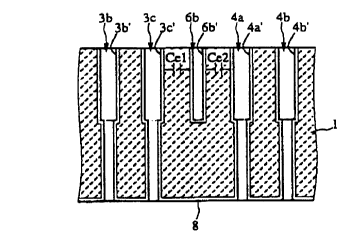
Fig. 2 is a sectional view in part of the antenna
sharing unit shown in Fig. 1: Fig. 2A is a sectional view
along the axis of the internal-conductor through-holes; and
Fig. 2B is a sectional view in the direction perpendicular
to the axis of the internal-conductor through-holes. In
Fig. 2, reference numerals 3b', 3c', 4a' and 4b' indicate
internal conductors formed within the through-holes 3b, 3c,
and 4a and 4b, respectively, and 6b' represents an electrode
disposed within the slit 6b. In this embodiment the slit 6b
CA 0221~803 1997-09-18
is formed on the exposed surface, i.e., on the surface
having high electric-field energy, between the adjacent
internal conductors 3c' and 4a' so as to receive the
electrode 6b' therein. This inhibits unwanted coupling of
the resonators formed by the internal conductors 3c' and
4a'. Meanwhile, external coupling capacitors Cel and Ce2
are formed between the electrode 6b' and the internal
conductor 3c' and between the electrode 6b' and the internal
conductor 4a', respectively, thereby forming an external-
coupling circuit shared by the two filters. In the
embodiment shown in Figs. 1 and 2, the internal-conductor
through-holes having the same internal diameters are
disposed at an equal pitch (a constant pitch). However, the
through-holes may have different internal diameters and also
may be disposed at different pitches between the
transmitting filter and the receiving filter in response to
the required characteristics of the respective filters
(which will be described in detail later). Further, in this
embodiment the through-holes are configured as stepped
through-holes (the internal diameters vary stepwise) in
accordance with the respective required filter
characteristics. The position of the steps may be different
between the through-holes, and the depth of the slit is not
necessarily on the same level as the position of the steps.
Fig. 3 is an equivalent circuit of the antenna sharing
CA 0221~803 1997-09-18
--10--
unit shown in Fig. 1. In Fig. 3, R2 designates a resonator
formed by the through-hole 2 shown in Fig. 1 (strictly
speaking, although the resonator is formed by the internal
conductor provided in the through-hole 2, the dielectric
block 1 and the external conductor 8, it is simply referred
to as "the resonator formed by the through-hole 2); R3a, R3b
and R3c indicate resonators formed by the through-holes 3a,
3b and 3c, respectively; R4a, R4b, R4c and R4d represent
resonators formed by the through-holes 4a, 4b, 4c and 4d,
respectively; and R5 depicts a resonator formed by the
through-hole 5. The resonators R3a through R3c serve as a
band-pass filter (BPF) formed of three stages of resonators,
while the resonators R4a through R4d function as a BPF
formed of four stages of resonators. The resonators R2 and
R5 each serve as a trap circuit formed of a one-stage
resonator. Further, Ca and Cb indicate capacitors generated
between the conductor within the through-hole 2 and the
electrode within the slit 6a and between the conductor
within the through-hole 3a and the electrode within the slit
6a, respectively, whiie Cc and Cd designate capacitors
produced between the conductor within the through-hole 5 and
the electrode within the slit 6c and between the conductor
within the through-hole 4d and the slit 6c, respectively.
Moreover, Cel and Ce2 represent capacitors generated between
the conductor within the through-hole 3c and the electrode
CA 0221~803 1997-09-18
within the slit 6b and between the conductor within the
through-hole 4a and the electrode within the slit 6b,
respectively. With this configuration, the following type
of antenna sharing unit can be constructed in which the
resonators R2, R3a, R3b and R3c serve as a transmitting
filter, while the resonators R5, R4a, R4b, R4c and R4d
function as a receiving filter. Namely, the unit shown in
Fig. 1 is used as an antenna sharing unit in which the
input/output electrodes 7a, 7b and 7c serve as a
transmitting-signal (Tx) input electrode, an antenna-
connecting (ANT) electrode, and a receiving-signal (Rx)
output electrode, respectively.
An explanation will now be given of the configuration
of an antenna sharing unit according to a second embodiment
of the present invention with reference to Figs. 4 and 5.
Fig. 4 illustrates the antenna sharing unit which is
vertically placed. For practical use, the unit is surface-
mounted on a board with the top surface of the block 1 or
the surface on the proximal side of Fig. 4 in contact with
the board. In the second embodiment, unlike the first
embodiment, substantially all the surfaces of the block 1
are covered with the external conductor 8 rather than being
exposed. Further, the input/output electrodes 7a, 7b and 7c
are extended to the exposed surface of the block 1 on which
the through-holes 2, 3a through 3c, 4a through 4d, and 5 are
CA 0221~803 1997-09-18
formed. Fig. 5 is a sectional view in part along the axis
of the internal-conductor through-holes.
Fig. 5 reveals that a conductor-free region is provided
in part of each through-hole so as to divide the conductors
into the resonator electrodes 3b', 3c', 4a' and 4b' and the
forward-end capacitor electrodes 3b~, 3c~, 4a~ and 4b~,
respectively. Likewise, the other internal conductors are
divided into the corresponding resonator electrodes and the
forward-end capacitor electrodes. Further, in this
embodiment the through-holes 3a through 3c are configured as
straight holes (having a constant internal diameter), while
the through-holes 4a through 4d are configured as stepped
holes (the internal diameter varies stepwise). It is thus
possible to respond to the required characteristics of the
respective filters. With this arrangement, the internal-
conductor through-holes 3a through 3c are comb-line-coupled
to each other to form three stages of resonators serving as
a BPF, while the internal-conductor through-holes 4a through
4d are comb-line-coupled to each other to form four stages
of resonators serving as a BPF. The through-holes 2 and 5
are each used as a trap circuit. Further, capacitors are
generated between the electrode within the slit 6a and the
resonator electrode within the through-hole 2 and between
the electrode within the slit 6a and the resonator electrode
within the through-hole 3a, respectively; capacitors are
CA 0221~803 1997-09-18
produced between the electrode within the slit 6b and the
resonator electrode within the through-hole 3c and between
the electrode within the slit 6b and the resonator electrode
within the through-hole 4a; and capacitors are generated
between the electrode within the slit 6c and the resonator
electrode within the through-hole 4d and between the
electrode within the slit 6c and the resonator electrode
within the through-hole 5. Accordingly, in this embodiment,
as well as the previous embodiment, the input electrodes 7a,
7b and 7c, continuously ext~n~;ng from the electrodes formed
within the slits 6a, 6b and 6c, can be used as a Tx
electrode, an ANT electrode, and a Rx electrode,
respectively. Additionally, in the second embodiment shown
in Fig. 4, since the input/output electrodes 7a, 7b and 7c
extend to the top surface of the block 1, the top surface
may be used as a mounting surface.
The configuration of an antenna sharing unit according
to a third embodiment of the present invention will now be
described while referring to Fig. 6. The antenna sharing
unit of the third embodiment is a modification made to the
unit shown in Fig. 1, and is partially shown in Fig. 6.
Fig. 6 reveals that the slit 6a is formed to pass through
the dielectric block 1 in the widthwise direction, and an
electrode-free portion 9 is disposed in the slit 6a to
establish an insulation between the electrode within the
CA 022l~803 l997-09-l8
-14-
slit 6a and the external conductor 8.
Fig. 7A is a perspective view in part of an antenna
sharing unit according to a fourth embodiment of the present
invention. Fig. 7B is a rear view of the unit shown in Fig.
7A and shows that on the surface of the slit 6a an
electrode-free portion 9 is formed as a tapered notch on
which the input/output electrode 7a is not formed. Thanks
to the electrode-free portion 9, the electrode within the
slit 6a and the external conductor 8 can be insulated.
Fig. 8 is a perspective view in part of an antenna
sharing unit according to a fifth embodiment of the present
invention. Although linear slits are provided for the first
through the fourth embodiments, in the fifth embodiment the
slits are branched off in a midpoint into a plurality of
portions. Fig. 8A illustrates an antenna sharing unit in
which a T-shaped slit in cross section is formed; Fig. 8B
illustrates a unit in which a predetermined portion of the
T-shaped slit is curved; and Fig. 8C illustrates a unit in
which a hook-shaped slit in cross section is formed. This
configuration makes it possible to increase the opposing
areas between the electrode within the slit and each of the
internal conductors within the two adjacent through-holes
across the slit. As a consequence, the required capacitance
can be easily obt~ine~ even though, for example, the depth
of the slit is decreased.
CA 022l~803 l997-09-l8
-15-
Fig. 9 illustrates an antenna sharing unit according to
a sixth embodiment of the present invention. In the fifth
embodiment illustrated in Fig. 8, the slit 6a is extended to
the portion between the through-hole and the lateral surface
of the dielectric block 1 so as to obtain a sufficient
capacitance between the electrode within the slit and the
conductor within the through hole. In the sixth embodiment,
however, the width of the slit 6a along which the through-
holes are arranged is enlarged, as shown in Figs. 9A and 9B,
to decrease the distance between the internal conductor in
the through-hole and the electrode within the slit 6a,
thereby ensuring the required capacitance therebetween. In
particular, in the embodiment shown in Fig. 9B, not only the
width of the slit 6a along which the through-holes are
arranged is enlarged, but also the slit 6a is extended to
the portion between the through-holes and the lateral
surface of the dielectric block 1, thereby obt~;n;ng the
required capacitance between the slit 6a and each of the
adjacent through-holes.
Fig. 10 is a perspective view in part of an antenna
sharing unit according to a seventh embodiment of the
present invention. In the first through the sixth
embodiments, the input/output electrodes, extending from the
electrodes within the respective slits, are provided. In
the seventh embodiment, however, capacitance is generated
CA 0221~803 1997-09-18
-16-
between the electrode within the slit and the input/output
electrode, thereby performing input and output of signals.
Namely, only the top surface of the dielectric block 1 is
opened, as shown in Fig. 10, by providing the slit 6a.
Then, the input/output electrode 7a is provided on the
lateral surface of the dielectric block 1 which opposedly
faces the electrode within the slit 6a so as to produce
capacitance between the input/output electrode 7a and the
electrode within the slit 6a. In order to increase the
capacitance between the electrode within the slit 6a and the
input/output electrode 7a, the opposing areas therebetween
may be increased or the distance therebetween may be
decreased, as illustrated in Figs. lOA and lOB. Further, in
order to elevate the capacitance between the electrode
within the slit 6a and each of the conductors within the
adjacent through-holes, as well as to increase the
capacitance between the electrode within the slit 6a and the
input/output electrode 7a, the slit 6a may be configured, as
shown in Fig. lOB, to increase the opposing areas between
the electrode within~the slit 6a and the internal conductors
within the adjacent through-holes.
Although in the foregoing embodiments a single antenna
sharing unit is formed within a single dielectric block, a
plurality of antenna sharing unit may be disposed. In this
case, a plurality of input/output electrodes may be provided
CA 0221~803 1997-09-18
-17-
within a single dielectric block; and among the electrodes a
plurality of input/output electrodes may be used as
transmitting/receiving-signal connecting electrodes, while
others may be employed as a plurality of transmitting-signal
input electrodes and a plurality of receiving-signal output
electrodes. Moreover, although each of the above-described
embodiments is used as an antenna sharing unit, the present
invention may serve as a general transmitting/receiving-
sharing unit (duplexer) in which an antenna connecting
electrode is connected not to an antenna but to, for
example, a transmission line through which transmitting and
receiving signals are transmitted.
Similarly, a multiplexer may be formed within a
dielectric block in the following m~nn~r. A plurality of
internal conductors, slits each having an electrode therein,
and input/output electrodes may be provided within a
dielectric block. Among the above electrodes, a
predetermined input/output electrode may be used as an
output-signal or input-signal connecting electrode. If the
above electrode is used as an output-signal connecting
electrode, the other electrodes may serve as input-signal
connecting electrodes, and vice versa. More specifically,
in a manner substantially similar to the configuration
illustrated in Figs. 1 through 4, transmitting filters may
be formed across the input/output electrode 7b, and the
CA 022l~803 l997-09-l8
-18-
input/output electrode 7b may be used as an output-signal
connecting electrode, while the input/output electrodes 7a
and 7c may be employed as input-signal connecting
electrodes. Thus, a two-input and one-output multiplexer
(diplexer) may be constructed. Further, a plurality of rows
of internal-conductor through-holes may be formed in a
dielectric block, and three or more sets of dielectric
filters may be each disposed across one input/output
electrode. The input/output electrode may be used as an
output-signal connecting electrode, while the other
input/output electrodes may be employed as input-signal
connecting electrodes. As a result, a multi-input and one-
output multiplexer may be formed. Alternatively, the
input/output relationships may be reversed to form a one-
input and multi-output multiplexer.
As is seen from the foregoing description, the present
invention offers the following advantages.
A slit having an electrode therein is provided between
two adjacent internal conductors so as to disconnect them,
thereby preventing unwanted coupling between the two filters
across the above-described slit. Thus, the distance between
the two filters can be decreased to ~nhAnce the
miniaturization of the overall dielectric filter unit.
Further, a plurality of internal conductors may be
disposed within a dielectric block, and a slit having an
CA 0221~803 1997-09-18
--19--
electrode therein and an input/output electrode are provided
at least in three areas of the block. Only with this
arrangement, easy designing of a compact
transmitting/receiving-sharing unit can be enhanced.
Additionally, a plurality of internal conductors may be
arranged within a dielectric block, and a slit having an
electrode therein and an input/output electrode are provided
at least in three areas of the block. Only with this
configuration, simple designing of a downsized multiplexer
can be facilitated.