Note: Descriptions are shown in the official language in which they were submitted.
CA 02216357 1997-09-23
-1-
DC/AC POWER CONVERTER
BACKGROUND OF THE INVENTION
This invention relates to DC/AC power converters, and more
particularly to bi-directional DC/AC power converters.
Prior art bi-directional DC/AC power converters can be
divided into three categories including: line frequency
transformer, non-sinusoidal converters; line frequency
transformer, sinusoidal converters; and high frequency
transformer, sinusoidal converters.
Line frequency transformer non-sinusoidal converters
typically employ an H-bridge of switching elements
connected to a primary winding of a transformer designed to
operate at AC line frequencies and phase control switching
elements connected to a secondary winding of the
transformer. Switching of the switching elements forming
the H-bridge is controlled to produce a quasi-squarewave at
the primary winding of the transformer, and this quasi
square wave is stepped up by the turns ratio of the
transformer. The secondary winding of the transformer
produces an output waveform which is commonly called a
quasi sinewave or a modified sinewave. Regulation of the
root mean square value of the output voltage of the
converter is achieved by varying the duty cycle of the
waveform. The phase controlled switch is employed to
regulate charging current, in the charging mode. By
advancing or retarding the phase angle relative to the zero
crossing of the AC voltage, the current can be increased or
decreased. Power converters of this type have
disadvantages in that the output voltage in inverter mode
is non-sinusoidal and is only regulated for its Root Mean
Square (RMS) value. Some loads are sensitive to non-
sinusoidal waveforms and only operate well when the applied
voltage is sinusoidal. Others are sensitive to the peak
voltage of the AC waveform and require regulation of the
CA 02216357 1997-09-23
-2-
peak voltage close to the peak voltage of the sinewave
voltage. In addition, with this type of power converter a
pulsating current is drawn from the battery, in the
inverter mode, as there is no or little internal energy
storage within the converter. In addition, power factor in
the charger mode is low and current distortion is high. In
addition, charging current is pulsating and, finally, the
line current transformer is relatively large and heavy,
limiting the applications of the converter.
With power converters of the line frequency transformer,
sinusoidal type, it is common to find a multi-transformer
configuration having secondary windings wired in series and
primary windings connected to an H-bridge of switches. By
controlling the switching sequence of the switches, a
stepped sinusoidal voltage is produced on the secondary
windings. Switching H-bridges may also be controlled to
convert an AC voltage applied to the transformer secondary
winding to produce a DC voltage for battery charging.
United States Patent number 5,373,433 to Thomas discloses
this approach.
Line frequency transformer, sinusoidal inverter/chargers
also include a line frequency transformer with a
multi-tapped secondary winding. The transformer also has
a primary winding which is driven with a quasi-squarewave
as described above. Bi-directional switches selectively
connect the taps of the secondary winding to the output to
produce a roughly stepped approximation of a sinusoidal
output voltage. This approach is disclosed in United
States Patent number 5,155,672 to Brown.
Uninterruptible power supply circuits also normally fall
into the line frequency transformer sinusoidal inverter
charger category as they involve an H-bridge controlled by
sinusoidal pulse width modulation to produce a sinusoidal
line frequency voltage at primary terminals of a line
CA 02216357 2001-06-15
-3-
frequency transformer. The line frequency transformer
provides a step up or step down in voltage and galvanic
isolation between the DC port and AC port. This circuit,
however, lacks internal energy storage and therefore,
produces pulsating currents at the DC port in both the
inverter and charger modes. In addition, such devices are
large and heavy because they require one or more low
frequency transformers.
Power converters of the high frequency transformer,
sinusoidal type include bi-directional DC to high
frequency AC converter stages which are connected to a low
voltage winding of a high frequency transformer. A power
converter of this type is described in United States
Patent No. 4,742,441 to Akerson. The high frequency
transformer provides voltage step up and step down and
galvanic isolation. A high voltage winding of the
transformer is typically connected to a high frequency AC
to low frequency AC cycloinverter, -the output of which is
used to source power to an AC load or receive power
therefrom. Use of the cycloinverte~r requires the use of
bi-directional switches which, with present technology,
must be constructed as composite assemblies of
uni-directional switches. In addition, the switches in
the DC to high frequency conversion stage and the high
frequency AC to low frequency AC conversion stage must be
precisely synchronized when switching to avoid destroying
the switching elements. This requires complex control
circuits.
BRIEF SUMMARY OF THE INVENTION
In accordance with one aspect of the invention, there is
provided a DC link power converter apparatus including a
first DC to DC converter, a DC to AC converter and a load
balancing storage element. The fir~~t DC to DC converter
has first and second DC ports and the DC to AC converter
CA 02216357 2001-06-15
-4-
has a third DC port and has an AC port and is controllable
as a current fed transformer isolated boost step up
converter to transfer energy from tree first DC port to the
second DC port. The first DC port is connectable to a DC
source and the second DC port is connected to the third DC
port. The AC port is connectable to an AC load. The load
balancing energy storage element is connected to the
second DC port for decoupling the DC to DC converter from
the DC to AC converter by supplying energy to the third DC
port when a voltage at the second DC port is tending to
decrease and for storing energy received from the second
DC port when a voltage at the third port is tending to
increase.
The DC to AC converter may be bidirectional. The first DC
to DC converter may be controllable as a voltage fed
transformer isolated buck step down converter for
transferring energy from the second DC port to the first
DC port.
The apparatus may include a DC bus connecting the second
and third DC ports together for transferring energy
between the DC to DC converter and the DC to AC converter,
the load balancing energy storage f~lement decoupling the
DC to DC converter from the DC to AC converter by
supplying energy to the DC bus when a voltage at the DC
bus is tending to decrease and for motoring energy received
from the DC bus when a voltage at th.e DC bus is tending to
increase. The load balancing energy storage element may
include a capacitor.
The DC to DC converter may include a first power control
circuit and the DC to AC converter may include a second
power control circuit, the first and second power control
circuits operating independently of Esach other.
The DC to DC converter may include a centre-tapped
CA 02216357 2001-06-15
-5-
transformer, an input inductor, .and first and second
switching elements. The centre-tapped transformer may
include a centre-tapped primary winding having a number of
turns, first and second primary winding terminals and a
centre-tap terminal and a secondary winding having first
and second secondary winding terminals. The input
inductor may be connected between the centre-tap terminal
and the first terminal of the first DC port and the first
and second switching elements may be connected between the
first and second primary winding terminals respectively
and a second terminal of the first DC port.
The first and second switching elements may be
unidirectional and may include transistors.
The DC to DC converter may include a first inverter mode
control circuit for controlling power flow from the first
DC port to the DC bus, and a first charge mode control
circuit for controlling power flow :From the DC bus to the
first DC port.
The DC to DC converter may include a first inverter mode
control circuit for controlling power flow in the DC to DC
converter.
The first inverter mode control circuit may be operable to
control the DC to DC converter as a push-pull, current-fed
transformer-isolated boost converter.
The first inverter mode control circuit may include a
current control loop circuit for generating a current
feedback signal responsive to current at the first DC
port, a voltage control loop circuit for generating a
current command signal in response to DC bus voltage and a
first switching control circuit for producing switching
control signals in response to the current feedback signal
and the current command signal for controlling switching
CA 02216357 2001-06-15
-6-
of the first and second switching elements.
The voltage control loop circuit may include a DC bus
voltage feedback signal generator for generating a DC bus
voltage feedback signal indicative of the DC bus voltage
and a non-linear voltage loop compensation network
responsive to the DC bus feedback signal for producing the
current command signal, the non-linear voltage loop
compensation network having a relatively slow response in
changing the current command signal when the DC bus
voltage feedback signal is changing relatively slowly and
the non-linear voltage loop compensation network having a
relatively fast response in changing the current command
signal when the DC bus voltage feedback signal is changing
relatively quickly.
The voltage control loop circuit may include a DC bus
voltage reference source for producing a DC bus voltage
reference signal and a first subtracter for subtracting
the DC bus voltage reference signal from the DC bus
voltage feedback signal to produce a first voltage error
signal, the voltage error signal being communicated to the
non-linear voltage loop compensation network, and the non-
linear voltage loop compensation network may produce the
current command signal in response to the voltage error
signal.
The non-linear voltage loop compensation circuit may
include a first low pass filter and at least one diode in
parallel with the first low pass filter, the diode being
operable to forward conduct when the voltage error signal
changes at a rate at which an instantaneous voltage drop
across the low pass filter exceeds a pre-defined value.
The first switching control circuit may include a second
subtracter for subtracting the current feedback signal
from the current command signal to produce a first current
CA 02216357 2001-06-15
error signal, a second low pass filter for filtering the
first current error signal to produce a duty cycle command
signal and a first pulse width modulator for producing
first and second switching signals for placing the first
and second switching elements respectively in conducting
and non-conducting modes for periods of time dependent on
the duty cycle command signal.
The first pulse width modulator may include first and
second waveform generators for generating first and second
waveforms 180 degrees out of phase with each other, the
first and second waveforms may include at least an on
state and an off state and having a first duty cycle, the
first and second waveforms being supplied to the first and
second switching elements respectively to place the
switching elements in conducting and non-conducting modes
according to the on and off states respectively, of the
first and second waveforms respectively.
The first inverter mode control circuit may include a
first circuit portion connected to the primary winding and
a second circuit portion connected to the DC bus, and a
first isolator for isolating the first circuit portion
from the second circuit portion while providing for
communication between the first and second circuit
portions. The first isolator may include an optical
isolator.
The apparatus may include at least a first clamping
circuit for controlling the voltage across at least one of
the first and second switching elements.
The clamping circuit may include a second DC to DC
converter connected between at least: one of the first and
second switching elements and the first terminal of the DC
port.
CA 02216357 2001-06-15
_8_
The DC to DC converter may include a first charge mode
control circuit for controlling power flow from the DC bus
to the first DC port. The first and second switching
elements may include first and sec;ond low voltage metal
oxide semiconductor field effect (MOSFET) transistors
having first and second antiparallel diodes respecively.
The first charge mode control circuit may be operable to
control the DC to DC converter as a full-bridge voltage
fed transformer-isolated buck step-down converter.
The apparatus may include third, fourth, fifth and sixth
switching elements connected to the secondary winding in a
full bridge topology.
The first DC to DC converter may include a second
switching control circuit in communication with the third,
fourth, fifth and sixth switching elements for controlling
conduction of the third, fourth, fifth and sixth switching
elements to produce a high frequency voltage waveform
across the secondary winding.
The second switching control circuit may include a
switching signal generator for generating third, fourth,
fifth and sixth control signals responsive to voltage at
the first DC port and current at the second DC port; the
third, fourth, fifth and sixth control signals being
operable to place the third, fourth, fifth and sixth
switching elements in conducting and non-conducting
states.
The control signal generator may include a bridge current
command signal generator for producing a bridge current
command signal in response to voltage and current at the
first DC port, a bridge current feedback signal generator
for producing a bridge current feedback signal in response
to current drawn at the second DC port, a third subtracter
CA 02216357 2001-06-15
-9-
for subtracting the bridge current feedback signal from
the bridge current command signal to produce a duty cycle
command signal and a second pulse width modulator
responsive to the duty cycle command signal for producing
the third, fourth, fifth and siacth switching signals
operable to control switching of the third, fourth, fifth
and sixth switching elements.
The bridge current feedback signal generator may include
first and second current sense :signal generators for
generating first and second current sense signals
representing current flow in the fourth and sixth
switching elements respectively, a summer for summing the
first and second current sense signals to produce a raw
bridge current feedback signal and a. third low pass filter
for filtering the raw bridge current feedback signal to
produce the bridge current feedback signal.
The bridge current command signal generator may include a
current error signal generator for generating a second
current error signal in response tb current flow at the
first DC port, a voltage error signal generator for
generating a second voltage error signal in response to
voltage at the first DC port, a ~~ignal selector having
first and second inputs for receiving the second current
error signal and the second voltage error signal and an
output for producing a lesser output signal responsive to
the lesser of the second current error signal and the
second voltage error signal, a second isolator having an
input electrically connected to the first DC port, for
receiving the lesser output signal and an output
electrically connected to the DC bus for providing the
bridge current command signal to the third subtracter, the
input and output being electrically isolated from each
other.
The current error signal generator rriay include, a charging
CA 02216357 2001-06-15
-10-
current signal generator for generat:ing a charging current
signal generator for generating a charging current signal
indicative of current at the first DC port, a fourth low
pass filter for filtering the charging current signal to
produce a filtered charging current signal, a charge
current command signal generator for generating charging
current command signal indicative of a desired charging
current, and a fourth subtracter for subtracting the
filtered charging current signal from the charge current
command signal to produce the second current error signal.
The voltage error signal generator may include a charging
voltage signal generator for generating a charging voltage
signal indicative of voltage at the first DC port, a
charging voltage reference signal generator for generating
a charging voltage reference signal indicative of a
desired charging voltage, a fifth subtracter for
subtracting the charging voltage signal from the charging
voltage reference signal to producs~ a raw voltage error
signal, and a second non-linear voltage loop compensation
network for filtering the raw voltage error signal to
produce the second voltage error signal.
The second non-linear voltage loop compensation network
may include a fifth low pass filter.
The second non-linear voltage look> compensation network
may have a relatively slow loop response when the raw
voltage error signal is changing relatively slowly and a
relatively fast loop response when the raw voltage error
signal is changing relatively quickly.
The second non-linear voltage loop compensation network
may be operable to provide a slow response when the raw
voltage error signal is changing relatively slowly and a
fast response when the raw voltage error signal is
changing relatively quickly.
CA 02216357 2001-06-15
-11-
The DC to AC converter may include a full bridge converter
having an input connected to the DC bus and a bridge
output for providing a pulse width modulated waveform, and
an AC output low pass filter having an input connected to
the bridge output for receiving the pulse width modulated
waveform and a filter output, the filter output acting as
the AC port.
The full bridge converter may include seventh, eighth,
ninth and tenth switching elements connected to the DC bus
in a full bridge topology.
The DC to AC converter may include an AC current sense
signal generator for generating an P,C current sense signal
responsive to current at the bridge output, a DC bus
voltage sense signal generator for' generating a DC bus
voltage sense signal responsive to voltage at the DC bus,
an AC output voltage sense signal generator for generating
an output voltage sense signal responsive to voltage at
the bridge output, an inverter mode current command signal
generator for generating an inverter mode current command
signal in response to the AC voltage sense signal, and a
third switching control circuit for producing switching
signals for controlling the seventh, eighth, ninth and
tenth switching elements in response to the inverter mode
current command signal.
The DC to AC converter may include a DC bus voltage sense
signal generator for generating a DC bus voltage sense
signal responsive to voltage at the DC bus, a DC bus
voltage reference signal generator for generating a DC bus
voltage reference signal, a current waveform signal
generator for generating a desired current waveform signal
indicative of the desired current at the bridge output, a
charge mode current command signal generator for
generating a charge mode command signal in response to the
CA 02216357 2001-06-15
-12-
DC bus voltage sense signal, the DC'. bus voltage reference
signal and the desired current waveform signal, and a
third switching control circuit for producing switching
signals for controlling the seventh, eighth, ninth and
tenth switching elements in response to the charge mode
command signal.
The DC to AC converter may include a DC bus voltage sense
signal generator for generating a DC bus voltage sense
signal responsive to voltage at the DC bus, a DC bus
voltage reference signal generator f:or generating a DC bus
voltage reference signal, a current waveform signal
generator for generating a desired current waveform signal
indicative of the desired current at. the bridge output, an
AC current sense signal generator for generating an AC
current sense signal responsive to current at the bridge
output, an AC output voltage sense: signal generator for
generating an AC output voltage sense signal responsive to
voltage at the bridge output, a charge mode current
command signal generator for generating a charge mode
command signal in response to the DC bus voltage sense
signal, the DC bus voltage reference signal and the
current waveform signal, an inverter mode current command
signal generator for generating an inverter mode current
command signal in response to the voltage sense signal, a
third switching control circuit fc>r producing switching
signals for controlling the switching elements in response
to the AC current sense signal, the DC bus voltage
reference signal and at least one of the charge mode
command signal and the inverter mode command signal, and a
selector in communication with the' charge mode command
signal generator, the inverter mode current command signal
generator, and the switching signal generator for
selectively providing the inverter mode current command
signal or the charge mode current command signal to the
switching control circuit.
CA 02216357 2001-06-15
-13-
The inverter mode current command signal generator may
include a DC offset correction circuit for varying the
inverter mode current command signal in response to DC
offset voltage at the bridge output.
The DC offset correction circuit may include a sixth low
pass filter for producing a filtered DC offset signal in
response to the AC output voltage sense signal, a sinewave
reference signal generator for generating a sinewave
reference signal, a sixth subtracter for subtracting the
filtered DC offset signal from the sinewave reference
signal to produce an output voltage command signal, and a
seventh subtracter for subtracting the AC output voltage
sense signal from the output voltage command signal to
produce the current command signal.
The charge mode current command signal generator may
include an eighth subtracter for subtracting the DC bus
voltage sense signal from the DC bus voltage reference
signal to produce an average current signal, and a
multiplier for multiplying the average current signal by
the current desired waveform signal to produce the charge
mode current command signal.
The third switching control circuii~ may include a third
duty cycle command signal generator for generating a third
duty cycle command signal indicative of a desired duty
cycle of the seventh, eighth, ninth and tenth switching
elements, a third pulse width modulator for producing a
width-modulated pulse stream in response to the third duty
cycle command signal, and a gate drive decoder circuit for
generating switching element control signals for
controlling the seventh, eighth, ninth and tenth switching
elements in response to the width-modulated pulse stream.
The gate drive decoder circuit may include a programmable
array logic device.
CA 02216357 2001-06-15
-14-
The third switching control circuit may include a
magnetization compensation circuit for compensating the
third duty cycle command signal in response to the
magnitude of current at the bridge output to compensate
for magnetization effects in the AC output low pass
filter.
The magnetization compensation circuit may include a
variable gain amplifier in communication with the third
pulse width modulator for amplifying the third duty cycle
command signal to provide an amplified third duty cycle
command signal to the third pulse width modulator, the
variable gain amplifier having a gain dependent upon the
AC current sense signal.
The switching control circuit may be operable to switch
the seventh and tenth switching elements in unison,
between a conducting state and a non-conducting state and
may be operable to switch the eighi~h and ninth switching
elements in unison, between a condu~~ting state and a non-
conducting state such that a dead time is provided when
switching the seventh and tenth switching elements from a
conducting state to a non-conducting state and when
switching the eighth and ninth switching elements between
the conducting state and the non-conducting state, the
deadtime being a period during which each of the seventh,
eighth, ninth and tenth switching elements is in a non-
conducting state.
The DC to AC converter may include a snubber circuit
connected between the bridge output and the DC bus.
The snubber circuit may include eleventh and twelfth
switching elements connected to the bridge output, second
and third inductors connected to the eleventh and twelfth
switching elements respectively and connected to each
CA 02216357 2001-06-15
-15-
other, and a diode connected to the second and third
inductors and the DC bus.
The third switching control circuit may be operable to
control the eleventh and twelfth switching elements in
response to the DC bus voltage sense signal and the AC
current signal.
The third switching control circuit: may produce eleventh
and twelfth switching signals for controlling the eleventh
and twelfth switching elements t:o place the snubber
circuit in communication with the bridge output for a
period of time dependent upon current at the AC port and
DC bus voltage.
The third switching control circuit may be operable to
vary the period of time in response to the DC bus voltage
sense signal and the AC current sense signal.
In accordance with another aspect of the invention, there
is provided a method of transferring power between a DC
port and an AC port. The method involves:
a) selectively operating a DC'. to DC converter in at
least one of a current fed transformer isolated
boost mode and a voll~age fed transformer
isolated buck mode to transfer energy between
the DC port and a DC bus;
b) selectively operating a DC to AC converter in at
least one of an invert mode and a charge mode to
transfer energy between the DC bus and the AC
port; and
c) supplying energy to the DC bus from a load
balancing energy storage Element when a voltage
at the DC bus is tending to decrease and storing
CA 02216357 2001-06-15
-16-
energy from the DC bus in the energy storage
element when a voltage at the DC bus is tending
to increase.
In accordance with another aspect of the invention, there
is provided a power converter apparatus including first
and second simultaneously operable :DC to DC converters, a
DC bus, a first DC to AC converter, a second DC to AC
converter, and a load balancing enesrgy storage element.
The first and second DC to DC converters are connectable
to a common DC source and each have first and second DC
ports connected together. The DC bus is connected to the
second DC ports. The first DC to AC" converter has a third
DC port connected to the DC bus and a first AC port
connectable to an AC source, the first DC to AC converter
being bi-directional and operable in an AC to DC
conversion mode. The second DC t.o AC converter has a
fourth DC port and a second AC port, the fourth DC port
being connected to the DC bus and the second AC port being
connected to an AC load. The load balancing energy
storage element is connected to the DC bus for decoupling
the first and second DC to DC converters and the second DC
to AC converter from the first DC to AC converter by
supplying energy to the DC bus when a voltage at the DC
bus is tending to decrease and for storing energy received
from the DC bus when a voltage at the DC bus is tending to
increase.
The first and second DC to AC converters may be bi-
directional.
The first and second DC to DC converters may be bi-
directional.
The first and second DC to DC converters may include first
and second current control loop circuits respectively for
controlling the flow of power through the first and second
CA 02216357 2001-06-15
-17-
DC to DC converters respectively.
The apparatus may include a DC to DC converter control
circuit for providing current command signals to the first
and second current control loop circuits respectively for
apportioning contributions of energy to the load balancing
energy storage element between the first and second DC to
DC converters.
The first DC to AC converter may include a third current
control loop circuit for controlling the flow of power
through the first DC to AC converter.
The apparatus may include a DC to AC converter control
circuit for providing a current command signal to the
third current control loop circuits for controlling the
flow of power through the first DC to AC converter.
The apparatus may include a fourth current control loop
circuit for controlling the flow of power through the
second DC to AC converter.
The apparatus may include a DC to AC converter control
circuit for providing a current command signal to the
fourth current control loop circuit for controlling the
flow of power through the second DC 'to AC converter.
The first and second DC to DC converters may be bi
directional and the first DC to AC converter and first DC
to AC converter may be bi-directional.
In accordance with another aspect o.f the invention, there
is provided a power converter apparatus .including first
and second simultaneously operable DC to DC converters, a
DC bus, first and second DC to AC converters, and a load
balancing energy storage element. The first and second DC
to DC converters are connectable to a common DC source,
CA 02216357 2001-06-15
-18-
and each has first and second DC ports, the second DC
ports being connected together. The DC bus is connected
to the second DC ports. The first and second DC to AC
converters have third DC ports connected to the DC bus
respectively and respective first AC ports for supplying
power to first and second AC loads .respectively. The load
balancing energy storage element is connected to the DC
bus for decoupling the first and second DC to DC
converters from the first and second DC to AC converters
by supplying energy to the DC bus when a voltage at the DC
bus is tending to decrease and for storing energy received
from the DC bus when a voltage at the DC bus is tending to
increase.
The first and second DC to DC converters may include first
and second current control loop circuits respectively for
controlling the flow of power through the first and second
DC to DC converters respectively.
The apparatus may include a DC to DC converter control
circuit for providing current command signals to the first
and second current control loop circuits respectively for
apportioning contributions of energy to the load balancing
energy storage element between the first and second DC to
DC converters.
The first DC to AC converter may include a third current
control loop circuit for controlling the flow of power
through the first DC to AC converter.
The apparatus may include a firsi~ DC to AC converter
control circuit for providing a current command signal to
the third current control loop circuit for controlling the
flow of power through the first DC to AC converter.
The second DC to AC converter includes a fourth current
control loop circuit for controlling the flow of power
CA 02216357 2001-06-15
-19-
through the second DC to AC converter.
The apparatus rnay include a second DC to AC converter
control circuit for providing a current command signal to
the fourth current control loop circuit for controlling
the flow of power through the second. DC to AC converter.
The first and second DC to AC converter control circuits
may control the first and second DC to AC converters such
that the first and second DC to AC converters produce
first and second AC waveforms respectively, the first and
second AC waveforms being out of phase with each other.
The apparatus may include a reference signal generator for
generating first and second AC waveform reference signals,
the first and second AC waveform reference signals being
provided to the first and second DC to AC converter
control circuits respectively.
The first and second DC to DC converters may be bi-
directional and the first and second DC to AC converters
may be bi-directional.
The first and second DC to AC converters may include third
and fourth current control loop circuits respectively for
controlling the flow of power through the first and second
DC to AC converters.
The apparatus may include a first, DC to AC converter
control circuit for providing third and fourth current
command signals to the third and :Fourth current control
loop circuits respectively for controlling the flow of
power through the first and second DC to AC converters.
In accordance with another aspect of the invention, there
is provided a power converter apparatus including first
and second simultaneously operable DC to DC converters, a
CA 02216357 2001-06-15
-20-
DC bus, first and second DC to AC converters, and a load
balancing energy storage element. The first and second DC
to DC converters are connectable t.o first and second DC
sources respectively. The first and second DC to DC
converters each have first and second DC ports, the second
DC ports being connected togethE:r. The DC bus is
connected to the second DC ports. '.Che first and second DC
to AC converters have third DC port s connected to the DC
bus respectively and respective first AC ports for
supplying power to first and second AC loads respectively.
The load balancing energy storage element is connected to
the DC bus for decoupling the first and second DC to DC
converters from the first and second DC to AC converters
by supplying energy to the DC bus when a voltage at the DC
bus is tending to decrease and for :storing energy received
from the DC bus when a voltage at the DC bus is tending to
increase.
The first and second DC to DC converters may include first
and second current control loop circuits respectively for
controlling the flow of power through the first and second
DC to DC converters respectively.
The apparatus may include first and second DC to DC
converter control circuits' for providing first and second
current command signals to the first and second current
control loop circuits respectively for independently
controlling power flow through the first and second DC to
DC converters.
The first DC to AC converter may include a third current
control loop circuit for controlling the flow of power
through the first DC to AC converter.
The apparatus may include a firsi~ DC to AC converter
control circuit for providing a current command signal to
the third current control loop circuit for controlling the
CA 02216357 2001-06-15
-21-
flow of power through the first DC to AC converter.
The second DC to AC converter may include a fourth current
control loop circuit for controlling the flow of power
through the second DC to AC converter.
The apparatus may include a second DC to AC converter
control circuit for providing a current command signal to
the fourth current control loop circuit for controlling
the flow of power through the second. DC to AC converter.
The first and second DC to AC converter control circuits
may control the first and second DC to AC converters such
that the first and second DC to AC converters produce
ffirst and second AC waveforms respectively, the ffirst and
second AC waveforms being out of phase with each other.
The apparatus may include a reference signal generator for
generating first and second AC waveform reference signals,
the first and second AC waveform reference signals being
provided to the first and second DC to AC converter
control circuits respectively.
The first and second DC to DC' converters are bi
directional and the first and second DC to AC converters
may be bi-directional.
The first and second DC to AC converters may include third
and fourth current control loop circuits respectively for
controlling the flow of power through the first and second
DC to AC converters.
The apparatus may include a firsi~ DC to AC converter
control circuit for providing third and fourth current
command signals to the third and :Fourth current control
loop circuits respectively for controlling the flow of
power through the first and second DC to AC converters.
CA 02216357 2001-06-15
-22-
The DC bus energy storage element allows current to be
drawn from, or delivered to the DC port, substantially
ripple free. In addition, the present invention allows
the use of uni-directional, relatively inexpensive
switches and the operation of the DC to DC converter and
the DC to AC converter is decouplecL, requiring no precise
synchronization. As a result, cost, complexity and power
loss in the present invention are less than that of the
prior art devices, despite the fact that the prior art
converters have only two power conversion stages and the
present invention has three power conversion stages,
namely the DC to DC converter, the DC bus, and the DC to
AC converter.
Various other aspects of the invention such as the DC to
DC converter control loop using a non linear loop
compensation network to provide fast and slow loop
responses, improve the regulation of the overall device.
In addition, the employment of DC offset detection and
control circuitry minimizes DC offset in the DC to AC
converter which reduces the probability of saturation of
motors or transformers in load equipment.
The use of the transformer construction method, according
to the invention, provides for reduced inductive losses
Image
CA 02216357 1997-09-23
-24-
resulting in an improvement in overall efficiency of the
apparatus.
BRIEF DESCRIPTION OF THE SEVERAL VIEWS OF THE DRAWING
In drawings which illustrate embodiments of the invention,
Figure 1 is a block diagram of a bi-directional DC link
power converter apparatus, according to a first
embodiment of the invention;
Figure 2 is a schematic diagram of a DC to DC converter
and an invert mode control circuit of the DC to
DC converter, according to the first embodiment
of the invention;
Figure 2a is a schematic diagram of a duty cycle limiter
circuit according to the first embodiment of the
invention;
Figure 3 is a schematic diagram of a DC to AC converter,
according to the first embodiment of the
invention;
Figure 4 is a perspective view of a transformer, according
to the first embodiment of the invention;
Figure 4(a) is a plan view of a primary winding of the
transformer, according to the first
embodiment of the invention;
Figure 4(b) is a plan view of the primary winding shown
with insulating material secured thereto;
Figure 4(c) is a perspective view of a bobbin of the
transformer, according to the first
embodiment of the invention;
CA 02216357 1997-09-23
-25-
Figure 4(d) is a plan view of the bobbin;
Figure 4 (e) is a side view of the bobbin shown with a
first portion of a secondary winding of the
transformer wound thereon;
Figure 4(f) is an end view of the bobbin;
Figure 4 (g) is an end view of the bobbin shown with a
second secondary winding portion installed
thereon;
Figure 4(h) is a side view of the bobbin with a second
portion of the secondary winding wound
thereon;
Figure 4(i) is an end view of the bobbin after both the
first and second winding portions of the
secondary winding are wound on the bobbin;
Figure 4 (j ) is a side view of a thermistor mounted on
the bobbin after the first and second
secondary winding portions have been wound,
according to the first embodiment of the
invention;
Figure 5 is a representative switching element
representing each of third, fourth, fifth and
sixth switching elements, according to the first
embodiment of the invention;
Figure 6 is a schematic diagram of a first pulse width
modulator, according to the first embodiment of
the invention;
CA 02216357 1997-09-23
-26-
Figure 7 is a schematic diagram of a charge mode control
circuit of the DC to DC converter, according to
the first embodiment of the invention;
Figure 8 is a schematic diagram of a signal selector,
according to the first embodiment of the
invention;
Figure 9 is a block diagram of a pulse width modulator
circuit;
Figure 10 is a diagram of third/sixth and fourth/fifth
waveforms produced at outputs of the pulse width
modulator shown in Figure 9, according to the
first embodiment of the invention;
Figure 11 is a diagram of a waveform produced at the
secondary winding of the transformer, of the DC
to DC to converter, when the DC to DC converter
is in a rectifier mode, according to the first
embodiment of the invention;
Figure 12 is a schematic diagram of a charge mode control
circuit for controlling the DC to AC converter,
according to the first embodiment of the
invention;
Figures 13a, 13b, 13c and 13d
are state diagrams showing states of a state
machine, for controlling power flow in the DC to
AC converter, according to the first embodiment
of the invention;
Figure 14 is a block diagram of an un-interruptible power
supply apparatus, according to a second
embodiment of the invention;
CA 02216357 1997-09-23
-27-
Figure 15 is a block diagram of a multiphase converter
apparatus, according to a third embodiment of the
invention;
Figure 16 is a block diagram of a high power conversion
apparatus, according to a fourth embodiment of
the invention;
Figure 17 is a block diagram of a converter apparatus for
grid-tie operation, according to a fifth
embodiment of the invention; and
Figure 18 is a block diagram of a converter apparatus for
use with a plurality of separate DC sources,
according to a sixth embodiment of the invention.
DETAILED DESCRIPTION OF THE INVENTION
Figure 1
Referring to Figure 1, a bi-directional DC link power
converter apparatus is shown generally at 10. The
apparatus includes a first bi-directional DC to DC
converter 12 having first and second DC ports 14 and 16,
a bi-directional DC to AC converter 18 having a third DC
port 20 and an AC port 22, a DC bus 24 connecting the
second and third DC ports together for transferring energy
between the DC to DC converter 12 and the DC to AC
converter 18 and a load balancing energy storage element 26
connected to the DC bus 24 for decoupling the DC to DC
converter 12 from the DC to AC converter 18 by supplying
energy to the DC bus 24 when a voltage at the DC bus 24 is
tending to decrease and for storing energy received from
the DC bus 24 when a voltage at the DC bus 24 is tending to
increase.
CA 02216357 1997-09-23
-28-
Figure 2
Referring to Figure 2, the first DC port 14 has first and
second DC port terminals 28 and 30 for connecting the DC
port to a first DC source 32, which, in this embodiment
includes a conventional deep cycle battery having a source
voltage of approximately 12 volts. The bi-directionality
of the first DC to DC converter 12 enables the first DC to
DC converter 12 to operate in an inverter mode in which it
receives energy from the first DC source 32 and supplies
energy to the DC bus 24 and to operate in a charge mode in
which it receives energy from the DC bus 24 to supply
energy to the first DC source 32.
Figure 3
Referring to Figure 3, the AC port 22 has line and neutral
terminals 34 and 36 for connecting the DC to AC converter
18 to a transfer switch for selectively connecting the AC
port 22 to an AC source 38 or an AC load 40. The bi-
directionality of the DC to AC converter 18 enables the DC
to AC converter 18 to operate in an inverter mode in which
it receives energy from the DC bus 24 to provide energy to
the AC port 22 and to operate in a charge mode in which it
receives energy from the AC port 22 to provide energy to
the DC bus 24.
In this embodiment, the AC source 38 is the conventional AC
power source available in a household, for example. The AC
load 40 may include a variety of devices and generally
includes any conventional 120 volt AC appliance. In this
embodiment, the apparatus provides 120 volt 60Hz
alternating current power to any AC load.
First DC to DC converter
Transformer
Referring back to Figure 2, the first DC to DC converter 12
includes a high frequency centre-tapped transformer 42
having a centre-tapped primary winding 44 and a secondary
CA 02216357 1997-09-23
-29-
winding 46. The primary winding has first and second
winding portions 48 and 50, first and second primary
winding terminals 52 and 54 and a centre tap terminal 56.
The first winding portion 48 is connected between the first
primary winding terminal 52 and the centre tap terminal 56
and the second winding portion 50 is connected between the
second primary winding terminal 54 and the centre tap
terminal 56. The first and second winding portions 48 and
50 are wound in opposite directions such that current
flowing into the centre tap terminal 56 will flow in
opposite directions in each of the first and second winding
portions 48 and 50.
Referring to Figure 4, the transformer is shown generally
at 42. The primary winding is shown generally at 44 and the
first and second winding portions are shown generally at 48
and 50 respectively. The secondary winding is shown
generally at 46.
Referring to Figure 4a, in this embodiment, the primary
winding 44 is formed by first stamping or cutting a
conductive copper foil to produce a foil member 68 which
acts as the primary winding. The foil member 68 has a
centre portion 70 and first and second winding portions 48
and 50 extending on opposite sides of the centre portion
70. The foil member 68 also has a centre-tap terminal
portion 76 having a proximal transversely extending portion
78 extending generally transversely to the centre portion
70, a centre parallel portion 80 extending generally
parallel to the centre portion 70 and a distal transversely
extending portion 82 extending generally transversely to
the centre parallel portion 80.
The foil member 68 also has a first terminal portion 84
having a first transversely extending portion 86 extending
generally transversely from the first winding portion 48,
and a first parallel portion 88 extending generally
CA 02216357 1997-09-23
-30-
parallel to the first winding portion 48 from the first
transversely extending portion 86.
The foil member 68 also has a second terminal portion 90
having a second transversely extending portion 92 extending
generally transversely from the second winding portion 50,
and a second parallel portion 94 extending generally
parallel to the second winding portion 50, from the second
transversely extending portion 92. The first and second
parallel portions 88 and 94 thus extend parallel to the
first and second winding portions 48 and 50 and extend
toward each other, with the centre tap terminal portion 76
disposed therebetween. The proximal transversely extending
portion 78, the first transversely extending portion 86 and
the second transversely extending portion 92 have the same
length. The centre parallel portion 80, the first parallel
portion 88 and the second parallel portion 94 are thus
axially aligned. It will be appreciated that the first,
second and centre tap terminal portions 84, 90 and 76 are
formed when the foil is stamped. Thus, the entire primary
winding is formed in a single operation.
Referring to Figure 4b, the centre portion 70, the first
and second winding portions 48 and 50, the transversely
extending portions 78, 86, and 92 and at least portions 96,
98 and 100 of the parallel portions 80, 88 and 94 are
sandwiched between first and second layers 102 and 104 of
insulating tape material.
Referring to Figure 4c, the transformer includes a bobbin
106 having a spool portion 108 and first and second flanges
110 and 112 disposed on opposite ends of the spool portion.
The first flange 110 has a relatively large notch 114 on a
first side thereof and has a relatively small notch 116 on
a second, opposite side thereof. The second flange 112 has
first, second and third notches 118, 120 and 122 on a side
CA 02216357 1997-09-23
-31-
opposite the relatively large notch 114 on the first flange
110.
Referring to Figure 4d, a first portion of the secondary
winding is wound on the spool portion 108 by first
installing respective sleeves only one of which is shown at
124, over first and second end portions 126 (and 130 not
shown in Figure 4d) of the winding and inserting the first
end portion 126 into the third notch 122 in the second
flange 112. The secondary winding is formed from 6 strands
of 0.7mm dia. magnet wire wound hex filar.
Referring to Figure 4e, the first portion of the secondary
winding is shown at 128 and is wound as a single layer of
6.5 turns. Referring to Figure 4f, a second end portion
130 of the first portion (128) is brought out through the
relatively small notch 116 in the first flange 110. Two
layers of electrically insulating tape (not shown) are then
wrapped around the first portion (128) of the secondary
winding.
Referring back to Figure 4, the foil member 68 is then
wrapped around the two layers of insulating tape such that
the first and second winding portions 48 and 50 are wrapped
in opposite directions about the spool portion 108 such
that the proximal transversely extending portion 78, the
first transversely extending portion 86 and the second
transversely extending portion 92 are overlapping in
respective parallel planes.
Referring to Figure 4g, a second portion of the secondary
winding is then wound on the spool portion 108 in the same
direction as the first winding portion (128), by first
installing respective sleeves only one of which is shown at
132, over first and second end portions 134 (and 138 not
shown in Figure 4g) of the second winding portion (136) and
CA 02216357 1997-09-23
-32-
inserting the first end portion 134 into the relatively
small notch 116 in the second flange 112.
Referring to Figure 4h, the second portion 136 of the
secondary winding is wound as a single layer of 5.5 turns.
The second portion 136 of the secondary winding is also
formed from 6 strands of 0.7mm dia. magnet wire wound hex
filar. The secondary winding is wrapped about the spool
portion 108 coaxially with the first and second winding
portions (48 and 50, not shown in Figure 4h) of the primary
winding. Referring to Figure 4i is a second end portion
138 of the second winding portion 136 is brought out
through the first notch 118 in the second flange 112.
Referring back to Figure 4g, the second and first end
portions 130 and 134 respectively of the first and second
winding portions (128 and 136) adjacent to the relatively
small notch 116 are then stripped, tinned, twisted
together, soldered and covered with heat shrinkable tubing.
Two layers of electrically insulating tape (not shown) are
then wrapped around the second portion (136) of the
secondary winding.
The end portions 126 and 138 of the first and second
portions (128 and 136) of the secondary winding, which
extend through the third and first notches 122 and 118
respectively in the second flange 112 act as the first and
second secondary winding terminals 64 and 66 of the
secondary winding. Thus, the secondary winding (46 in
Figure 2) has first and second portions (128 and 136), the
first portion 128 being wrapped on the spool portion 108
prior to wrapping the first and second winding portions (48
and 50) of the primary winding (44) the second portion
(136) of the secondary winding (46) being wrapped on the
spool portion 108 after the first and second winding
portions (48 and 50) of the primary winding (44) are
wrapped.
CA 02216357 1997-09-23
-33-
Referring to Figure 4j, a thermistor 140 is then wrapped in
a further two layers of insulating tape (not shown) to the
last mentioned layers of tape.
Referring back to Figure 4, a ferrite transformer core 142
or core made of a material having low losses at high
frequencies is then installed through the spool portion and
the transformer is varnished, according to conventional
methods.
Still referring to Figure 4, it will be appreciated that
the first and second winding portions 48 and 50 are wrapped
in opposite directions about the spool portion 108 such
that the proximal transversely extending portion 78 is laid
on top of the second transversely extending portion 92 and
the first transversely extending portion 86 is laid on top
of the proximal transversely extending portion 78 and that
overlapping portions of the centre tap terminal portion 76,
and the first and second terminal portions 84 and 90 have
the same surface area. This minimizes loop area, reducing
inductive losses in the primary winding 44. This is
significant as the primary winding 44 is intended to carry
a relatively large current. It will be appreciated that
the insulating tape layers (102 and 104) installed on the
primary winding 44 prior to wrapping are dimensioned such
that the centre portion 70, the first and second winding
portions 48 and 50, and overlapping portions 96, 98 and 100
of the first and second winding portions 48 and 50 are
insulated from coming into contact with each other.
The secondary winding 46 has a greater number of turns than
the number of turns in the primary winding 44 such that the
reflected voltage appearing across either primary winding
portion is higher than the highest source voltage, i.e. 16
volts (maximum) when the DC bus is at its nominal voltage
of about 200 volts.
CA 02216357 1997-09-23
-34-
In this embodiment, the transformer is rated at about
1500VA.
In this embodiment, the transformer 42 is mounted on a
circuit board 144 on which there has been pre-formed first,
second and third copper pads 146, 148, and 150 positioned
directly under the first, second and centre tap terminals
52, 54 and 56 respectively, again to keep loop area small
to minimize inductive losses. The first, second and centre
tap terminals 52, 54 and 56 of the primary winding 44 lie
in respective adjacent parallel planes which are relatively
close to each other due to the relatively small thickness
of the foil from which they are formed. Thus, each
terminal may be bent slightly to contact the first, second
or third pad 146, 148 and 150 respectively on the circuit
board 144, whereupon the terminals are soldered to the
pads. This minimizes the thickness of the connection to
the circuit board which minimizes inductive losses.
Input inductor
Ref erring back to Figure 2 , the f first DC to DC converter 12
further includes an input inductor 200 connected between
the centre-tap terminal 56 and the first DC port terminal
28. In this embodiment, the input inductor includes a coil
of 48 strands 0.8 mm copper wire wound on two toroidal
ferrite cores, each having a cross sectional area of
approximately 0.31 sq. in., an effective inductance of
approximately 4uH and a rating of 250 amperes maximum.
First and second switching elements
The first DC to DC converter 12 further includes first and
second switching elements 202 and 204. The first switching
element 202 is connected between the first primary winding
terminal 52 and a DC port signal ground terminal 206 and
the second switching element 204 is connected between the
second primary winding terminal 54 and the DC port signal
ground terminal 206. The DC port signal ground terminal
CA 02216357 2001-06-15
-35-
206 is connected to the second DC port terminal 30 through
a low value current sense resistor 208, and therefore, in
effect, the first and second switching elements 202 and
204 are connected between the first and second primary
winding terminals 52 and 54 respectively and the second DC
port terminal 30.
In this embodiment, each of the first and second switching
elements 202 and 204 includes six power metal oxide
semiconductor field effect (MOSFET) transistors connected
in parallel for unidirectional current conduction. The
MOSFET transistors used in this embodiment are RFP70N06 N-
channel Enhancement-Mode Power Field-Effect transistors
manufactured by Harris Corporation of the United States.
Clamyi nq~ i r ~ i
The apparatus further includes first and second clamping
circuits 210 and 212 connected between the first DC port
terminal 28 and the first and second primary winding
terminals 52 and 54 respectively, for controlling the
voltage across the first and second. switching elements by
transferring energy from any parasitic inductance to the
first DC port terminal 28 and the first DC source 32.
They also act to transfer energy from the input inductor
200 to the first DC port terminal 28 and the first DC
source 32.
The first clamping circuit 210 includes a first clamp
diode 214, a first clamp capacitor 216 and a second DC
to DC converter 218 of the buck type. The first clamp
diode 214 is connected to the first primary winding
terminal 52 to conduct current fz:om the first primary
winding terminal 52 to the first c:Lamp capacitor 216 and
an input 220 of the second DC to DC converter 218. The
first clamp capacitor 216 is connected to the DC port
CA 02216357 2001-06-15
-35A-
signal ground terminal 206 and stabilizes the voltage at
the input 220 of the second DC to DC converter 218. The
second DC to DC converter 218 has an output 222 which is
connected to the first DC port
CA 02216357 1997-09-23
-36-
terminal 28 and returns energy stored in the input inductor
200 and stray inductance to the first DC source 32.
The second clamping circuit 212 is similar to the first
clamping circuit 210 in that it includes a second clamp
diode 224, a second clamp capacitor 226 and a third DC to
DC converter 228 of the buck type. The second clamp diode
224 is connected to the second primary winding terminal 54
to conduct current from the second primary winding terminal
54 to the second clamp capacitor 226 and an input 230 of
the second DC to DC converter 228. The second clamp
capacitor 226 is connected to the DC port signal ground
terminal 206 and stabilizes the voltage at the input 230 of
the second DC to DC converter 228. The second DC to DC
converter 228 has an output 232 which is connected to the
first DC port terminal 28 which also returns energy stored
in the input inductor 200 and stray inductance to the first
DC source 32.
Third, fourth, fifth and sixth switching elements
The first DC to DC converter 12 further includes third,
fourth, fifth and sixth switching elements 234, 236, 238,
and 240 connected to the secondary winding 46 in a full
bridge topology 242, where the third and sixth switching
elements 234 and 240 form a first pair 244 of opposite legs
of the bridge 242 and the fourth and fifth switching
elements 236 and 238 form a second pair 246 of opposite
legs of the bridge 242. In this embodiment, each of the
third, fourth, fifth and si~cth switching elements 234, 236,
238 and 240 includes a single IRF644 N-channel Power MOSFET
manufactured by Harris Corporation of the United States.
Referring to Figure 5, each of the third, fourth, fifth and
sixth switching elements includes a fast recovery diode
262, a power MOSFET 264, and a blocking diode 266. The
power MOSFET 264 has an antiparallel diode 268 inherent
therein. The antiparallel diode 268 has a slow reverse
CA 02216357 1997-09-23
-37-
recovery characteristic. Therefore, the blocking diode 266
is connected in series with the power MOSFET 264 to block
current flow from the source to drain terminal, which could
occur in inverter mode operation. The fast recovery diode
262 is connected in parallel with the series combination of
the blocking diode 266 and the power MOSFET 264 and serves
to effectively replace the antiparallel diode 268 in the
power MOSFET 264 with one which has a faster recovery time.
Referring back to Figure 2, the bridge 242 effectively has
an input comprised of first and second bridge input
terminals 248 and 250 which are circuit nodes between the
third and fourth switching elements 234 and 236 and the
fifth and sixth switching elements 238 and 240. The first
bridge input terminal 248 is connected to the first
secondary winding terminal 64 and the second bridge input
250 is connected to the second secondary winding terminal
66 through a DC blocking capacitor 252. The bridge 242
also has first and second bridge output terminals 254 and
256 which act as a bridge output when the apparatus is in
inverter mode. The first and second bridge output
terminals 254 and 256 are connected to the DC bus and thus
act as positive and negative terminals 258 and 260 of the
DC bus.
First power control circuit
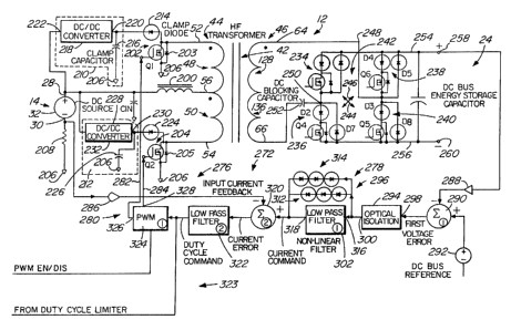
Referring back to Figure 1, the first DC to DC converter 12
further includes a first power control circuit shown
generally at 270, including a first inverter mode control
circuit 272 for controlling power flow from the first DC
port 14 to the DC bus 24, and a first charge mode control
circuit 274 for controlling power flow from the DC bus 24
to the first DC port 14.
First Inverter Mode Control Circuit
Referring to Figure 2, the first inverter mode control
circuit is shown generally at 272 and includes a current
CA 02216357 1997-09-23
-38-
control loop circuit 276 for generating a current feedback
signal responsive to current at the first DC port 14, a
voltage control loop circuit 278 for generating a current
command signal in response to DC bus voltage and a first
switching control circuit 280 for producing first and
second switching control signals 282 and 284 for
controlling the first and second switching elements 202 and
204 in response to the current feedback signal and the
current command signal.
The current control loop circuit 276 includes the current
sense resistor 208 connected between the second DC port
terminal 30 of the first DC port and the DC port signal
ground terminal 206, and a first signal conditioner 286 for
measuring the voltage across the current sense resistor 208
and for producing the current feedback signal such that the
current feedback signal has a voltage indicative of the
current drawn from the first DC source 32.
Voltage control loop
The voltage control loop circuit 278 includes a second
signal conditioner 288, a first subtracter 290, a DC bus
voltage reference source 292, a first optical isolator 294
and a first non-linear voltage loop compensation network
296.
The second signal conditioner 288 is connected to the
positive terminal 258 of the DC bus 24 for producing a DC
bus voltage feedback signal indicative of the voltage
appearing at the DC bus 24. The second signal conditioner
288 thus acts as a DC bus voltage feedback signal generator
for generating a DC bus voltage feedback signal indicative
of the DC bus voltage.
The DC bus voltage reference source 292 produces a DC bus
voltage reference signal. In this embodiment, this signal
CA 02216357 1997-09-23
-39-
is produced by a first reference voltage generator circuit
which generates a voltage of about 5 volts.
The first subtracter 290 is connected to the second signal
conditioner 288 and to the DC bus voltage reference source
292 and subtracts the DC bus voltage reference signal from
the DC bus voltage feedback signal to produce a first
voltage error signal. The first subtracter 290 is
connected to an input 298 of the first isolator 294. The
first isolator 294 also has an output 300 which is
connected to the first non-linear voltage loop compensation
network 296. The input 298 of the first isolator 294 is
referenced to the negative terminal 260 of the DC bus 24
while the output 300 of the first isolator 294 is
referenced to the DC port signal ground terminal 206. The
first isolator 294 thus provides electrical isolation
between components of the voltage control loop circuit 278
referenced to the negative terminal 260 and the components
of the current control loop circuit 276 referenced to the
DC port signal ground terminal 260. In effect therefore,
the first inverter mode control circuit 272 has a first
circuit portion connected to the primary winding and a
second circuit portion connected to the DC bus, and a first
isolator for electrically isolating the first circuit
portion from the second circuit portion while providing for
communication between the first and second circuit
portions.
The first isolator 294 effectively transmits the first
voltage error signal from the DC bus side of the apparatus
to the DC port side thereof. Thus, the first voltage error
signal is communicated via the isolator to the first non-
linear voltage loop compensation network 296.
The first non-linear voltage loop compensation circuit 296
includes a first low pass filter 302 and first and second
signal diode branches 312 and 314, each including three
CA 02216357 1997-09-23
-40-
signal diodes connected in series, the branches being
connected in parallel between an input 316 and an output
318 of the first low pass filter 302. Overall, the first
non-linear voltage loop compensation network 296 produces
the current command signal in response to the first voltage
error signal.
The first low pass filter 302 has a cutoff frequency of
about 5Hz which significantly reduces any 120Hz ripple
component in the first voltage error signal. The first low
pass filter 302 however has a relatively slow response time
in producing a change in the current command signal in
response to changes in the first voltage error signal. The
first branch 312, however, is operable to forward conduct
when the first voltage error signal changes at a rate at
which an instantaneous voltage drop across the first low
pass filter 302 exceeds a pre-defined value, in this
embodiment about 1.8 volts the pre-defined value being set
by the sum of the forward conducting voltage drops of each
diode in the branch. Similarly, the second branch 314 is
operable to forward conduct when the first voltage error
signal changes at a rate at which an instantaneous voltage
drop across the first low pass filter 302 exceeds a pre-
defined value, also about 1.8 volts, the pre-defined value
also being set by the sum of the forward conducting drops
of each diode in the branch. The first and second branches
312 and 314 are connected in opposing orientations and
therefore, the first branch 312 handles fast transitions in
the first voltage error signal of a first polarity while
the second branch 314 handles fast transitions of a
polarity opposite to the first polarity. Thus, the first
non-linear voltage loop compensation network 296 has a
relatively slow response in changing the current command
signal when the magnitude of the voltage across the first
low pass filter is within a first range, ie. 0 - 1.8 volts,
and has a relatively fast response in changing the current
CA 02216357 1997-09-23
-41-
command signal when the voltage across the first low pass
filter is within a second range, ie. above 1.8 volts.
Thus, the first low pass filter 302, and first and second
diode branches 312 and 314 act as a first non-linear
voltage loop compensation network 296 responsive to the DC
bus feedback signal for producing the current command
signal. This significantly reduces ripple which could
otherwise appear at the first DC source.
First switching control circuit
The first switching control circuit 280 includes a second
subtracter 320 for subtracting the current feedback signal
from the current command signal to produce a first current
error signal, a second low pass filter 322 for filtering
the first current error signal to produce a first duty
cycle command signal, a duty cycle limiter shown generally
at 323 and a first pulse width modulator circuit 324 having
first and second outputs 326 and 328 connected to the first
and second switching elements 202 and 204 for producing
first and second switching signals for controlling the
first and second switching elements 202 and 204.
Duty cycle limiter
Referring to Figure 2a, the duty cycle limiter includes a
an open collector voltage follower 327 having an input 329
connected to a common terminal 331 of an analog switch 333
and an output 325 connected to the second low pass filter
(not shown) for receiving the duty cycle command signal
therefrom. The analog switch has a first input 335 for
receiving a signal proportional to the voltage of the DC
source (32), through a buffer 337. The analog switch
further has a second input 339 for receiving a running duty
cycle limit setpoint voltage from a setpoint voltage
network 341.
CA 02216357 1997-09-23
-42-
The setpoint voltage network 341 includes first and second
resistors 343 and 345 which act as a voltage divider, with
the input 339 of the analog switch 333 being connected
between the first and second resistors 343 and 345.
A voltage reference signal is provided by a voltage
reference generator (not shown), the voltage reference
signal having a voltage of approximately 6.8 volts, is
provided to the first resistor 343.
Also connected between the first and second resistors 343
and 345 are a 30 percent control circuit 347, a 55 percent
control circuit 391 and a 0 percent control circuit 349
respectively.
The 30 percent control circuit 347 includes a diode 355, a
resistor 357 and a transistor 359 connected in series. The
transistor 359 has a first base 361 to which is connected
an OR gate 365 having first and second inputs 367 and 369
to which are connected first and second comparators 371 and
373. The first and second comparators are for comparing
the DC bus voltage sense signal with high and low reference
signals respectively. If the DC bus voltage sense signal
is greater than the high level reference signal which, in
this embodiment represents 225 volts, the first comparator
371 renders its output active which turns on the first
transistor thereby rendering operational, the 30 percent
control circuit 347. Alternatively, if the DC bus voltage
sense signal is less than the low level reference signal
which, in this embodiment, represents 125 volts, the second
comparator 373 renders its output active which also turns
on the first transistor 359, also rendering the 30 percent
control circuit 347 operational.
The 55 percent control circuit includes a diode 395, a
resistor 401, a transistor 405 and a comparator 381
connected in series. The comparator compares the voltage
CA 02216357 1997-09-23
-43-
appearing at at least one of the clamp circuits (210 and
212 shown in Figure 2) with a high clamp voltage reference
voltage signal. When the clamp voltage is higher than the
high clamp reference voltage, which in this embodiment
represents 55 volts, comparator 381 renders its output
active thereby turning on the transistor 405 and rendering
operational the 55 percent control circuit 391.
Similarly, the 0 percent control circuit includes a diode
397, a resistor 403, a transistor 407 and a comparator 383
connected in series. The comparator compares the voltage
appearing at at least one of the clamp circuits (210 and
212 shown in Figure 2) with a low clamp voltage reference
voltage signal. When the clamp voltage is lower than the
low clamp reference voltage, which in this embodiment
represents 5 volts, comparator 383 renders its output
active thereby turning on the transistor 407 and rendering
operational the 0 percent control circuit 349.
Thus, when the DC bus voltage sense signal is within its
associated high and low reference signals, and when the
clamp voltage is within its high and low reference signals,
neither the 30 percent, the 55 percent nor the 0 percent
control circuits 347, 391 or 349 are rendered operational
in which case, only the resistors 343 and 345 act to set a
duty cycle limit value, and in this embodiment, this value
represents an 80 percent duty cycle.
The analog switch 333 further includes a selection input
351 to which is connected a signal line for providing a PWM
enable/disable signal from the microprocessor (not shown),
for controlling the connection of the common terminal 331
to the first and second inputs 335 and 339 respectively.
In the enable position, the common terminal 331 is
connected to the second input 339 and in the disable
position, the common terminal 331 is connected to the first
input 335.
CA 02216357 1997-09-23
-44-
The effect of the duty cycle limiter is to limit the
voltage of the first duty cycle command signal appearing at
the output of the low pass filter such that the signal is
unable to attain a voltage greater than a value
representing 80 percent, 55 percent, 30 percent or 0
percent duty cycle, depending upon the voltage at the DC
bus and the voltage at the clamp circuits.
First pulse width modulator
Referring to Figure 6, the first pulse width modulator
circuit 324 includes first and second waveform generators
330 and 332 for generating first and second pulse width
modulated waveforms 180 degrees out of phase with each
other. The first waveform generator 330 includes a
triangle wave generator 334, and a first comparator 336.
The second waveform generator 332 includes the triangle
wave generator 334, an inverter 340, and a second
comparator 342.
The triangle wave generator 334 has an output 354 which is
connected to the inverter 340 and to the non-inverting
input 356 of the first comparator 336. The inverter 340
has an output which is connected to the non-inverting input
358 of the second comparator 342. The first and second
comparators 336 and 342 thus receive at their respective
non-inverting inputs 356 and 358 first and second triangle
waveforms 180 degrees out-of-phase with each other and
receive at their inverting inputs 350 and 352 the first
duty cycle command signal. The first and second
comparators 336 and 342 have respective first and second
outputs 326 and 328 which produce first and second square
wave signals respectively 180 degrees out-of-phase with
each other. Each square wave signal has respective
cyclicly occurring on and off states with a cyclic
frequency of approximately 60kHz, and each square wave
signal has a respective duty cycle. Therefore, the duty
CA 02216357 1997-09-23
-45-
cycles of the first and second square wave signals are
varied in response to the first duty cycle command signal.
Referring back to Figure 2, the first and second square
wave signals are supplied to the first and second switching
elements 202 and 204 respectively to place the first and
second switching elements in conducting and non-conducting
modes according to the on and off states respectively, of
the first and second square wave signals respectively.
Thus, the first and second switching elements are placed in
conducting and non-conducting modes for periods of time
dependent on the first duty cycle command signal.
DC to DC converter inverter mode operation
Referring to Figure 2, in the inverter mode, current flows
from the first DC port terminal 28 through the input
inductor 200 and into the centre tap terminal 56 of the
primary winding 44 of the transformer 42. Current flow
through the first and second portions 48 and 50 of the
primary winding 44 is controlled by the first and second
switching elements 202 and 204. The first and second
switching elements 202 and 204 are switched at a high
frequency, by the first and second square wave signals from
the pulse width modulator circuit 324. The third, fourth,
fifth, and sixth switching elements 234, 236, 238 and 240
are inactive in the inverter mode. The diodes in series
with the third, fourth, fifth, and sixth switching elements
respectively, prevent conduction of current through the
MOSFETs, rather, current is conducted through the
associated parallel diodes (262 in Figure 5).
The first and second switching elements 202 and 204 are
operated in two modes, including an overlapping mode and a
non-overlapping mode. In the overlapping mode, either the
first switching element 202 or the second switching element
204 is in conduction or both the first and second switching
elements 202 and 204 are in conduction. When only the
CA 02216357 1997-09-23
-46-
first switching element 202 is in conduction, current flows
through the first portion 48 of the primary winding 44,
through the first switching element 202 and to the second
DC port terminal 30. At the bridge 242, current flows out
of the second primary winding terminal 66, through the DC
blocking capacitor 252 and through the third switching
element 234 to the positive terminal 258 of the DC bus 24.
Current returns from the negative terminal 260 of the DC
bus 24 through the sixth switching element 240 to the first
secondary winding terminal 64.
When only the second switching element 204 is in
conduction, current flows through the second portion 50 of
the primary winding 44, through the second switching
element 204 and to the second DC port terminal 30. Current
flows out of the first secondary winding terminal 64,
through the fifth switching element 238 to the positive
terminal 258 of the DC bus 24. Current returns from the
negative terminal 260 of the DC bus 24 through the fourth
switching element 236 and the DC blocking capacitor 252 to
the second secondary winding terminal 66.
When only the first or second switching element 202 and 204
is in conduction, energy is transferred from the input
inductor 200 and from the first DC port 14 to the DC bus
24. When both the first and second switching elements 202
and 204 are in conduction, current flows in both the first
and second portions of the primary winding 48 and 50,
through the first and second switching elements 202 and 204
to the second DC port terminal 30. Because the first and
second primary winding portions 48 and 50 are wound in
opposing directions, the current flows in opposing
directions and no net magnetic flux is produced in the
transformer 42. As a result, no voltage appears across the
secondary winding 46 of the transformer 42 and no energy is
transferred to the DC bus 24. In this mode, the input
inductor 200 is effectively connected across the first and
CA 02216357 1997-09-23
-47-
second DC port terminals 28 and 30 and current flowing
through the input inductor 200 increases, resulting in
increased energy stored in the input inductor 200. Thus,
by adjusting the ratio between the time that the first and
second switching elements 202 and 204 are both in
conduction mode, and the time during which only the first
or second switching element 202 and 204 is in conduction,
power balance and DC bus voltage regulation can be
achieved.
In the non-overlapping mode, either the first switching
element 202 is in conduction, the second switching element
204 is in conduction, or both the first and second
switching elements 202 and 204 are non-conducting. The
current flow when the first or second switching element 202
or 204 is on is essentially the same as described above
with respect to the overlapping mode. However, in the non-
overlapping mode, when either the first or second switching
element 202 or 204 is on, the voltage at the centre tap
terminal 56 of the primary winding 44 is lower than the
voltage of the first DC source 32. Thus, current in the
input inductor 200 increases and energy stored in the input
inductor increases while the first or second switching
element 202 or 204 is on even though energy is also
transferred to the DC bus 24. When both the first
switching element 202 and the second switching element 204
are off, inductor current flows in both the first and
second portions 48 and 50 of the primary winding, through
the first and second clamp diodes 214 and 224 and into the
first and second clamp capacitors 216 and 226 respectively.
As the first and second winding portions 48 and 50 of the
primary winding 44 are wound in opposing directions, the
current flows in opposing directions and no net magnetic
flux is produced in the transformer 42. Therefore, no
voltage appears across the secondary winding 46 and
therefore no energy is transferred to the DC bus 24.
However, the voltage across the first and second clamp
CA 02216357 1997-09-23
-48-
capacitors 216 and 226 is more than twice the source
voltage, and therefore, energy is transferred from the
first and second clamp capacitors 216 and 226 back to the
first DC source 32 by the second and third DC to DC
converters 218 and 228. As a result, current in the input
inductor 200 decreases and energy is transferred from the
input inductor 200 back to the first DC source 32. This
eliminates the need for a clamp winding normally used on
such inductors.
The first and second clamping circuits 210 and 212 also act
to absorb energy stored in the leakage inductance of the
transformer 42 in both operating modes, eliminating
potentially damaging voltage transients across the first
and second switching elements 202 and 204 when they are
switched from conducting mode to non-conducting mode.
As mentioned above, the transformer turns ratio is selected
so that when the DC bus 24 is at its nominal voltage, the
reflected voltage at the centre tap terminal 56 is higher
than the highest DC source voltage anticipated. This
ensures that the DC to DC converter 12 usually operates in
overlap mode. Non-overlap mode operation occurs when the
DC bus 24 is lightly loaded or is being charged to its
nominal operating voltage.
Control circuit
As discussed above, the first and second switching elements
202 and 204 are normally operated in the overlapping mode
and by adjusting the ratio between the time that the first
and second switching elements 202 and 204 are both in
conduction and the time that only the first or second
switching element 202 or 204 is in conduction, power
balance and DC bus voltage regulation can be achieved.
These ratios are controlled by the pulse width modulator
circuit 324 in response to the first duty cycle command
signal. The first duty cycle command signal is a filtered
CA 02216357 1997-09-23
-49-
version of the first current error signal which is produced
from the input current feedback signal and the current
command signal. The current command signal is effectively
set by the DC bus voltage as indicated by the DC bus
voltage feedback signal. As the DC bus voltage decreases
due to loading, the voltage error signal increases. A
gradual increase in DC bus loading will result in a gradual
increase in the voltage error signal. The voltage error
signal is effectively filtered by the first low pass filter
302 to produce the current command signal and the current
command signal is effectively diminished by the input
current feedback signal to produce the first current error
signal. This decreases the duty cycles of the first and
second square waveforms which reduces the period of time
during which both the first and second switching elements
202 and 204 are in conduction, and increases the period of
time during which one of the switching elements is on and
the other is off.
In the event that a load is placed abruptly on the DC bus
24, the DC bus voltage decreases rapidly and therefore the
voltage error signal rises rapidly. The low pass filter
output 318 does not rise as rapidly as the voltage error
signal, and therefore, a voltage drop appears across the
first low pass filter 302. If this drop is sufficient to
place the first or second signal diodes 304 and 306 into
conduction, ie. above 1.8 volts, the rapid increase in
voltage error signal also appears as a rapid increase in
the current command signal due to the first non-linear
voltage loop compensation network. Thus, the first current
error signal changes rapidly, as does the first duty cycle
command signal which causes a rapid change in the duty
cycles of the first and second square wave signals. Thus,
during normal operation, the duty cycles of the first and
second square wave signals are adjusted rather smoothly as
the load at the DC bus 24 changes slowly, however, when the
load at the DC bus changes abruptly, an immediate response
CA 02216357 1997-09-23
-50-
is seen in the duty cycles of the first and second square
wave signals. Thus, the inverter mode control circuit 272
provides for tight regulation of the DC to DC converter 12
over a wide range of loads.
In the inverter mode of operation an advantage of the duty
cycle limiter 323 used in this embodiment is that the duty
cycle of the first and second switching elements 202 and
204 is limited to prevent a 100 percent duty cycle
condition from occurring, which would cause the converter
to self-destruct. Under normal operating conditions, the
first duty cycle command signal is limited by the duty
cycle limiter to limit the duty cycle to about 80 percent.
When the converter is changed from overlapping mode to
non-overlapping mode, the clamp voltage is excessive, which
enables the 55 percent control circuit 349 so that the duty
cycle is limited to about 55 percent to make the voltage
appearing at the secondary winding 46 less than the voltage
at the DC bus 24, which reduces input current to zero.
When the device is started, the DC bus voltage is zero and
increasing during which time the first control circuit is
enabled, which limits the duty cycle to about 30 percent
limiting the input current to a few amperes or less, for a
soft-start. After the DC bus voltage exceeds the low
reference value, the 30 percent control circuit 347 is
disabled and the duty cycle is limited to 80 percent as
described above . If the DC bus voltage exceeds the high
reference value, the 30 percent control circuit 347 is re
enabled, which again limits the duty cycle to 30 percent,
to prevent excess voltage at the DC bus.
Basically, the first inverter mode control circuit is
operable to control the DC to DC converter as a push-pull,
current-fed transformer-isolated boost step-up converter.
First charge mode control circuit
CA 02216357 1997-09-23
-51-
Referring to Figure 7, the first charge mode control
circuit includes a second switching control circuit 360
having first and second outputs 362 and 364 in
communication with the third, fourth fifth and sixth
switching elements 234, 236, 238 and 240, for controlling
conduction of the third, fourth, fifth and sixth switching
elements to produce a high frequency voltage waveform
across the secondary winding 46 when power is supplied to
the DC bus 24 by the DC/AC converter 18 operating in
charging mode.
The second switching control circuit 360 includes a bridge
current command signal generator 366 for producing a bridge
current command signal in response to voltage and current
at the first DC port 14 and a bridge current feedback
signal generator 368 for producing a bridge current
feedback signal in response to current drawn at the second
DC port, a third subtracter 370 for subtracting the bridge
current feedback signal from the bridge current command
signal to produce a second duty cycle command signal, and
a second pulse width modulator 372 responsive to the second
duty cycle command signal for producing third, fourth,
fifth and sixth switching signals operable to control
switching of the third, fourth, fifth and sixth switching
elements 234, 236, 238 and 240.
Bridcre current feedback sicrnal generator
The bridge current feedback signal generator 368 includes
first and second low resistance current sense resistors 374
and 376, a summer 378 and a third low pass filter 380. The
first and second current sense resistors 374 and 376 are
connected in series with the fourth switching element 236
and the sixth switching element 240 respectively and the
negative terminal 260. The first and second current sense
resistors 374 and 376 act as signal generators for
generating first and second current sense signals
CA 02216357 1997-09-23
-52-
respectively, representing current flow in the fourth and
sixth switching elements 236 and 240 respectively.
The first and second current sense signals are provided to
the summer 378 which sums them together to produce a raw
bridge current feedback signal. The raw bridge current
feedback signal is provided to the third low pass filter
380 which filters the raw bridge current feedback signal to
produce the bridge current feedback signal. The bridge
current feedback signal has a voltage level which increases
with an increase in current through either or both of the
first and second current sense resistors 374 and 376 and
which decreases with a decrease in current through either
of the first and second current sense resistors.
Bridge current command si n~generator
The bridge current command signal generator 366 includes a
second current error signal generator 382, a voltage error
signal generator 384, a signal selector circuit 386 and an
isolator 388.
Second current error signal Generator
The second current error signal generator 382 generates a
second current error signal in response to current flow at
the first DC port 14. The second current error signal
generator 382 includes a charging current signal generator
390 for generating a charging current signal indicative of
current at the first DC port 14, a fourth low pass filter
392 for filtering the charging current signal to produce a
filtered charging current signal, a charge current command
signal generator 394 for generating a charge current
command signal indicative of a desired charging current and
a fourth subtracter 396 for subtracting the filtered
charging current signal from the charge current command
signal to produce the second current error signal.
CA 02216357 1997-09-23
-53-
The charging current signal generator 390 includes the
current sense resistor 208 connected to the first DC source
32 and a signal conditioner 398 connected to the current
sense resistor for producing the charging current signal.
The charging current signal has a voltage level indicative
of the current flowing in the current sense resistor 208,
that is, the current flowing to the first DC source 32.
The fourth low pass filter 392 has a cutoff frequency of
approximately OHz and filters the charging current signal
to produce a filtered charging current signal.
The charge current command signal generator 394 includes
the microprocessor (not shown) and a first digital to
analog converter (not shown), operable to receive a digital
code from the microprocessor indicative of a desired charge
current set by a pre-defined charging schedule and to
produce a charge current command signal having a voltage
level indicative of the desired charge current. Different
charging schedules may be used depending upon the type or
capacity of DC source employed or the power rating of the
AC source. For example, a different charging schedule is
employed for a wet cell battery as compared to the charging
schedule employed for a gel cell battery.
The fourth subtracter 396 simply subtracts the voltage
level of the filtered charging current signal from the
voltage level of the charge current command signal to
produce the second current error signal having a voltage
level indicative of the difference between the charge
current command signal and the filtered charging current
signal.
Voltage error signal generator
The voltage error signal generator 384 includes a charging
voltage signal generator 400, a charging voltage reference
CA 02216357 1997-09-23
-54-
signal generator 402, a fifth subtracter 404 and a second
non-linear voltage loop compensation network 406.
The charging voltage signal generator 400 includes a signal
conditioner 408 connected to the first DC port terminal 28
for generating a charging voltage signal having a voltage
level indicative of voltage at the first DC port 14.
The charging voltage reference signal generator 402
includes the microprocessor (not shown) and a second
digital to analog converter (not shown) for generating a
charging voltage reference signal indicative of a desired
charging voltage. The microprocessor provides a digital
code to the second digital to analog converter, the digital
code representing a desired voltage according to the pre-
defined charging schedule and type and temperature of the
DC source.
The fifth subtracter 404 subtracts the charging voltage
signal from the charging voltage reference signal to
produce a raw voltage error signal. The raw voltage error
signal is provided to the second non-linear voltage loop
compensation network 406 which filters the raw voltage
error signal to produce the second voltage error signal.
The second non-linear voltage loop compensation network 406
includes a fifth low pass filter 410 and a third signal
diode 412. The third signal diode 412 is connected in
parallel between an input 416 and an output 418 of the
fifth low pass filter 410. Overall, the second non-linear
voltage loop compensation network 406 produces the second
voltage error signal in response to the raw voltage error
signal.
The fifth low pass filter 410 has a cutoff frequency of 0
Hz and a relatively slow response time in producing a
change in the second voltage error signal in response to
CA 02216357 1997-09-23
-55-
the charging voltage signal. The third signal diode 412 is
operable to forward conduct when the raw voltage error
signal changes at a rate at which an instantaneous voltage
drop across the fifth low pass filter 410 exceeds a pre-
y defined value, in this embodiment 0.2 volts, the pre-
defined value being set by the voltage drop across the
diode when forward conducting. Thus, the second non-linear
voltage loop compensation network 406 has a relatively slow
response in changing the second voltage error signal when
the voltage across the fifth low pass filter is within a
first range, ie. 0 - 0.2 volts and has a relatively fast
response in changing the second voltage error signal when
the voltage across the fifth low pass filter is within a
second range, (ie. > 0.2 volts) corresponding to a slew
rate of about 12.6 v/sec., rising only.) In other words,
the second non-linear voltage loop compensation network 406
is operable to provide a slow response when the voltage
across the fifth low pass filter is relatively small and a
fast response when the voltage across the fifth low pass
filter is relatively large.
Signal selector
The signal selector 386 has first and second inputs 420 and
422 for receiving the second current error signal and the
second voltage error signal and has an output 438 for
producing a lesser output signal responsive to the lesser
of the second current error signal and the second voltage
error signal.
Figure 8
Referring to Figure 8, the first and second inputs 420 and
422 are connected to first and second resistors 424 and 426
respectively. The first resistor 424 is connected to a
second diode 428 which is connected to the base 430 of a
signal transistor 432. The second resistor 426 is also
connected to the base 430 of the signal transistor 432.
CA 02216357 1997-09-23
-56-
The signal transistor 432 has a collector terminal 433
connected to a 12 volt supply and has an emitter terminal
434 to which is connected a current limiting resistor 436.
The current limiting resistor has a connection to the
second isolator 388. This connection acts as the output
438 of the signal selector 386. The lesser output signal
appears at the output 438.
The second isolator 388 has an input 440 for receiving the
lesser output signal and has an output 442 for producing a
bridge current command signal. The input 440 is
electrically connected to the first DC port through the DC
port signal ground terminal 206. The output is
electrically connected to the DC bus 24 through the DC bus
negative terminal 260. The input 440 and the output 442
are electrically isolated from each other and the input 440
is referenced to the DC port signal ground terminal 206 and
the output 442 is referenced to the DC bus negative
terminal 260. Thus the second isolator 388 passes the
lesser output signal from circuit components referenced to
the DC port to circuit components referenced to the DC bus
of the apparatus, without any electrical connection between
the DC bus and the DC port. The lesser output signal as it
appears at the output of the second isolator 388 acts as
the bridge current command signal.
Referring back to Figure 7, the third subtracter 370
subtracts the bridge current feedback signal from the
bridge current command signal to produce the second duty
cycle command signal. The second duty cycle command signal
is provided to the second pulse width modulator 372 which,
in this embodiment includes a 3525A pulse width modulator
control circuit available from Motorola Inc.
Referring to Figure 9, the second pulse width modulator 372
has an Rt input 446, a Ct input 447, a COMP input 448, an
inverting input 449, a non-inverting input 451 and a first
CA 02216357 1997-09-23
-57-
output stage 450 having first and second outputs A (362)
and B (364). A resistor and capacitor are connected to the
Rt and Ct inputs 446 and 447 to cause an oscillator in the
circuit to have a frequency of about 60kHz. The COMP input
448 is connected to the inverting input 449 and the second
duty cycle command signal is provided to the non-inverting
input 451. The first and second outputs 362 and 364 are
connected to a switch driver (HARRIS HIP2500) (not shown)
and the switch driver is connected to first and second
pairs of switching elements. Referring back to Figure 7,
in this embodiment, the first pair includes the third and
sixth switching elements 234 and 240 and the second pair
includes the fourth and fifth switching elements 236 and
238. Thus, the first output 362 is connected to and is
operable to simultaneously control the third and sixth
switching elements 234 and 240 and the second output 364 is
connected to and is operable to simultaneously control the
fourth and fifth switching elements 236 and 238. Thus, the
first output 362 produces third and sixth switching element
control signals, which are actually the same signal
hereinafter referred to as the third/sixth switching
element control signal and the second output produces
fourth and fifth switching element control signals, which
are actually the same signal, hereinafter referred to as
the fourth/fifth switching element control signal.
The third/sixth switching element control signal and the
fourth/fifth switching element control signal are cyclic,
having high and low states at a frequency of approximately
60kHz and a variable duty cycle. The duty cycle changes in
response to changes in the second duty cycle command
signal. The high state represents a relatively high
voltage level and is used to turn on or place in a
conduction mode the switching elements receiving the
signal, while the low state represents a relatively low
voltage level and is used to turn off or place in a non-
CA 02216357 1997-09-23
-58-
conducting mode the switching elements receiving the
signal.
Examples of the signals produced at the first and second
outputs 362 and 364, in response to the second duty cycle
command signal are shown in Figure 10. As the second duty
cycle command signal increases, the duty cycles of the
third/sixth switching element control signal and the
fourth/fifth switching element control signal are
increased. Thus, as the second duty cycle command voltage
is increased, the third and sixth switching elements (234
and 240) and also the fourth and fifth switching elements
236 and 238 remain in the conducting mode for a longer
period of time.
Referring back to Figure 7, as the second duty cycle
command signal is increased or decreased in response to the
bridge current feedback signal and the bridge current
command signal, the second pulse width modulator 372, third
subtracter 370 and voltage error signal generator 384 and
second current error signal generator 382 act as a
switching signal generator for generating third, fourth,
fifth and sixth switching element control signals
responsive to voltage or current at the first DC port 14
and current at the second DC port 16, the third, fourth,
fifth and sixth switching signals being operable to place
the third, fourth, fifth and sixth switching elements 234,
246, 238 and 240 in conducting and non-conducting states.
Operation of DC to DC converter in charqer mode
In the charger mode, the third, fourth, fifth, sixth
switching elements 234, 236, 238 and 240 are active while
the first and second switching elements 202 and 204 are
inactive (always off). Switching of the third, fourth,
fifth and sixth switching elements is controlled so that
the switches are always in one of three configurations as
follows
CA 02216357 1997-09-23
-59-
Configuration 1 - third switching element 234 and sixth
switching element 240 on, the fourth and fifth switching
elements 236 and 238 off;
Configuration 2 - All switching elements off;
Configuration 3 - The third and sixth switching elements
234 and 240 off and the fourth and fifth switching elements
236 and 238 on;
By sequenc ing through Conf igurat ion 1, Conf igurat ion 2 , and
Configuration 3 at a high frequency, a voltage waveform as
shown in Figure 11 is applied to the secondary winding of
the transformer. Referring to Figure 7, this high
frequency alternating voltage is stepped down by the
transformer 42 and appears at the primary winding terminals
52 and 54. The anti-parallel diodes 203 and 205 in the
first and second switching elements 202 and 204 act as a
centre tapped rectifier circuit to rectify the transformer
voltage so that a DC voltage is applied to the input
inductor 200. The anti-parallel diodes 203 and 205 in the
low voltage MOSFETs used in the first and second switching
elements 202 and 204 have fast recovery characteristics.
When the third, fourth, fifth and sixth switching elements
234, 236, 238 and 240 are in Configuration l, current flows
from the positive terminal 258 of the DC bus 24 through the
third switching element 234, through the blocking diode and
through the DC blocking capacitor 252 into the second
secondary winding terminal 66. Current flows out of the
first secondary winding terminal 64 of the secondary
winding 46, through the blocking diode associated with the
sixth switching element 240 and through the sense resistor
376 to the negative terminal 260 of the DC bus 24.
On the first DC port side of the transformer 42, current
flows from the second DC port terminal 30 of the first DC
CA 02216357 1997-09-23
-60-
port, through the anti-parallel diode 203 in the first
switching element 202 and into the first primary winding
terminal 52 of the primary winding 44 of the transformer
42. Current flows out of the centre tap terminal 56,
through the input inductor 200 and out the first DC port
terminal 28. As the transformer turns ratio has been
chosen such that the voltage at the centre tapped terminal
is higher than the voltage at the DC port positive terminal
when the apparatus is in use, current flowing through the
input inductor 200 increases and energy is stored in the
input inductor 200.
When the third, fourth, fifth and sixth switching elements
234, 236, 238 and 240 are placed in Configuration 2, (all
off) no voltage is applied to the secondary winding 46 of
the transformer. It will be appreciated that alternative
switch configurations such as the third switching element
234 and fifth switching element 238 on and the fourth and
sixth switching elements 236 and 240 off, will achieve the
same effect.
In the second configuration, on the DC port side of the
transformer 42, the input inductor 200 maintains current
flow to the first DC port 14. Current flows from the
negative terminal of the first DC port terminal 30 through
the anti-parallel diodes 203 and 205 in the first and
second switching elements 202 and 204, into the first and
second primary winding terminals 52 and 54 and out of the
centre tap terminal 56 and through the input inductor 200
to the first DC port terminal 28 of the first DC port 14.
In this case, the voltage at the centre tap terminal 56 is
less than the voltage at the first DC port terminal 28 of
the first DC port 14. Therefore, current flowing through
the input inductor 200 decreases and energy is supplied to
the source by the input inductor 200.
CA 02216357 1997-09-23
-61-
When the third, fourth, fifth and sixth switching elements
234, 236, 238 and 240 are in Configuration 3, current flows
from the positive terminal 258 of the DC bus 24 through the
fifth switching element 238 and its associated blocking
diode, into the first secondary winding terminal 64.
Current flows out of the second secondary winding terminal
66, through the DC blocking capacitor 252, through the
fourth switching element 236 and its associated blocking
diode, through sense resistor 374, to the negative terminal
260 of the DC bus 24. On the first DC port side of the
transformer, current flows from the second DC port terminal
30 of the first DC port 14, through the anti-parallel diode
205 in the second switching element 204 and into the second
primary winding terminal 54. Current flows out of the
centre tap terminal 56 of the primary winding, through the
input inductor 200 and out the first DC port terminal 28 of
the first DC port 14.
The first and second clamping circuits 210 and 212 are also
active in the charger mode, limiting voltage transients
across the first and second switching elements 202 and 204.
Output current and voltage appearing at the first DC port
14 are regulated by varying the duty cycle of the voltage
appearing at the centre tap terminal 56 of the transformer,
which in turn is controlled by the duty cycle of the
third/sixth and fourth/fifth switching element control
signals produced at outputs 362 and 364 the second pulse
width modulator 372.
Effectively, in the charging mode, the microprocessor (not
shown) sends codes to the first and second digital to
analog converters respectively which provide charge current
command and charge voltage command signals accordingly, to
the fourth and fifth subtracters 396 and 404 respectively
in accordance with the pre-defined charging schedule. The
fourth and fifth subtracters 396 and 404 subtract the
CA 02216357 1997-09-23
-62-
charging current signal representing the charge current
supplied to the source and the voltage feedback signal
representing voltage at the source, respectively from the
charge current command signal and the charge voltage
command signal respectively, to produce the second current
error signal and the voltage error signal respectively.
The voltage error signal is passed through the second
voltage loop compensation network 406 to produce the second
voltage error signal. The second voltage loop compensation
network 406 provides a slow voltage loop response when the
voltage error signal is relatively small and a fast voltage
loop response when the voltage error signal is relatively
large. The second voltage error signal produced by the
second voltage loop compensation network and the second
current error signal, are provided to the signal selector
386 which presents at its output, the lesser value of the
second current error signal and the second voltage error
signal. This has the effect of ensuring that neither the
output voltage nor the output current will exceed its
commanded value, as dictated by the microprocessor. If
achieving the output voltage commanded would require an
output current greater than that commanded, then the
current command will dominate. Conversely, if achieving
the output current commanded would require an output
voltage greater than that commanded, then the voltage
command will dominate.
As described above, an increase in the second duty cycle
command signal increases the duty cycle of the third/sixth
switching element control signal at output 362 and an
increase in the duty cycle of the fourth/fifth switching
element control signal at output 364, thereby increasing
the duration of time during which the switching elements
are in conduction, and increasing power transfer from the
DC bus 24 to the first DC port 14. Similarly, a decrease
in the second duty cycle command signal decreases the time
during which the third, fourth, fifth and sixth switching
CA 02216357 1997-09-23
-63-
elements are in conduction, thereby reducing the duration
of time during which the switching elements are in
conduction, and decreasing power transfer from the DC bus
24 to the first DC port 14.
It will be appreciated that the first charge mode control
circuit is operable to control the DC to DC converter 12 as
a full-bridge voltage fed transformer-isolated buck step-
down converter with centre tapped output rectifiers.
DC Bus
Referring back to Figure 1, in this embodiment, the DC bus
is formed from a pair of copper circuit board traces (not
shown) to which the second DC port 16 and third DC port 20
are connected. The load balancing energy storage element
26 includes eight 470uF 250 volts capacitors shown
generally at 456, connected between the positive terminal
258 and the DC bus negative terminal 260. The capacitors
decouple the DC to DC converter 12 from the DC to AC
converter 18 by supplying energy to the DC bus 24 when a
voltage at the DC bus 24 is decreasing and by storing
energy received from the DC bus 24 when a voltage at the DC
bus 24 is increasing. This enables the apparatus to receive
power from the first DC source 32 and supply power to the
first DC source 32 substantially ripple free even though
power supplied to and received from the AC port has a
ripple at twice the frequency of the AC voltage.
DC to AC Converter
Referring to Figure 3, the DC to AC converter 18 includes
a full bridge converter 470 and an AC output low pass
filter 472. The full bridge converter 470 includes seventh
474, eighth 476, ninth 478 and tenth 480 switching elements
connected to the DC bus 24 in a full bridge topology having
first and second bridge input terminals 482 and 484
connected to the DC bus 24 and first and second bridge
output terminals 486 and 488 connected to the AC output low
CA 02216357 1997-09-23
-64-
pass filter 472. Effectively, the bridge output terminals
486 and 488 provide a pulse width modulated waveform to the
AC output low pass filter 472. In this embodiment, each of
the seventh 474, eighth 476, ninth 478 and tenth 480
switching elements includes four paralleled IRF646 N-
channel Power MOSFETs manufactured by Harris Corporation of
the United States.
The AC output low pass filter 472 has an input 490
connected to the full bridge output terminals 486 and 488
for receiving the pulse width modulated waveform and has a
filter output 492 to which is connected an electromagnetic
interference filter 494 having AC in/out line and neutral
terminals 34 and 36 which act as the AC port 22. The AC
output low pass filter 472 includes first and second 600uH
filter inductors 496 and 498, third and fourth 40 uH filter
inductors 500 and 502, and first and second filter
capacitors 504 and 506. The first and third filter
inductors 496 and 500 are connected in series with the
second bridge output terminal 488 and the second and fourth
filter inductors 498 and 502 are connected in series with
the first bridge output terminal 486.
The DC to AC converter 18 further includes a snubber
circuit shown generally at 508 connected between the bridge
output terminals 486 and 488 and the DC bus 24. The
snubber circuit 508 includes eleventh 510 and twelfth 512
switching elements connected to the bridge output terminals
486 and 488 first and second snubber diodes 514 and 516
connected in parallel with the eleventh 510 and twelfth 512
switching elements respectively and second and third
inductors 518 and 520 connected to the eleventh 510 and
twelfth 512 switching elements respectively and connected
to each other and to a third snubber diode 522 connected to
the second and third inductors 518 and 520 and the DC bus
24. In this embodiment, each of the eleventh and twelfth
switching elements 510 and 512 includes a single
CA 02216357 1997-09-23
-65-
HGTP20N60B3 40A, 600 volts UFS Series N-channel IGBT
manufactured by Harris Corporation.
Referring to Figure 1, the DC to AC converter 18 further
includes a second power control circuit 524 which operates
independently of the first power control circuit 270
controlling the DC to DC converter 12. The second power
control circuit 524 includes an inverter mode control
circuit 526 for generating an inverter mode current command
signal, a charge mode control circuit 528 for generating a
charge mode current command signal and a third switching
control circuit 530 for controlling the seventh, eighth,
ninth, tenth, eleventh, and twelfth switching elements in
the inverter mode and in the charge mode respectively, in
response to the inverter mode command signal and the charge
mode command signal respectively.
Inverter Mode Control Circuit
Referring back to Figure 3, the inverter mode control
circuit 526 acts as an inverter mode current command signal
generator and includes an AC output voltage control circuit
527 and a DC offset correction circuit 532 for producing
and varying the inverter mode current command signal in
response to AC output voltage and DC offset voltage
measured across capacitor 504.
The AC output voltage control circuit 527 includes an AC
output voltage sense signal generator 534 connected to a
circuit node between the first and third filter inductors
496 and 500.
The AC output voltage sense signal generator 534 includes
a first signal conditioner 544 connected to a circuit node
between the first and third filter inductors 496 and 500 to
produce an AC output voltage sense signal responsive to AC
voltage at the bridge output terminals 486 and 488.
CA 02216357 1997-09-23
-66-
The DC offset correction circuit 532 includes a sixth low
pass filter 536, a sinewave reference signal generator 538,
a sixth subtracter 540 and a seventh subtracter 542. The
sixth low pass filter 536 receives the AC output voltage
sense signal and produces a filtered DC offset signal in
response to the AC output voltage sense signal.
The sinewave reference signal generator 538 includes the
microprocessor (not shown). The microprocessor sends a
sinusoidally width modulated digital pulse train to a
filter (not shown) which produces the desired sinewave
reference signal. The pulse train may represent an AC
waveform having a frequency of 50Hz or 60Hz, as desired.
In response, the filter produces a sinewave reference
signal, at the desired frequency.
A sixth subtracter 540 subtracts the filtered DC offset
signal from the sinewave reference signal to produce an
output voltage command signal.
A seventh subtracter 542 subtracts the AC output voltage
sense signal from the output voltage command signal to
produce the inverter mode current command signal. Thus,
the inverter mode current command signal is produced and
varied in response to both the AC output voltage and the DC
offset voltage.
Charge Mode Command Signal Generator
Referring to Figure 12, the charge mode control circuit 528
includes a DC bus voltage sense signal generator 546, a DC
bus voltage reference signal generator 548, a current
waveform signal generator 550, an eighth subtracter 551,
and a multiplier 552.
The DC bus voltage sense signal generator 546 includes a
second signal conditioner 554 connected to the positive
CA 02216357 1997-09-23
-67-
terminal 258 of the DC bus 24, for producing a DC bus
voltage sense signal responsive to voltage at the DC bus.
The DC bus voltage reference signal generator 548 includes
an analog voltage reference integrated circuit, in this
embodiment a TL431 available from Texas Instruments Corp.
of Texas, USA. This device produces a DC bus voltage
reference signal having a voltage indicative of a desired
DC bus voltage, which in this embodiment is 215 volts for
normal charge mode operation and 230 volts for an
equalizing charge mode operation.
The current waveform signal generator 550 includes the
first signal conditioner 544 connected to the circuit node
between the first and third filter inductors 496 and 500,
which provides the output voltage feedback signal. The
output voltage feedback signal follows the voltage of the
bridge output voltage and hence the AC port voltage and
therefore is indicative of a desired current waveform as
the desired current at the AC output port is one which
identically follows the output voltage, in order to achieve
a unity power factor. Thus the first signal conditioner
acts as a current waveform signal generator for generating
a desired current waveform indicative of the desired
current at the AC output port.
The eighth subtracter 551 subtracts the DC bus voltage
sense signal from the DC bus voltage reference signal to
produce an average current signal and the multiplier 552
multiplies the average current magnitude command signal by
the current waveform signal to produce the charge mode
current command signal. The above components thus act as
a charge mode current command signal generator for
generating a charge mode current command signal in response
to the DC bus voltage sense signal, the DC bus voltage
reference signal and the current waveform signal.
CA 02216357 1997-09-23
-68-
Third switching si nal generator
Referring back to Figure 3, the third switching control
circuit 530 includes an AC current sense signal generator
556, a ninth subtracter 558, a selector 560, an analog to
digital converter 562, a magnetization compensation circuit
564, third pulse width modulator 566, a DC bus voltage
encoder 567 and a gate drive decoder circuit 568.
Referring back to Figure 3, the third switching control
circuit 530 produces switching signals for controlling the
seventh, eighth, ninth, tenth, eleventh and twelfth
switching elements 474, 476, 478, 480, 510 and 512 in
response to the AC current sense signal, the DC bus voltage
reference signal and at least one of the charge mode
command signal and the inverter mode command signal.
The AC current sense signal generator 556 generates an AC
current sense signal responsive to current at the bridge
output. The AC current sense signal generator includes a
low resistance sense resistor 570 and a third signal
conditioner 572. The low resistance sense resistor 570 is
connected in series with and between the second and fourth
filter inductors 498 and 502 such that a voltage developed
across the sense resistor is indicative of the current
flowing at the AC port 22. This voltage is conditioned by
the third signal conditioner 572 to produce the AC current
sense signal. The AC current sense signal is provided to
the analog to digital converter 562 and to the ninth
subtracter 558.
Selector
The selector 560 is in communication with the charge mode
command signal generator (528 in Figure 12), the inverter
mode control circuit 526, and the ninth subtracter 558 and
acts to selectively provide the inverter mode current
command signal or the charge mode current command signal to
the ninth subtracter 558. The selection of which command
CA 02216357 1997-09-23
-69-
signal is provided to the ninth subtracter 558 is set by
the microprocessor. The microprocessor monitors the AC
output voltage sense signal and controls the selector 560
to provide the inverter mode current command signal to the
ninth subtracter 558 when the AC voltage is outside of a
desired AC output voltage range and to provide the charge
mode current command signal to the ninth subtracter 558
when the AC voltage is within the desired AC output voltage
range.
The ninth subtracter 558 subtracts the AC current sense
signal from the selected current command signal to produce
a third duty cycle command signal. Thus the ninth
subtracter 558 acts as a third duty cycle command signal
generator for generating a third duty cycle command signal
indicative of a desired duty cycle of the seventh, eighth,
ninth and tenth switching elements 474, 476, 478 and 480.
Analog To Digital Converter
The analog to digital converter 562 has an input 574 for
receiving the analog AC current signal and has outputs
shown generally at 576 for providing a digital
representation of the instantaneous magnitude of the AC
current signal. The digital representation includes a
first bit indicative of the direction of current through
the sense resistor 570, a second bit indicating whether or
not the measured current is greater than 50 amperes, a
third bit indicating whether or not the measured current is
greater than 30 amperes and a fourth bit indicating whether
or not the measured current is greater than 10 amperes. It
will be appreciated that because the current sensed by the
sense resistor 570 is alternating, the direction of current
through the sense resistor 570 changes on each half-cycle
of alternating current. Hence, the first bit indicative of
the direction of current through the sense resistor also
changes state on each half-cycle alternating current.
CA 02216357 1997-09-23
-70-
Magnetization compensation circuit
The magnetization compensation circuit 564 acts to
compensate the third duty cycle command signal in response
to the magnitude of current through sense resistor 570 to
compensate for magnetization effects in the sixth AC output
low pass filter 472.
The magnetization compensation circuit 564 includes a
variable gain amplifier 578 having a gain dependent upon
the digital representation of the AC current signal as
provided by the analog to digital converter 562. The
variable gain amplifier 578 includes first, second and
third gain stages 580, 582 and 584 selectively rendered
operable when the magnitude of the AC current as indicated
by the AC current signal is within a first, second or third
range respectively. The first range corresponds to
currents in which the current in the first and second
filter inductors 496 and 498 in the AC output low pass
filter 472 is within a linear range of the magnetization
curve of the first and second filter inductors 496 and 498
(approximately 10 amperes). The second range corresponds
to currents in which the current in the first and second
filter inductors 496 and 498 is within a knee range of the
magnetization curve of the inductors (approximately 10-30
amperes) and the third range corresponds to currents in
which the current in the first and second filter inductors
is within a saturation range of the magnetization curve of
the inductors (approximately 30-50 amperes). The gain
applied to the third duty cycle command signal is decreased
as the current at the AC port increases in order to
maintain relatively linear control of the current
throughout the entire range of the magnetization curve of
the first and second filter inductors 496 and 498. This
eliminates the need for heavy, expensive inductors in the
AC output low pass filter 472, which do not saturate in
anticipated operating current ranges.
CA 02216357 1997-09-23
-71-
The variable gain amplifier has an output 586 which is
connected to an input 588 of the third pulse width
modulator 566. The magnetization compensation circuit 564
thus includes a variable gain amplifier 578 in
communication with the third pulse width modulator 566 for
amplifying the third duty cycle command signal to provide
an amplified third duty cycle command signal to the third
pulse width modulator 566, the variable gain amplifier 578
having a gain dependent upon the magnitude of the AC
current sense signal.
Third Pulse Width Modulator
The third pulse width modulator 566 is similar to that
shown in Figure 6, with the exception that it has only one
output for producing a cyclic width-modulated pulse stream
having a frequency of approximately 40kHz, in response to
the third duty cycle command signal. A pulse is produced
on each cycle, the pulse having a duty cycle or width
dependent upon the third duty cycle command signal. As the
third duty cycle command signal increases, so does the
pulse width and vice versa.
DC Bus Voltage Encoder
The DC bus voltage encoder 467 includes a signal
conditioner 554 and an analog to digital converter 590.
The analog to digital converter 590 produces a digital
representation of the DC bus voltage to indicate whether
the DC bus voltage is in any of three ranges. The three
ranges are >120 volts, >170 volts and >240 volts. The DC
bus voltage encoder thus has three outputs each indicating
whether or not the DC bus voltage exceeds a respective
range.
Gate Drive Decoder
The gate drive decoder circuit 568 includes a programmable
array logic (PAL) device 592 having a three-pin DC bus
voltage input 594 for receiving the DC bus voltage sense
CA 02216357 1997-09-23
-72-
signals, a four-pin AC current input 596, a pulse width
modulator input 598, a clock input 600, a charge enable
input 602, an invert enable input 604 and a reset input
606. The PAL further includes first, second, third,
fourth, fifth and sixth outputs 608, 610, 612, 614, 616 and
618.
The DC bus voltage input 594 is connected to the DC bus
voltage encoder 567 to receive the digital representation
of the DC bus voltage. The AC current input 596 is
connected to the analog to digital converter 562 to receive
the digital representation of the magnitude and direction
of the AC current. The pulse width modulator input 598 is
connected to the third pulse width modulator 566 for
receiving the width modulated pulse stream therefrom. The
clock input 600 is connected to a clock circuit (not shown)
which produces a clock signal having a frequency of
approximately 4 MHz. The charge enable input 602, is
controlled by the microprocessor (not shown). The invert
enable input 604 is controlled by the microprocessor. The
reset input 606 is connected to a conventional power on
reset circuit (not shown).
The first, second, third, fourth, fifth and sixth outputs
608, 610, 612, 614, 616 and 618 are connected to the
seventh, eighth, ninth, tenth, eleventh and twelfth
switching elements 474, 476, 478, 480, 510 and 512
respectively. The gate drive decoder includes respective
registers, to which values are written, for controlling the
on and off states of respective outputs 608 through 618.
DC to AC converter operation in inverter mode
Operation of the DC to AC converter 18 in inverter mode
involves a bi-polar voltage switching strategy in which the
seventh and tenth switching elements 474 and 480 are
treated as a first pair which is switched in unison and the
eighth and ninth switching elements 476 and 478 are treated
CA 02216357 1997-09-23
-73-
as a second pair switched in unison. Generally, one of the
two switch pairs is always in conduction when the circuit
is active.
Effectively, the switching signals for the DC to AC
converter 18, as provided by the gate drive decoder circuit
568 are generated in response to the signal produced by the
third pulse width modulator 566.
The third pulse width modulator produces a pulse stream
which, includes a plurality of pulses which vary in width
in a sinusoidal relation. This pulse stream is applied to
the gate drive decoder circuit 568 which produces seventh,
eighth, ninth, tenth, eleventh and twelfth switching
signals in response to the AC current input 596, the pulse
width modulator input 598, the reset input 606, the DC bus
voltage input 594, the clock input 600, the charge enable
input 602 and the invert enable input 604.
Generally, when the voltage level of the pulse is high, the
first pair of switching elements 474 and 480 is placed in
a conducting state and the second pair of switching
elements 476 and 478 is placed in a non-conducting state.
Similarly, when the voltage level of the pulse stream is
low, the first pair of switching elements 474 and 480 is
placed in a non-conducting state, and the second pair of
switching elements 476 and 478 is placed in a conducting
state.
Figure 13a
Referring to Figure 13a, the function of the gate drive
decoder is shown generally at 620. The gate drive decoder
effectively acts as a state machine operating at a
frequency of about 4MHz.
The state machine implemented by the programmable array
logic device, moves from state to state depending upon the
CA 02216357 1997-09-23
-74-
states of the inputs 594, 596, 598, 602,604 and 606 seen in
Figure 3. Referring back to Figure 13a, the state machine
is thus responsive to eleven bit input words which place
the state machine in certain states in which state words
are produced, the state words including four bit positions
which control the active/inactive states of outputs 608
through 618.
A most significant bit of the input word is provided by the
charge enable input 602, and is controlled by the
microprocessor. The next bit is an on/off! bit which is
generated within the state machine as the exclusive OR of
the charge and invert enable inputs 602 and 604. The next
bit is a pulse width modulation (A/B!) bit which is
controlled by the pulse width modulator input 598. The
next four bits include a current load direction bit, a
current load overcurrent bit, a current load magnitude
greater than 30 amperes bit and a current load magnitude
greater than 10 amperes bit. Each of these bits is
controlled by the AC current input 596 which is controlled
by respective outputs of the Analog to Digital Converter
(562). The next three bits include a bus overvoltage
greater than 240 volt bit, a bus magnitude 1 greater than
170 volt bit and a bus magnitude 0 greater than 120 volt
bit. Each of these three bits is controlled by the DC bus
voltage input 594 which is controlled by respective outputs
of the DC bus voltage encoder 567. The final bit in the
input word is the reset bit which is controlled by the
power on reset input 606.
The state word includes nine bits, the first five of which
are used internally to the state machine, and the remaining
four of which are used to control the outputs 608 through
618. The least significant bit is used to control the
second and third outputs (610 and 612 controlling the
eighth and ninth switching elements (476 and 478), the next
most significant bit is used to control the first and
CA 02216357 1997-09-23
_75_
fourth outputs (608 and 614 controlling the seventh and
tenth switching elements 474 and 480), the next most
significant bit is used to control the sixth output (618)
connected to the eleventh switching element (510) snubber
circuit and the next most significant bit is used to
control the fifth output 616 connected to the twelfth
switching element 512 of the snubber circuit. Thus, the
state machine controls the seventh, eighth, ninth and tenth
switching elements in the full bridge converter 470 and the
eleventh and twelfth switching elements in the snubber
circuit 508. The state machine remains in each state for
a period of 0.25 microseconds.
Still referring to Figure 13a, the state machine includes
an off state 622 which is only exited when the on/off! bit
is active, the reset signal is inactive, and the voltage at
the DC bus is greater than 120 volts and is not more than
240 volts. In this situation, if the current load
direction signal is active, the state machine advances to
a B/C on state 624, or if the current load direction is
inactive, the state machine advances to an A/D on state
626. In the B/C on state 624, the outputs 610 and 612 and
hence, the eighth and ninth switching elements (476 and
478) are rendered active, whereas the remaining outputs are
inactive. In the A/D on state, the outputs 608 and 614 and
hence the seventh and tenth switching elements (474 and
480) are rendered active whereas all other outputs are
rendered inactive.
From the B/C on state 624 and from the A/D on state 626,
the state machine may return to the off state 622 or may
advance to one of four transition state branches enterable
from the B/C on state 624 and the A/D on state 626
respectively.
The states enterable from the B/C on state 624 include a
3.25 microsecond B-A transition branch 628, a 2.25
CA 02216357 1997-09-23
-76-
microsecond B-A transition branch 630, a 1.25 microsecond
B-A transition branch 632 and a deadtime transition branch
634. Similarly, the transition branches enterable from the
A/D on state 626 include a 3.25 microsecond A-B transition
branch 636, a 2.25 microsecond A-B transition branch 638,
a 1.25 microsecond A-B transition branch 640 and the
deadtime transition branch 634. Generally, transition
branches 628, 630 and 632 are similar to corresponding
branches 636, 638 and 640. Therefore, only branches 628-
634 will be discussed, it being understood that branches
636-642 are similar.
Referring to Figure 13b, the 3.25 microsecond transition
branch is shown generally at 628, the 2.25 microsecond
transition branch is shown generally at 630 and the 1.25
microsecond transition branch is shown generally at 632.
Each branch is entered according to values of the DC bus
voltage input 594 and AC current input 596 according to the
following table:
120 < Vbus < 170 170< Vbus < 240
OA < Iout <_ 10A 2.25 1.25
10A < Iout <_ 30A 3.25 2.25
30A < Iout <_ 50A N/A 3.25
Upon entering the 3.25 microsecond transition branch, the
state machine enters state 643 in which output 618
controlling the twelfth switching element 480 is rendered
active while the remaining outputs remain inactive (ie.,
switching elements off). A first plurality of states shown
generally at 644 acts as a time delay path, during which
outputs 610/612 controlling the eighth and ninth switching
elements are kept in an on state while outputs 608/614
controlling the seventh and tenth switching elements are
kept in an off state and output 618 controlling the twelfth
switching element 480 is kept in an on state while output
CA 02216357 1997-09-23
_77_
616 controlling the eleventh switching element is kept in
an off state.
The state machine then enters a turn off B/C state 646
which turns off outputs 610 and 612, turning off the eighth
and ninth switching elements keeps outputs 608 and 614
controlling the seventh and tenth switching elements in an
off state and keeps outputs 616 and 618 controlling the
eleventh and twelfth switching elements as they were during
the delay states 644.
The state machine then encounters a single delay state 648
and then enters a turn on A/D state 650 wherein outputs 608
and 614 are turned on, turning on the seventh and tenth
switching elements while outputs 610 and 612 controlling
the eighth and ninth switching elements remain in an of f
state and outputs 616 and 618 controlling the eleventh and
twelfth switching elements remain as before.
The state machine then encounters a second plurality of
delay states 652 after which the state machine returns to
the A/D on state 626 wherein output 618 is rendered
inactive thereby turning off the twelfth switching element.
The state machine resumes operation back at the A/D on
state 626 of Figure 13a.
Referring back to Figure 13b, the 2.25 microsecond B-A
transition branch 630 includes a third plurality of delay
states 654 including two less states than the first
plurality 644. Thus, the time delay is less than that
provided in branch 628. The third plurality of delay
states is succeeded by a turn off B/C state 656 in which
outputs 610 and 612 controlling the eighth and ninth
switching elements are rendered inactive, the remaining
outputs remaining the same.
CA 02216357 1997-09-23
_78_
The turn off B/C state 656 is followed by a single delay
state 658 which is followed by a turn on A/D state 660
which renders the outputs 608 and 614 active, thereby
turning on the seventh and tenth switching elements. The
remaining outputs stay the same.
The state machine then enters a portion of the second
plurality of delay states 652 and proceeds to the A/D on
state 626 as described above.
Still referring 13b, the 1.25 microsecond B-A transition
branch 632 includes a fourth plurality of delay states 662
followed by a third turn off B/C state 664 which renders
outputs 610 and 612 inactive, thereby turning off the
eighth and ninth switching elements, the remaining outputs
staying the same. The turn off B/C state is followed by a
single delay state 666 which is followed by a third turn on
A/D state 668 which renders the outputs 608 and 614 active,
thereby turning on the seventh and tenth switching elements
the remaining outputs remaining the same. The state
machine is then directed to the A/D on state 626 shown in
Figure 13a.
Referring to Figure 13d, the deadtime transition branch is
shown generally at 634. This branch includes a FETs off
state 670 in which all outputs are set inactive, thereby
turning off all switching elements of the full bridge
converter 470.
Then, regardless of the states of the inputs, and assuming
the reset input is inactive, a first delay state 672 is
assumed. In this state, the outputs remain inactive.
Then, if the current load direction is active, the state
machine enters the B/C on state 624 or if the current load
direction signal is inactive, the state machine enters the
A-D on state 626 shown in Figure 13a.
CA 02216357 1997-09-23
-79-
Referring back to Figure 3, effectively, the gate drive
decoder circuit 568 generates switching element control
signals for controlling the seventh, eighth, ninth tenth,
eleventh and twelfth switching elements 474, 476, 478, 480,
510 and 512 in response to the width-modulated pulse
stream. It will be appreciated that the seventh and tenth
switching elements 474 and 480 are switched in unison,
between a conducting state and a non-conducting state and
the eighth and ninth switching elements 476 and 478 are
switched in unison, between a conducting state, and a non-
conducting state such that a deadtime is provided when
switching the seventh and tenth switching elements 474 and
480 from a conducting state to a non-conducting state and
when switching the eighth and ninth switching elements 476
and 478 between the conducting state and the non-conducting
state, the deadtime being a period during which each of the
seventh, eighth, ninth and tenth switching elements 474,
476, 478 and 480 is in a non-conducting state.
Generally, an increase in AC output voltage is corrected by
reducing the duty cycle signal command received at the
third pulse width modulator 566. Any increase in current
detected at the sense resistor 570 is met with an increase
in the duty command signal. In this manner, power flow
from the DC bus to the AC port is controlled.
Any DC of f set voltage detected in the AC port output , is
subtracted from the sinewave reference by the sixth
subtracter 540. At the pulse width modulator 466, this has
the effect of changing the width of the pulses cycle to
reduce the DC voltage appearing at the AC port 22.
In addition, the load current sensed by the low resistance
sense resistor 570 and indicated by the analog to digital
converter 562, is used to adjust the gain of the
magnetization compensation circuit 564 to account for non
CA 02216357 1997-09-23
-80-
linearities in the B-H magnetization curve of the first and
second filter inductors 496 and 498.
DC to AC converter operation in charger mode
Referring to Figure 12, in the charger mode, an AC voltage
is applied by the AC source 38 to the AC port 22. The DC
to AC converter 18 acts as a unity power rectifier to
transfer power to the DC bus 24 in order to maintain the DC
bus voltage at its regulated value. In order to operate at
unity power factor, the converter must draw a sinusoidal
current from the AC port, in phase with the applied
voltage. Thus, the current waveform reference signal
produced by the first signal conditioner 544 is derived
from the AC input voltage.
The current waveform reference signal is multiplied by the
output of the eighth subtracter 551 which produces the
current command signal in response to the bus voltage
reference and the DC bus voltage. Thus, the current
waveform reference signal is increased or decreased by an
amount indicated by the difference between the DC bus
voltage and the DC bus voltage reference. The signal so
produced acts as the current command signal from which the
input current feedback signal is subtracted by the ninth
subtracter 558 to produce the third duty cycle command
signal for controlling the pulse width modulator, which
operates as described above to control the gate drive
decoder as described above.
The circuit topologies described above enable the apparatus
to employ unidirectional switches and decouples the DC to
DC converter 12 from the DC to AC converter 18 which
eliminates the need for synchronization between these
converters as is normally found in the prior art. This
reduces cost and complexity and increases power conversion
efficiency, despite the use of separate DC to DC and DC to
AC converters to achieve overall DC to AC inversion and
CA 02216357 1997-09-23
-81-
overall charging functions. At the same time, because the
DC to DC converter 12 and DC to AC converter 18 are
decoupled, the DC to AC converter can be independently
controlled to receive power from the AC port 22 at
virtually a unity power factor. In addition, referring to
Figure 3, the use of the DC offset correction circuit in
the apparatus reduces any DC component in the AC output
voltage, which might saturate motors or transformers in AC
load equipment.
Alternatives
If the apparatus is to be used with a 12 volt DC
source/load and a 220 volt AC source/load, the primary
winding of the transformer is formed to include two turns
and the primary winding is formed to include 23 turns.
It will be appreciated that the power MOSFETs used in the
third, fourth, fifth and sixth switching elements may be
replaced with IGBTs or with power MOSFETs having integral
fast recovery antiparallel diodes, in which case the fast
recovery diode shown in Figure 5 is not required.
Referring to Figure 2, it should be noted that in the
embodiment described, first and second clamping circuits
210 and 212 were described. It will be appreciated that a
cost saving may be obtained by using only one clamping
circuit in which case the first and second clamp diodes 214
and 224 are connected to the input 220 of the first
clamping circuit 210, for example.
Figure 14
Referring to Figure 14, an apparatus according to a second
embodiment of the invention is shown generally at 700. The
apparatus includes first and second DC/DC converters 702
and 704 of the type described in connection with the first
embodiment and a DC/DC control circuit 706. The first and
second DC/DC converters include first and second current
CA 02216357 1997-09-23
-82-
control loops 708 and 710 respectively, in communication
with the DC/DC control unit 706. In this embodiment, the
first and second control loops are similar to the bridge
current feedback signal generator 368 shown in Figure 1,
and the DC/DC control unit includes two bridge current
command signal generators similar to that shown at 366 in
Figure 2. Each DC/DC converter 702 and 704 receives DC
power from a common DC source 712. The DC/DC control unit
706 issues first and second current commands 714 and 716 to
control the flow of power from the DC source 712 through
the DC/DC converters 702 and 704 to a DC bus and DC bus
energy storage element 718. The DC/DC converters 702 and
704 thus act as a DC/DC conversion stage 717.
The apparatus further includes first and second DC/AC
converters 720 and 722 including respective current control
loops 724 and 726 and respective DC/AC control circuits 728
and 730 which issue respective current command signals 732
and 734 to respective current control loops 724 and 726
respectively. The first DC/AC converter 720 receives and
transfers power from an AC source 738 to the DC bus energy
storage element 718 and the DC/AC control circuit 728
controls the flow of power from the AC source 738 to the DC
bus energy storage element 718.
The second DC/AC converter 722 draws power from the DC bus
energy storage element 718 and supplies power to an AC load
736 under the control of the second DC/AC control unit 730.
The current control loops 724 and 726 are similar to the
third switching control circuit 530 shown in Figure 3 and
the first DC/AC control circuit 728 is similar to the
charge mode control circuit 528 shown in Figure 12. The
second DC/AC control circuit 730 is similar to the inverter
mode control circuit 526 shown in Figure 3.
CA 02216357 1997-09-23
-83-
The use of the plurality of DC/DC converters for providing
energy to the DC bus energy storage element 718 increases
the power which may be supplied to the DC bus energy
storage element. By employing the control circuits of the
first embodiment, power sharing among modules is guaranteed
as each module acts as a controlled current source.
Modules with different power ratings can be employed by
appropriately scaling the current commands to different
modules. Effectively in the apparatus shown, the first and
second DC/DC converters and the first DC/AC converter 720
may supply power to the DC bus energy storage element 718
and the second DC/AC converter 722 receives power from the
DC bus energy storage element 718.
When the DC/AC converter 720 supplies power, however, the
first and second DC/DC converters may be shut off. The
apparatus may thus act as an un-interruptible power supply
as when the AC source 738 is unable to supply power, power
demands at the load can be met by the DC/DC converters 702
and 704 supplying power to the DC bus energy storage
element and the second DC/AC converter drawing power
therefrom. When power is restored to the AC source 738,
the DC/AC converter 720 again supplies power to the DC bus
energy storage element 718, along with the first and second
DC/DC converters. To the load, this is seen as an
uninterrupted source of power.
Referring to Figure 15, an apparatus according to a third
embodiment of the invention is shown generally at 750.
This embodiment includes a DC/DC stage 717 and a DC bus
energy storage element 718 identical to that shown in
Figure 14. In addition, the apparatus includes a first
DC/AC converter 752 and a second DC/AC converter 754 having
respective current control loops 756 and 758 respectively.
The current control loops are the same as that shown in
Figure 3 with the exception that the inverter mode control
circuit 526 shown in Figure 3 is replaced with separate
CA 02216357 1997-09-23
-84-
DC/AC control circuits 758 and 760 for controlling the
first and second DC/AC converters 752 and 754 respectively.
The DC/AC control circuits are essentially similar to the
inverter mode control circuit 526 shown in Figure 3, with
the exception that each receives a separate sinewave
reference signal produced by a reference signal generator
seen as 762 in Figure 15.
In the embodiment shown in Figure 15, the waveform
reference signal generator 762 produces first and second
waveform signals on signal lines 764 and 766 respectively
each of the waveform reference signals being identical but
180 degrees out of phase with each other. The effect on
the circuit therefore, is to produce first and second AC
power waveforms at outputs 768 and 770 of the first and
second DC/AC converters 752 and 754 respectively for
supplying power to separate loads 772 and 774. The
apparatus thus acts as a split phase supply.
It will be appreciated that by replacing the waveform
reference shown with a waveform reference having three
outputs for producing three sinewave reference waveforms,
each phase delayed by 120 degrees relative to the other,
and by providing three DC/AC converters and associated
control circuitry, the apparatus is operable to supply a
three phase AC load.
Referring to Figure 16, an apparatus according to a fourth
embodiment of the invention is shown generally at 800. The
apparatus includes a DC/DC stage 717 and a DC bus energy
storage element 718, identical to those shown in Figures 14
and 15. The apparatus further includes first and second
DC/AC converters 802 and 804 having first and second
current control loops 806 and 808 respectively, the current
control loops being identical to the third switching
control circuit 530 shown in Figure 3. A DC/AC control
circuit 810 provides first and second current commands 812
CA 02216357 1997-09-23
-85-
and 814 to the first and second current control loops 806
and 808 respectively to control and balance power flow
through each DC/AC converter 802 and 804 to the load 816.
The DC/AC control circuit 810 effectively includes two
inverter mode control circuits similar to that shown at 526
in Figure 3, and two charge mode control circuits similar
to that shown at 528 in Figure 12.
Similarly, the DC/AC converters may operate in a charge
mode wherein power is drawn from an AC source 818 through
the first and second DC/AC converters 802 and 804 to supply
power to the DC bus energy storage element 718 whereupon
power is drawn through the DC/DC converter stages and
supplied to the DC source 712. Effectively, this apparatus
involves parallel operation of DC/DC converters and
parallel operation of DC/AC converters to increase power
capacity.
Referring to Figure 17, an apparatus according to a fifth
embodiment of the invention is shown generally at 850. The
apparatus includes a DC/DC converter stage shown generally
at 717 and a DC bus energy storage element 718 identical to
those shown in Figures 14, 15 and 16. In addition, the
apparatus includes first and second DC/AC converters 802
and 804 and associated control circuitry as shown in Figure
16. In this embodiment, the DC/AC converters are connected
directly to an AC power grid 852. The AC power grid
provides a stable reference voltage and therefore this
voltage is used in the DC/AC control circuit 810 to control
the first and second DC/AC converters 802 and 804
respectively. Thus, the apparatus transfers current to and
from the AC grid in phase with the AC grid voltage. This
has application in distributed generation and battery
energy storage systems in which a plurality of small,
dispersed energy generation and/or storage systems are
connected to the power grid.
CA 02216357 1997-09-23
-86-
Referring to Figure 18, an apparatus according to a sixth
embodiment of the invention, includes first and second
DC/DC stages 902 and 904, a DC bus energy storage element
906 and a DC/AC stage 908, the DC bus energy storage
element 906 and the DC/AC stage 908 being similar to those
shown in Figure 16.
The first DC/DC stage 902 includes a first DC/DC converter
910 having a current control loop 912 and a DC/DC control
circuit 914. The DC current control loop 912 is
essentially the same as the current control loop circuit
276 shown in Figure 2 and the DC/DC control circuit 914 is
effectively the same as the voltage control loop circuit
278 shown in Figure 2. The DC/DC control circuit 914 also
includes a second switching control circuit as shown at 360
in Figure 7 for controlling the flow of power from the DC
bus energy storage element 906 to a first source 916.
The second DC/DC stage 904 includes a second DC/DC
converter 922 and a second DC/DC control circuit
effectively the same as the voltage control loop circuit
278 shown in Figure 2. The second DC/DC converter includes
a current control loop effectively the same as the current
control loop circuit 276 shown in Figure 2.
Each DC/DC stage 902 and 904 operates independently and is
connected to the first DC source 916 and a second DC source
918 respectively. In this embodiment, the first DC source
916 is a conventional battery and the second DC source is
918 is a photovoltaic array. In this apparatus, power from
the photovoltaic array is stored at the DC bus energy
storage element 906 and can be supplied to the first DC
source 916 or can be used by the AC load 920 connected to
the DC/AC stage. Energy stored in the first DC source 916
can supplement or replace power from the photovoltaic array
to operate the AC load, as required.
CA 02216357 1997-09-23
_87_
While specific embodiments of the invention have been
described and illustrated, such embodiments should be
considered illustrative of the invention only and not as
limiting the invention as construed in accordance with the
accompanying claims.