Note: Descriptions are shown in the official language in which they were submitted.
CA 02220879 1997-11-12
WO 97J02564 PCT/GB96/00527
1
OPTICAL DATA STORAGE SYSTEM WITH MULTIPLE
WRITE-ONCE PHASE-CHANGE RECORDING LAYERS
Technical Field
This invention relates generally to optical data storage systems and
more specifically to such a system using an optical medium having multiple
recording layers.
Background of the Invention
Optical data storage systems, such as optical disk drives, allow the
storage of large quantities of data on the optical medium. The data is
accessed by focusing a laser beam onto the recording layer of the medium
and then detecting the reflected light beam.
In write-once read-many (WORM) systems, the laser writes data by
making permanent marks on the recording layer. Once the data is recorded
onto the medium it cannot be erased. The data in a wORM system is
detected as a change in reflectivity between the written marks and
unwritten regions between the marks. In an ablative WORM system, the
laser writes data by melting portions of the recording layer, resulting in
physical pits in the recording layer.
In contrast to an ablative WORM system, a phase-change WORM system
uses phase-change alloys as the recording material and the laser writes
data by locally converting the phase-change media from one structural
phase (eg amorphous) to a second structural phase (e. g., crystalline).
This is done when the amorphous region is heated and maintained at or
above its crystallization temperature, or alternatively melted and slowly
cooled until the region is crystallized. The WORM function is achieved
because the medium is designed so that the second structural phase does
not convert back easily to the first structural phase. Another type of
phase-change WORM system uses mixing or alloying of spatially separate
metallic layers. During the write process, the laser heats a local region
of the medium to cause inter-diffusion of the initially separate layers,
resulting in a mixed alloy. The data in both types of phase-change WORM
systems is detected as a change in reflectivity between a non-written
region and a written region on the medium.
To increase the storage capacity of an optical disk, multiple
recording layer systems have been proposed. An optical disk having two or
more recording layers may be accessed at the different spatially separated
recording layers by changing the focal position of the lens. Examples of
this approach include US Patents 5,202,875; 5,097,464; and 4,450,553. One
CA 02220879 1997-11-12
AM9-95-027 '" New Page: 13 August 1997
2
problem conventional constructions is the presence of rims and spacers in
the disk.
Japanese published patent application 59-210543 by Morinaka
describes a laminated optical media structure for multiplexed optical
recording. The structure is illustrated with two individual light
absorbing layers, without any immediately adjacent dielectric layers. The
two light absorbing layers are not separated by a sufficiently thick
spacer layer because the spacer layer is deposited by vapor deposition,
which has too low of a deposition rate to form the-spacing thickness
needed for a multiple recording layer system.
Disclosure of the Invention
The invention is a multiple recording layer phase-change WORM
optical disk and disk drive. The disk has a light transmissive substrate
onto which the laser light is incident. The substrate supports at least
two spatially separated multi-film recording stacks, each stack including
an active recording layer of phase-change WORM material. The disk is a
solid-structurewherein a solid light transmissive spacer layer ~a»_ararP~
the recording stacks. Each of the recording stacks located between the
substrate on which the laser light is incident and the farthest recording
stack includes an active recording layer and ah optical interference film
in contact with the recording layer.
0
JiMENDED SHEE~f
CA 02220879 2001-12-11
3
Brief Description of the Drawincr
The invention will now be described, by way of example only, with
reference to the accompanying drawings, in which:
Fig. 1 is a schematic diagram of an optical disk drive system of the
present invention with a multiple recording layer phase-change optical disk.
Fig. 2A is a cross-sectional view of an air-gap multiple recording layer
optical disk.
Fig. 2B is a cross-sectional view of a dual substrate laminated multiple
recording layer optical disk.
Fig. 2C is a cross-sectional view of a single substrate laminated
multiple recording layer optical disk.
Fig. 2D is a cross-sectional view of a laminated multiple recording
layer optical disk with a protective dust cover serving as the substrate
spaced from the first recording layer by an air gap.
Fig. 3 is a schematic diagram of the optical head and optical disk, in
the form of a two recording layer air-gap structure, of the optical disk drive
system.
Fig. 4 is a block diagram of a controller system of the optical disk
drive system.
Fig. 5 is a cross-sectional view of an air-gap multiple recording layer
optical disk illustrating the multiple recording layers with adjacent optical
interference films according to a preferred embodiment of the present
invention.
Figs. 6A and 6B are graphs of readback data fitter and mark length as a
function of laser write power for the first and second data layers,
CA 02220879 1997-11-12
WO 97/02564 PCT/GB96/OOSZ7
4
respectively, for a two recording layer disk according to the present
invention;
Fig. 7 is a cross-sectional view of an air-gap multiple recording
layer optical disk illustrating the multiple recording layers with
adjacent dual films according to an alternative embodiment of the present
invention; and
Fig. 8 is a cross-sectional view of an air-gap multiple recording
layer optical disk illustrating the multiple recording layers with the
first recording layer sandwiched between adjacent films according to an
alternative embodiment of the present invention.
Description of the Preferred Embodiments
Fig. 1 is a schematic diagram of an optical disk data storage system
according to the present invention designated by the general reference
number 10. System 10 includes an optical data storage disk 12 which is
preferably removably mounted on a clamping spindle 14 as is known in the
art. Spindle 14 is attached to a spindle motor 16, which in turn is
attached to a system chassis 20. Motor 16 rotates spindle 14 and disk 12.
An optical head 22 is positioned below disk 12. Head 22 is attached
to an arm 24, which in turn is connected to an actuator device such as a
voice coil motor 26. Voice coil motor 26 is attache3 to chassis 20 and
moves arm 24 and head 22 in a radial direction below disk 12.
Fig. 2A is a cross-sectional view of disk 12. Disk 12 has a
substrate 50 having an outer face 49 onto which the laser beam is
incident. An outer diameter (OD) rim 52 and an inner diameter (ID) rim 54
are attached between face plate 50 and a second substrate 56. Substrate
50 may be made of a light transmissive material such as glass,
polycarbonate or other polymer material. Substrate 56 may be made of a
similar material to substrate 50 or may be made of a material that is not
transmissive of light in embodiments where the light does not have to pass
through the substrate 56. In a preferred embodiment, substrates 50 and 56
are 1.2 mm thick. Substrate 50 has a thin film recording stack 90 and
substrate 56 has a thin film recording stack 92. Recording stacks 90, 92
each contain a recording layer of an active phase-change WORM material and
at least one transmissive dielectric layer and are described in detail
below. The substrates 50, 56 have optical tracking grooves or marks ,
and/or header information formed into the surfaces adjacent to recording
stacks 90, 92, respectively, by injection molding, a photo-polymer process
or an embossing process. Alternatively, the tracking features may be pits
formed in the substrates or recorded marks in the recording layer. The OD
CA 02220879 1997-11-12
WO 97/02564 PCT/GB96/00527
and ID rims 52, 54 are preferably made of a plastic material and are
approximately 300 microns thick. The rims 52, 54 may be attached to the
substrates 50, 56 by glue, cement, ultrasonic bonding, solvent bonding, or
other conventional bonding process. The rims 52, 54 may alternatively be
5 integrally formed in the substrates 50, 56 during the substrate molding
process. when in
place, the rims 52, 54 form annular air gaps or spaces
78 between the substrates 50, 56. A spindle aperture 80 passes through
disk 12 inside the ID rim 54 for receiving the spindle 14. A plurality of
passages 82 are provided in the ID rim 54 connecting the aperture 80 and
the spaces 78 to allow pressure equalization between the spaces 78 and the
surrounding environment of the disk drive. A plurality of low impedance
filters 84 are attached to passages 82 to prevent contamination of spaces
78 by particulate matter in the air. Filters 84 may be quartz or glass
fiber. Passages 82 and filters 84 could alternatively be located on the
OD rim 52.
Fig. 3 shows a schematic diagram of one embodiment of the optical
head 22 and disk 12. Optical head 22 includes a laser diode 200, which
may be a gallium-aluminum-arsenide diode laser producing a primary beam of
light 202 at a fixed wavelength. Laser diode 200 is capable of operating
at at least two power levels, i.e., a first write power level that is high
enough to cause the active recording layers to change phase and a second
lower read power level for reading the data by reflection from the
amorphous and crystalline phase regions in the written recording layers.
Beam 202 is collimated by lens 203, circularized by circularizer 204, and
then passes to a beamsplitter 205. A portion of beam 202 is reflected by
beamsplitter 205 to a lens 206 and an optical detector 207. Detector 207
is used to monitor the power of laser beam 202. Beam 202 from
beamsplitter 205 next passes to and is reflected by a mirror 208. Beam
202 then passes through a focus lens 210 and is focused to a
diffraction-limited spot onto one of the recording stacks 90, 92. Lens
210 is mounted in a holder 214, the position of which is adjusted relative
to disk 12 by a focus actuator motor 216, which may be a voice coil motor.
Movement of the lens 210 by the focus actuator motor 216 moves the focused
spot between the two recording stacks 90, 92 on the substrates 50, 56 of
disk 12.
A portion of the light beam 202 is reflected from a recording
stack 90, 92 as a reflected beam 220. Beam 220 returns through lens 210
and is reflected by mirror 208. At beamsplitter 205, beam 220 is directed
through an astigmatic lens 232 and onto a multielement optical
h
detector 234.
Fig. 4 is a block diagram of a controller system of the optical disk
drive system and is designated by the general reference number 300. The
CA 02220879 1997-11-12
WO 97/02564 PCT/GB96/00527
6
multielement detector 234 (Fig. 3) generates output signals that provide a
data signal, a focus error signal (FES), and a tracking error signal
(TES). These signals are amplified by signal amplifier 236 and sent ,
directly to controller 314. A peak detector 310 also receives the FES,
and a peak detector 312 also receives the TES from amplifier 236.
Controller 314 also receives input signals from FES peak detector 310, TES
peak detector 312, and laser power detector 207. Controller 314 is a
microprocessor-based disk drive controller. Controller 314 is also
connected to and controls the laser 200, head motor 26, spindle motor 16,
and focus actuator motor 216.
Fig. 2B is a cross-sectional view of an alternative embodiment of a
multiple recording layer recording disk 112 that may be substituted for
disk 12 in system 10. Elements of disk 112 are similar to elements of
disk 12 in Fig. 2A, but disk 112 does not have the rims and spacers of
disk 12. Instead, a solid transparent spacer 122 separates the substrates
150 and 156. In a preferred embodiment, the spacer 122 is made of a
highly transmissive optical cement which also serves to hold the
substrates 150 and 156 together. The thickness of spacer 122 is
preferably approximately 20-300 microns. The recording stacks 190, 192 on
respective substrates 150, 156 contain the WORM material.
Fig. 2C is a cross-sectional view of another alternative embodiment
of a multiple recording layer recording disk 412 that may be substituted
for disk 12 in system 10. Elements of disk 412 are similar to elements of
disk 112 in Fig. 2B. However, disk 412 does not use two separate
substrates as in the previous embodiments (e.g., substrates 150. 156 in
Fig. 2B), but instead builds a multilayer structure from a single
substrate 450. The WORM recording stacks 490, 492 are separated by a
solid spacer layer 422. Spacer layer 422 is a light transmissive layer
formed by either lamination or deposition (such as a photo-polymer process
or spin coating) over recording stack 490 on substrate 450. In a
preferred embodiment, the light transmissive spacer layer 422 is made of a
polymer material such as polycarbonate. The top surface of layer 422 has
tracking grooves and/or header information formed into its surface by
either a photo-polymer process or embossing. The second WORM recording
stack 492 is then deposited on top of spacer layer 422. A final
protective layer 456 of polymer material, such as ultraviolet (UV)
radiation curable spin-coated acrylate, or polycarbonate with adhesive
coating, is then formed onto recording stack 492.
k
Fig. 2D is a cross-sectional view of another alternative embodiment
of a multiple recording layer recording disk 512 that may be substituted
for disk 12 in system 10. In this embodiment the disk 512 includes a
solid disk blank 556. A WORM recording stack 592 is deposited onto disk
CA 02220879 1997-11-12
WO 97/02564 PCT/GB96/0f527
7
blank 556 and forms the recording stack farthest from the incident laser
light. A solid spacer layer 522 is formed over recording stack 592 and
the first WORM recording stack 590 nearest to the incident laser light is
formed on spacer layer 522. A protective coating such as W curable
_°'. photopolymer may be formed on recording stack 590 by a spin-
coating
- process. A plastic ring 536 is bonded to spacer layer 522 and extends
around the outer perimeter of spacer layer 522. The ring 536 supports a
transparent plastic dust cover 538. The dust Cover 538 is typically 100
microns thick and is stretched across and bonded to ring 536. Dust
cover 538 has an outer face 549 onto which the laser beam is incident.
The dust cover 538 forms an air-gap 540 of 0.2-2.0 mm between it and the
first recording stack 590. The disk blank 556 is preferably made of solid
material with a smooth surface, such as an aluminum alloy. The spacer
layer 522 is a spin-coated and W- or thermally-cured photo-polymer film
with a typical thickness of 10-150 microns. The dust cover 538 is made of
a transparent polymer material such as polycarbonate.
The detailed description of the multiple wORM recording layers and
their method of fabrication will be described below with respect to the
disk structure of Fig. 2A. However the multiple WORM recording layer
system of the present invention is also operable with any of the other
disk structures shown and described in Figs. 2B-2D.
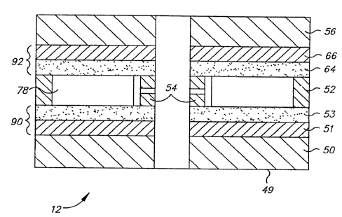
Fig. 5 is a cross-sectional view of the optical data storage disk 12
with multiple phase-change WORM active recording layers 51
and 66. Disk
12 has a substrate 50 having an outer face 49 onto which the
laser beam is
incident. Substrate 50 is preferably made of polycarbonate,
amorphous
polyolefin (APO), polymethylmethacrylate (PMMA), or glass and
is
non-absorbing at the recording wavelength. Substrate 50 is
preferred to
have a thickness of 1.2 mm but other thicknesses can be used.
Pre-addresses and pre-grooves for the tracking servo of the
laser light
beam may be formed on the surface of substrate 50 opposite
outer face 49.
A recordable thin film 51 of active phase-change WORM material
is
deposited by sputtering or evaporation on substrate 50. The
preferred
material is a phase-change type alloy of AXSn~,Sbz (3~<x<45~;
1~<y<40~,
45~<z<96~; and x+y+z=1000 of thickness 2 to 15 nm, where A
can be In, Cr,
Bi, Si, and other transition metals. This type of phase-change
alloy is
described in U.S. Patent 4,960,680. However, as described in
that
patent, the material is a single layer with a thickness of
at least
approximately 20 nm. If this material is thicker than 20 nm,
its light
transmissivity is less than 15~. Thus the material at the conventional
thickness is not suitable for multiple recording layer optical
disks which
requires transmissivity greater than approximately 35~, which
can only be
achieved for thicknesses less than approximately 7.5 nm. Further,
a mere
reduction of thickness to less than 7.5 nm to increase light
CA 02220879 1997-11-12
WO 97/02564 PCT/GB96/00527
8
transmissivity causes other problems. For thicknesses less than
approximately 7.5 nm, the reflectivity of the amorphous and crystalline
phase is too low to assure accurate focusing and tracking, or reading of ,
data with a low error rate. Also, such a thin phase-change layer is
susceptible to corrosion if not protected.
In the present invention, one or more additional films, such as
optical interference film 53, is deposited in contact with recording
layer 51. By use of the optical interference effects of thin films, the
transmissivity, reflectivity, and absorptivity of the multi-thin film
recording stack 90 (active recording layer 51 and film 53) can be adjusted
by varying the individual layer thicknesses. Film 53 and recording layer
51 together form an interference structure. Constructive interference
occurs if the thickness of film 53 is properly selected, based on its
thickness and the real part (n) of its index of refraction. A large
difference in the value of n for film 53 relative to the indices of
refraction of its adjacent layers (recording layer 51 and air) increases
the interference effect for a given film thickness and will optimize the
signal contrast and the reflectivity of the recording stack 90. Optical
interference film 53 should also have low absorption (low imaginary part
of its index of refraction, i.e., low extinction factor k) so that when
the light spot is focused on second recording layer 66 it will transmit
through recording layer 51 and film 53 with minimal absorption.
Dielectrics such as SiOx, TiOX, ZrOX, CuXO, SiN, SiC, amorphous Si, or
organic polymers and the like are preferred for optical interference film
53, and can be deposited by sputtering, evaporation or spin coating on
active recording layer 51. Other suitable materials for optical
interference film 53 are oxides and nitrides of an element selected from
the group consisting of A1, Ti, Zr, Cu, Hf, Ta, Nb, Cr and W. Dielectrics
sych as zn and Cr mixed with one or more of S, Se and Te are also usable.
These materials may be in the amorphous or crystalline phase. If in the
amorphous phase, a wide range of compositions are allowable. For example,
SiOx may have a composition with 1<x<2.1. The optical interference
effects are calculated using standard thin film interference calculations
as described, for example, in Optical Properties of Thin Solid Films, O.H.
Heavens, Academic Press, 1955.
Another important characteristic of film 53 is low thermal
conductivity. with an active recording layer 51 that has high
transmissivity (i.e., low absorption), the write sensitivity of the
phase-change material will not be as high as in a conventional thick ,
highly absorbing phase-change layer. Therefore, with film 53 in contact
with active recording layer 51, the thermal conductivity of film 53 should
be small so as to reduce heat flow from the active recording layer 51
while the laser is at the write power level. In general, a non-absorbing
CA 02220879 1997-11-12
WO 97/02564 PCT/GB96/00527
9
material with a thermal conductivity less than 0.1 w/cm-K can be used for
film 53. For example, SiOx has a thermal conductivity of 0.015 w/cm-K
at 400 degK. The requirement of low thermal conductivity for film 53 can
be relaxed if higher laser power is available. Dielectric film 53 also
!i acts as a protective coating for thin active recording layer 51, which is
especially desirable if the spacer between recording layers is an air gap.
A spacer layer 78 in the form of an air gap is adjacent to the
optical interference film 53 and separates the two recording layers 51,
66. A layer 64 of a non-absorbing protective layer, such as a spin coated
photo-polymer (W-curable acrylate) may deposited on the second active
phase-change recording layer 66. Because recording layer 66 can be thick,
layer~64 may not be required either as a protective layer or to enhance
the performance of recording layer 66. The second recording layer 66 is
1°_~ the last active recording layer in the multiple recording layer
optical
disk and does not have to be transmissive. Thus it can be of conventional
thickness, e.g., 20-200 nm. with a thicker active recording layer 66 the
absorptivity is higher, as compared to active recording layer 51.
Therefore, the write sensitivity for layer 66 can be higher so the thermal
conductivity of non-absorbing protective layer 64 is not as critical as
for film 53. Thus, layer 64 can be selected from low absorption
dielectrics such as those described above for layer 53 with a thickness
from 10 nm to several microns. The stack 92 of second recording layer 66
and protective layer 64 are deposited on the second substrate 56.
Substrate 56 can be formed of the same materials as substrate 50 or of
opaque materials such as opaque plastic materials and metallic materials,
such as aluminum.
In a preferred embodiment of optical disk 12, as shown in Fig. 5,
with a laser operating at a 780 nm wavelength, substrates 50 and 56 are
polycarbonate of 1.2 mm thickness. First active recording layer 51 is
InlSSnzoSb65 of 9 nm thickness. This film by itself transmits approximately
29~ of the incident light and has a reflectivity of 13~. By depositing
150 nm of an optical interference film 53 of SiOz with n = 1.5, the
transmissivity of the stack 90 becomes 41~ and the reflectivity is 20~.
Such a phase-change wORM recording structure with a transmissivity greater
than 35~ and a reflectivity greater than 10~ is required for reliable
operation with good signal to noise with existing laser diode sources.
The air-gap 78 is 200 microns thick. The second active recording layer 66
on substrate 56 is InlSSnzoSbss of 75 nm thickness. Protective layer 64 is
a spin coated photo-polymer (W-curable acrylate) of 2 microns thickness.
If the laser light is of a shorter wavelength to reduce the spot size and
thereby increase the recording density, adjustment of the thickness of
recording layer 51 and film 53 is needed. For example, for laser light at
CA 02220879 1997-11-12
WO 97/02564 PCT/GB96/00527
a 500 nm wavelength, the thickness of film 53 is optimally 110 nm, with
recording layer 51 having a thickness of 8 nm.
In a particular example of a two-layer disk similar to the
5 above-described preferred embodiment according to the structure of Fig. 5,
the active recording layers 51, 66 were formed of InlSSnzoSb65 with the '
transparent dielectric layers 53, 64 formed of Si02 . Layer 51 was 8 nm
thick and sputter deposited on polycarbonate substrate 50. The dielectric
layer 53 was sputter deposited to a thickness of 15 nm on layer 51. The
10 second data layer 66 was 75 nm thick and sputter deposited on
polycarbonate substrate 56. .Protective layer 64 was 15 nm of SiOz sputter
deposited on active layer 66. The two substrates were then bonded
together to have an air-gap 78 with a thickness of 300 microns. The two
recording stacks 90, 92 (recording layers 51, 66 and their associated
optical interference layers 53, 64) had values of transmissivity,
reflectivity and absorption as shown in Table 1 below:
Tsble 1
Layer NumberThiclmoss TranamissivityRoflactivityAbsorption
(soy FiQ. (nm> (%> (%>
s)
1 (51) 8 44 17 39
(L~y~t 53 15
)
2 (66) 75 1 31 68
(Lnystt 15
64)
This two layer disk was tested on a dynamic test stand. A laser
beam of 780 nm wavelength was focused through a 0.55 numerical aperture
lens. The disk was rotated so that the local media velocity was 10.7 m/s.
Laser pulses of 12 ns were used to record pulse width modulation (PWM)
data of 8 clock cycles length. Each clock cycle (T~) was 35.4 ns.
Figs. 6A and 6B are graphs of readback data of mark trailing edge to
trailing edge (TE-TE) °jitter" for each of the two recording layers as
a
function of laser write power. Jitter is a measure of the deviation of
the written mark transitions from their ideal locations on the disk. Low
fitter at the correct mark length is important to ensure that data is read
back with minimal errors. It is desirable to have the worst case fitter
be less than five percent of T~, which would be 1.8 ns in this case of a
35.4 ns clock. As shown in Figs. 6A-6B, the readback data on both
recording layers, at the correct mark length of 8TH=283.2 ns, exhibited
low fitter of less than 1.2 ns. The write power needed to achieve this '
low fitter is less than 23 mW for both recording layers, which is
achievable with presently available commercial lasers.
CA 02220879 1997-11-12
WO 97/02564 PCT/GB96/00527
11
The preferred embodiment of the present invention has been described
for an air-gap structure as shown in Fig. 2A, but is fully applicable
with the other disk structures as shown in Figs. 2B-2D.
Fig. 7 is a cross-sectional view of another embodiment of the
optical disk 12, designated 12'. Elements of disk 12' that are
similar to
' elements of disk 12 are designated by a prime number. The first
recording
layer 51' has two light-transmissive films 55, 57 deposited
on it in place
of film 53 (Fig. 5). In certain cases where the choice of a
high index of
refraction and low thermal conductivity material is not available,
for
example due to difficult manufacturing requirements, double
transparent
thin films can then be used. Thus in disk 12' the function of
single film
53 is accomplished by the combination of films 55, 57. Film
55 should
have low thermal conductivity but not necessarily high n, whereas
film 57
should have high n but not necessarily low thermal conductivity.
Dielectrics such as SiOX, TiOx, ZrOx, CuXO, or organic polymers
and the
like are preferred for film 55. Low absorption dielectrics such
as those
described above for layer 53 (Fig. 5) are preferred for film
57. The
optical properties of recording layer 51' can be optimized by
adjusting
the thicknesses of layers 55 and 57. For example, Si02 with
a thickness
of 10-80 nm can be used for film 55 and SiNx with a thickness
of 20-100 nm
can be used for layer 57. Another change can also be made for
second
recording layer 66'. The thickness of protective layer 64' can
be
adjusted, making use of the optical interference effect, to
maximize the
signal contrast for the second recording layer 66'. SiOX may
be deposited
by evaporation or sputtering on active recording layer 66' to
a thickness
range of 50-200 nm. With this thin SiOX layer 64', the signal
contrast
increases by a factor of 1.3 to 2.2 as compared to an active
recording
layer 66' without any optical interference coating. This increase
in
contrast is useful where improved signal to noise is required
as, for
example, in the case of high-density, pulse-width-modulation
(PWM)
recording. Furthermore, the dielectric coatings 55 and 57 on
recording
layer 51' can be deposited on substrate 50' between the substrate
and
active recording layer 51' instead of on top of active recording
layer
51'. This is because the placement of dielectric coatings between
recording layer 51' and substrate 50' is sometimes desirable
due to
manufacturing issues such as adhesion of various layers.
Fig. 8 is a cross-sectional view of another embodiment of the
' optical disk 12, designated 12. Elements of disk 12~ that are
similar
to elements of disk 12 are designated by a double prime number.
In a
manner similar to optical disk 12' in Fig. 7, multiple recording
layer
WORM disk 12 has two non-absorbing films 72 and 74 near active
recording
layer 51. The difference is that the active recording layer
51~~ is
sandwiched between non-absorbing films 72, 74. Dielectric film
72 is
deposited directly on substrate 50", the active phase-change
recording
CA 02220879 1997-11-12
WO 97/02564 PCT/GB96/00527
12
layer 51" is then deposited on film 72, and film 74 is then deposited on
active recording layer 51". The laser light passes through the
non-absorbing film 72 before it reaches the recording layer 51". This
trilayer thin-film recording stack 90" also takes advantage of the
optical interference effects to maximize performance. The function of
films 72, 74 is identical to film 53 of disk 12 in Fig. 5. Thus, '
films 72, 74 should have low thermal conductivity and high n. The
advantage of this structure over the structure of disk 12 is that under
some high write power conditions, ablation of the recording layer may take
place. Ablation in a phase-change medium is not desirable because it may
increase error in the placement of data marks. with a sandwich structure
as shown, the possibility of ablation in the recording layer is minimized.
In a preferred embodiment of the structure of Fig. 8, with a laser
operating at a wavelength of 780 nm, substrate 50" and 56" are
polycarbonate of 1.2 mm thickness. First dielectric layer 72 is SiOz of
2 nm thickness. First active recording layer 51" is In,,5Sn2oSb65 of 8 nm
thickness. The second dielectric layer 74 is spin-coated W-curable
acrylate of 2 microns thickness. The air-gap 78" is 200 microns thick.
The second active recording layer 66" on substrate 56" is InlSSnZOSb65 of
75 nm thickness. Protective layer 64" is a spin-coated W-curable
acrylate of 2 microns thickness.
The present invention has been described and shown in the drawings
for a multiple recording layer disk with only two recording layers.
However, it is possible to have more than two recording layers. One or
more additional recording layers and associated optical interference films
can be located between the first and second recording layers. For
example, if a third recording layer (and a second optical interference
film in contact with it) is included in the preferred embodiment of
Fig. 5, the first recording layer would be InlSSnZoSb65 with a thickness of
7 nm and the first optical interference film would be SiOz with a
thickness of 150 nm. The third recording layer would be InlSSnZOSb65 with a
thickness of 7 nm and the second optical interference film would be Si02
with a thickness of 150 nm. This would result in a transmissivity of 50~
for each recording stack so that 25~ of the laser light incident on the
first substrate would reach the second or farthest recording layer.
In place of a phase-change type alloy of AxSnySbZ, other material
compositions that undergo an amorphous to crystalline transformation and
have a reflectivity difference associated with those two structurally
distinct states may be used for the phase-change WORM recording layers ,
(51, 51~, 51°, 66, 66', 66").. A general principle guiding the choice
of
applicable compositions is that the materials be at or close to a
stoichiometric composition. This is a composition at which little or no
phase separation occurs during crystallization. This condition may be
CA 02220879 1997-11-12
WO 97/02564 PCT/GB96/00527
13
obtained for materials which crystallize into stable phases or metastable
phases. Generally, those materials which crystallize the quickest are
- most applicable. Additionally, for materials that do not crystallize
extremely fast, the thin film structure should be relatively insulating to
reduce the cooling rate. This is to prevent the crystallized spot from
converting back to the amorphous phase due to melting of the recording
layer by the focused laser beam. This last requirement is to ensure that
the material can only be written once. This means that there should not
be a high thermal conductivity material, such as a metal layer, either in
direct contact with the recording layer or separated from it by a thin
(e. g., less than approximatley 30 nm) dielectric layer.
Among the materials which are most suitable binary compositions are
GeTe, SnTe, PbTe, SbSe, Sb2Se3, Sb,l_X,Se with 0<x<p.4, BizSe, Sbi2Se3, Bi2Te,
Bile, Bi2Te3, Sb2Te, SbTe, Sb2Te3, TeSi, Ag2Se, AgSe2, Ag2Te, Ag3Te2, AgTez,
Au2Se" AuTe2, GaSb, and GeSe. Additionally, these compositions can be
slightly off stoichiometry and crystallize extremely quickly by adding
nucleating agents such as Ti, Pd or Cr. Ternary compositions suitable for
phase-change wORM include compositions along the composition tie-line
connecting GeTe with SbZTe3 and in particular, GeSb2Te4, Ge2SbzTeS, GeSbqTe,
or compositions along that tie line with small amounts of excess Sb, Ti,
Pd, Sn or Cr. Other materials include In3SbTe2. Another material
composition is (InSb)1_x(GaSb)x where .5<x<=1. Also active recording films
such as sub-oxide films of the type TeOx, GeOx. SbOx, and InoX with
metallic additives (e. g., Pd, Ni, Cu) are also applicable. These suboxide
systems also make use of the thermally-driven amorphous-to-crystalline
phase transition as the recording mechanism. For each of these materials,
new thicknesses for the non-absorbing layers 53, 55, 57, 64, 72, and 74
(and their primed counterparts) are determined based on the teaching
described above.
The invention has been described in the embodiment of an optical
disk drive. However, there are other types of optical data storage
systems to which the invention is applicable. These systems usually have
the feature that the medium upon which the data is stored can be removed.
The common systems are those using optical media in the form of a tape or
card. The drive associated with the tape or card moves the tape or card
by translation, instead of rotation in the case of a disk, for the reading
and writing of data. It is desirable to also increase the data storage
capacity of optical tape and cards by use of multiple recording layers of
phase-change WORM material. In the optical tape or card the multiple
recording stacks may be supported on an opaque substrate and covered with
a transparent protective layer onto which the laser light is incident. In
this case the protective layer functions like the previously described
disk substrate. Both the tape or card protective layer and the disk
CA 02220879 1997-11-12
WO 97/02564 PCT/GB96/00527
14
substrate are transparent members that have an outer surface onto which
the laser light is incident and through which the laser light travels to
the recording stacks.
a