Note: Descriptions are shown in the official language in which they were submitted.
CA 02226495 1998-O1-07
WO 97/05742 PCT/GB96/01805
-1-
THERMAL SENSING SYSTEM HAVING A FAST RESPONSE CALIBRATION DEVICE
' This invention relates to a thermal sensing system and more particularly to
both
imaging and non-imaging sensing systems incorporating an array of photon-
detecting
~ elements.
Thermal imaging systems are known in the prior art. Such imaging systems can
involve either series or parallel processing. In the former case a scene is
scanned and
each component of the scene is focused sequentially onto a detector. These
systems
are not easy to design however if compactness is important, the scanning
mechanism
renders the adaptation to lightweight imagers extremely difficult. An
alternative
arrangement for area imaging is to employ many detectors to sample
simultaneously
distinct sections of the scene. A major disadvantage of this system is that
the transfer
function from incident infrared flux to output signal (detector signal) is
particularly
sensitive to variation between detecting elements. This results in an image
degraded
by fixed pattern noise arising from sources both within and independent of the
detecting elements. Imperfections in the optical system (e.g. vignetting) and
variations
in the associated electronic circuits are examples of the latter case.
Photodetector
sources can be static variations in characteristics (e.~;. area. quantum
efficiency or cut-
'?0 off wavelength) or dynamic instabilities (temperature. offset voltage and
slope
resistance all drift over a period of time) which give rise to the need for
regular array
recalibration. Additionally Ilf noise introduces an error which increases with
the
period between calibrations. Compensation for inter-detector variations is
particularly
important in "staring" applications which measure the absolute radiation
intensity
within a scene. Scanning imagers measure only changes in intensity across a
scene.
The output from a staring array is thus of poor contrast in comparison.
Non-imaging thermal detectors are also known in the prior art. They have
applications
in areas such as robotics and missile guidance systems for which human
interpretation
of detector output is not required. The actual detecting elements are similar
to those
described above in relation to imaging systems. In non-imaging systems however
an
'SUBSTITUTE SHEET (RULE 26)
CA 02226495 1998-O1-07
WO 97/05742 PCT/GB96/01805
object (robot or missile) is arranged to respond to a particular signal
appearing on the
detectors. This recognition feature may vary in its complexity. For example,
pattern
recognition can be linked to a number of response options or a less complex
reflex can
result in steering towards the achievement of a characteristic detector
response.
Staring arrays are particularly suitable in satisfying the lightweight
requirements of
missile systems. However in such missiles the detector system is subject to
rapid
temperature change as the missile cone heats up during flight. Frequent
recalibration
is necessary in order to maintain an acceptable accuracy.
An imaging system incorporating a detector array is disclosed by P.N.J.Dennis
et al. in
Proc. SPIE 572 2? (1985). The authors describe a two dimensional close packed
array
of cadmium mercury telluride detectors interfaced to a silicon charge coupled
device
(CCD). Infrared light incident on a detector elicits a response signal which
is injected
into the CCD and integrated over a period of time (the stare time). The
subsequent
signal processing system addresses the fundamental problems of poor contrast
from
the infrared scene and nonuniformity of detector element responses. The
nonuniformity correction is made by exposing the array to two uniform scenes
of
different temperature with an arrangement of mirrors used to introduce them
into the
optical path. From measurements of stimulus infrared flux and detector
response a
?0 correction factor is derived for each individual detector by forcing a
uniform scene to
give rise to a uniform image. 'The signal response is fitted linearly to
incident radiation
intensity and an offset and gradient derived to describe the transfer function
for each
detector in the array. All values of signal response at all detectors can thus
be
converted into corrected incident flux values. Array calibration in this way
is
performed periodically (perhaps hourly or daily) and the updated correction
factors
applied to subsequent measurements. This compensates for 1/f noise and
detector
parameters drifting over a period of time as a result of, for example,
temperature
changes.
A disadvantage of such sensing systems is that possible reference temperature
sources
limit the performance in terms of speed and compactness. If physically
separate
SUBSTITUTE SHEET (RULE 26)
CA 02226495 1998-O1-07
WO 97/05742 PCT/GB96/01805
reference scenes are used then the sensor requires an optical system with
considerable
complexity and bulk. Alternatively reference temperatures could be supplied by
a
' Peltier cooled/heated reference plane but the finite time taken to adjust to
temperature
l
leads to a lengthy calibration process.
A combination of both these techniques is disclosed in US Patent 4 419 692.
This
patent is concerned with a mufti-detector scanning thermal imager which
already
possesses a bulky scanning mechanism and so no particular advantage is gained
by
physical reduction of the reference system. Scanning thermal imagers are
frequently
used with an array of detector elements in order to increase sensitivity.
Uniformity
corrections then have to be incorporated into the signal processing. In this
device
errors are reduced over the thermal range present in the scene under
observation by
allowing one of three thermo-electric references to be varied by the operator
to provide
a reference level at the midpoint of the scene thermal range. The Peltier
cooler used to
provide this third reference is varied between scenes in order to adapt the
calibration
technique to the characteristics of each particular scene. Three reference
temperatures
are used as opposed to two in the Dennis system above: one provides a do level
about
which the ac temperature variations detected by the scanning imager are
referenced
and the remaining two provide the uniformity correction for the detector
array.
?0
Another correction mechanism. main used with a scannin~~ thermal imager. is
described in UK patent ? 2?~ 914 A. A single reference source is used which
removes
the requirement for additional optical components to bring different sources
into the
optical path. A disc coated to provide regions of differing reflectivity is
rotated
between this single reference source and the thermal imager. The differing
reflectivities permit different proportions of the radiation emitted from the
source to be
passed to the imager. Thus different effective temperatures can be used as
references.
The mechanical spinning of the disc is synchronised with the scanning
mechanism to
arrange for the reference temperatures to be passed to the thermal imager only
during
inactive periods of the scan. However this technique still requires mechanical
movement mechanisms for both the disc spinning and scene scanning. Overall,
this
SUBSTITUTE SHEET (RULE 26)
CA 02226495 1998-O1-07
..
:_
.. . ~. , ..
s v . v c :
...
imager is still bulky and unsuitable for some applications. Furthermore there
is a Iimit
to the number of differing-reflectivity sections which can be incorporated on
the disc.
Each level of flux must be viewed for sufficient time to allow the imager to
adjust to
the new reading and the majority of the disc must be uncoated to correspond to
the
time needed to view the scene.
It is an object of the invention to provide an alternative form of thermal
sensing
system.
The present invention provides a thermal sensing system including an array of
photon-
detecting elements and switching means for interchanging between scene
observation
and detector calibration modes of the system characterised in that the system
also
includes a variable luminescence device arranged to provide array illumination
for
calibration purposes, the variable luminescence device having flux emission
which is
variable to within 10% of a steady state value .in a settling time of less
than ten
seconds.
The invention provides the advantage that it can be constructed in compact
form and is
capable of providing a means for fast, frequent and accurate correction for
nonuniformity of detector elements.
The variable luminescence device is preferably electrically controllable and
capable of
readjusting the intensity of flux emission to within 1 % of a steady state
value in a
settling time of less than one second. Operation within the specified limits
may be
provided for if the variable luminescence device is a semiconducting device
which in a
preferred embodiment is an infrared light emitting diode (IR LED) which is
electrically biasable to provide both- positive and negative infrared
luminescence
emission. P.Berdahl et al. in Infrared Phys. ~(2-4) 667 (1989) explain
positive
luminescence as an increase in the radiation emitted from a body when its
situation of
thermal equilibrium is perturbed by some exciting mechanism. Similarly
negative
luminescence is a decrease in emitted radiation relative to equilibrium
thermal
emission. The IR LED ideally has a predetermined relationship between emission
AMENDED SHEET
IPEA/EP
CA 02226495 1998-O1-07
WO 97/05742 PCT/GB96/01805
~5_
intensity and biasing strength. This provides capability for rapid
calibration. In this
embodiment the system lends itself to providing a more accurate uniformity
correction
than is possible on a similar timescale in prior art thermal sensors. One
disadvantage
of prior art thermal sensors is that detector nonuniformity is not linear over
the
temperature range of interest and making a nonlinear correction requires at
least three
reference scenes to emit radiation onto the detector. The fast settling speed
of IR
LEDs provides for a series of different intensity reference fluxes to be used
in the
uniformity correction and so the calibration function relating individual
detector signal
response to incident flux can be fitted to a polynomial expansion which does
not
assume linearity.
Furthermore. an IR LED with these characteristics is capable of providing a
reference
temperature which is optionally above or below ambient temperature. It can
cover a
greater temperature range than the commonly used Pettier cooler. Practically,
a Pettier
cooler is run in reverse to reach temperatures above ambient and the range
covered is
only a few tens of degrees. An IR LED is capable of simulating temperatures
across a
range far in excess of that of the Pettier cooler/heater.
These advantages are apparent in both scanning and staring thermal sensors
which use
?0 an array of detector elements and this invention should not be seen as
restricted to
either. However. the advantages are more significant when the IR LED is used
to
provide the uniformity correction for a staring array. A staring thermal
sensor already
admits of compact construction and greater accuracy is important to enhance
the low
contrast generally achievable. Improving contrast without significantly
increasing the
size is an advance which extends the utility of both staring thermal imagers
and similar
non-imaging sensors.
r
The switching means is preferably arranged for the detector array to receive
radiation
from the variable luminescence device between intervals of scene observation.
In one
embodiment the switching means is switchable between a first configuration in
which
radiation from a scene under observation is incident'on the detector and a
second
SUBSTITUTE SHEET (RULE 26)
CA 02226495 1998-O1-07
WO 97/05742 PCT/GB96/01805
_6~
configuration in which radiation from a variable luminescence device is
incident on
the detector. This provides the advantage that the time for which the detector
array is
idle is reduced to the time taken to switch between these two configurations
only.
Prior art imagers with n physically separate reference scenes require a
switching means
which provides for n + 1 different configurations.
The thermal sensing system of the invention may include a computer arranged to
derive a corrective function for each detector in the array from the detector
output
response to the variable luminescence device and in accordance therewith to
correct
I 0 the detector output response to an observed scene. This provides the
advantage of fast
calculation which allows the thermal sensing system of the invention to
incorporate
any practical detector array. More specifically the computer may be arranged
to
calculate the relationship between the intensity of~ infrared radiation (F,)
incident on a
detector of the array and magnitude of electrical signal response (s",)
therefrom when
the source of the radiation is the variable luminescence device arranged to
provide
infrared flux at a predetermined intensity. The computer is then also arranged
to apply
the derived relationship as a correction to signals output from that detector
in the
course of scene observation. The variable luminescence device may be arranged
to
emit radiation with at least three different predetermined intensities for
array
?0 calibration purposes. and the computer is then arranged to calibrate each
detector in
the array by fitting the predetermined radiation intensities to detector
signal responses
as a power series expansion of at least quadratic order. In this way the
advantage of
accurate (nonlinear) correction factors over a range of incident flux
intensities
described previously can be combined with the advantage of fast calculation
also
described above.
The computer is preferably arranged to use the derived relationships between
incident
flux and detector response and thereby to apply a uniformity correction to the
array
signal responses. In imaging systems the computer is also arranged to pass the
corrected signals to a means for display arranged to indicate strength of
signal from
SUBSTITUTE SHEET (RULE 26)
CA 02226495 1998-O1-07
WO 97/05742 PCT/GB96/01805
each individual detector at a position in the image corresponding to that in
the detector
array.
The computer is also preferably arranged to update the derived relationship
between
incident flux and each single detector signal response at intervals and to
apply the
updated relationships to subsequent observations. This provides the advantage
of
reduction in the effect of detector drift over a period of time. In this
embodiment the
computer may be arranged to update the derived relationship between incident
flux
and each single detector response more frequently than once per hour. The
drift
associated with the Ilf noise alone can half the sensitivity of a high
performance 2D
detector array in less than one hour. The updating frequency may be adaptive
to the
observed scene. It can be chosen as appropriate in that detector properties
change with
scene temperature rendering a previous uniformity correction inaccurate.
Resolution
will therefore be lost in proportion with the rate of mean temperature change
within
the scene and frequent updating will be necessary in order to resolve small
temperature
differences. In prior art imagers the settling time required by Pettier
coolers prohibits
such frequent checks and severe distortions can result with a high temperature
scene.
In a non-imaging.: missile homing system the errors introduced by the rapid
variation in
ambient temperature as the missile is launched can be countered by frequent
'_'0 recalibration of the detector array in accordance with this invention.
Prior art homine
systems provide for frequent recalibration by a rapid switching between
separate cold
and hot reference scenes. Such a switching mechanism however is costly in
terms of
minimising system size. A single-source IR LED facilitates frequent
recalibration
without the need for such a switching mechanism.
The IR LED may be arranged to emit reference fluxes which cover a similar
intensity
' range to that of the radiation emanating from a scene under observation.
This provides
for the uniformity correction to be derived from reference radiation
characteristic of an
observed scene. This enables error correction to be most effective in the
region of the
temperatures actually being measured. The dynamic range of the IR LED makes an
SUBSTITUTE SHEET (RULE 26)
CA 02226495 1998-O1-07
WO 97/05742 PCT/GB96/01805
~g~
imager incorporating such a reference source capable of effective imaging of a
wide
variety of environments.
r
In a further embodiment the computer may be arranged to control the current
through
6
the IR LED in response to detector output signals. The current may be
controlled in
the first instance in response to uncorrected signals and subsequently to
corrected
values of incident flux intensity. This provides the advantage that
calibration fluxes
are automatically controlled to be characteristic of an observed scene. Prior
art sensors
do not have this flexibility and reference temperature scenes may not bear any
relation
to a scene under observation and the calibration is therefore inaccurate. This
advantage is particularly relevant when small differences from background are
important.
In particular. the variable luminescence device may be a light emitting diode
of
cadmium mercury telluride or an indium antimonide based material such as
InAISb,
InGaSb.
In a further aspect the present invention provides a method of applying a
uniformity
correction to a thermal sensing system including an array of photon-detecting
30 dements. the method comprising the steps of:-
(a) irradiating the detector array with infrared radiation from a variable
luminescence device whose luminescence is adjustable to within 10% of a
selected value with an adjustment time of less than ten seconds, the variable
luminescence device also having predetermined flux output characteristics,
(b) deriving correction factors for each detector in the array from the output
responses to predetermined fluxes, and
(c) applying the correction factors to output signals from the array detectors
arising
when infrared radiation from an observed scene is incident on the detector
array.
SUBSTITUTE SHEET (RULE 26)
CA 02226495 1998-O1-07
WO 97/05742 PCT/GB96/01805
..
The invention provides the advantage that a uniformity correction can be
calculated
and applied with an accuracy and speed appropriate to the requirements of the
situation
in which the thermal sensing system operates.
Steps (a) and (b) may be repeated at intervals in order to update the
correction factors
derived in Step (b) and thus there is the additional advantage that the
uniformity
correction can be updated with a frequency appropriate to the system's
operating
requirements.
Array irradiation in Step (a) may be performed with at least three different
predetermined flux intensities output from the variable luminescence device
and the
correction factors of Step (b) derived by fitting the incident radiation
intensities to a
power series expansion to at least quadratic terms of detector signal
response. This
provides the advantage of dealing with nonlinearity in the detector response
to incident
flux across the range of radiation intensities which may emanate from the
observation
scene.
In order that the invention might be more fully understood. embodiments
thereof will
'?0 now be described with reference to the accompanyin~~ drawing in which:
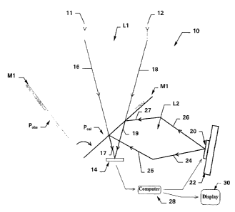
Figure ! illustrates schematically a proposed mode of operation for performing
a
uniformity correction using a negative/positive luminescent device.
With reference to Figure 1. there is shown a thermal sensing system in an
imaging
implementation indicated generally by 10. The system 10 incorporates an
objective
lens LI which focuses infrared (IR) radiation, indicated by rays Il, 12,
emanating
from an observed scene (not shown) onto a two-dimensional array of
microdetectors
1-1. A two-position mirror MI is in either an observation position Pubs
(indicated by a
dashed line) or a calibration position P~Q~ (bold line). When the mirror MI is
in
position Pubs then the path of the radiation focused by the lens LI
corresponds to the
SUBSTITUTE SHEET (RULE 26)
CA 02226495 1998-O1-07
WO 97/05742 PCT/GB96/01805
-10-
region between the rays 16. 17 and 18, 19. An indium antimonide light emitting
diode
(LED) 20 is mounted on a Peltier cooler/heater device 22. A lens L2 passes IR
radiation emitted by the LED 20 to the detector array I -~ via reflection from
the mirror
MI in its position Pal. The path followed by this radiation beam is contained
within
the rays 2-~. 25, 17 and 26. 27, 19. A computer 28 processes information
received
from the detector array I-~, passes information to a display apparatus 30 and
controls
current input to the LED 20.
When exposed to an IR flux the detector array 1-~ responds with a
corresponding array
of electronic signals s", 1 <_ n <_ N, where s" is the signal from the nth
detector in the
array and l'~' is the total number of detectors in the array.
In a situation of radiative equilibrium the IR LED 20 will be emitting as much
radiation into its surroundings as it absorbs from them. However this
equilibrium
situation is disturbed by the application of an electric current. In such a
situation the
IR LED 20 will either be a net emitter (positively luminescent) or a net
absorber
(negatively luminescent) of IR radiation. The mode of operation depends on
whether
the LED is forward or reverse biased. The intensity of- IR radiation emitted
(or
absorbed) is dependent on the strength of current flowing. The IR LED ?0 is
?U calibrated so that for any particular value of current tlow~ing and any
sense of biasing
the intensiy of IR radiation emitted or absorbed by the IR LED is known. The
Peltier
device ? 2 serves to hold the temperature of the IR LED stable at the
temperature at
which its IR emission was calibrated. In this way the IR LED 20 acts as a
calibrated
variable-intensity source or sink for IR radiation. This IR flux can
equivalently be
regarded as that emanating from, or absorbed by, a body at a particular
(nonequilibrium) temperature T. It is not strictly necessary to use a Peltier
device 22
to stabilise the temperature of the IR LED. All that is required is that the
IR flux is
maintained at a level appropriate to the temperature simulation required. In
an
alternative embodiment this is done by implementing an electronic feedback
mechanism which adjusts the current through the IR LED in response to a direct
measurement of the LED temperature.
SUBSTITUTE SHEET (RULE 26)
CA 02226495 1998-O1-07
WO 97/05742 PCT/GB96/01805
~11--
The detector array 1=~ receives radiation from the IR LED 20 when the mirror
MI is in
position Pal. With this arrangement a known IR flux emitted by the LED 20 is
passed
by the lens L2 and reflected by the mirror Ml at P~u, to the detector array 1-
~. The
known flux emitted from the IR LED 20, say F~, is assumed to then be incident
on
each detector of the array I-/. To correct for nonuniformity across the array
the signal,
s,", from the nth detector is interpreted as the response to F,. The
relationship between
incident flux and signal response from the nth detector is fitted to a
polynomial:
F, = a,l + b.~'~~r + ~ya~ + d"s~"3 + ........ (I)
where the constants a", b". c". c~", etc. are specific to the nth detector of
the array only.
The current through the IR LED 20 is adjusted to a variety of strengths in
forward and
reverse biasing directions. This provides for further reference fluxes, F,,
F3, F.~, etc. to
be directed onto the detector array. 'The time in which the IR LED stabilises
at a new
flux value is less than a second, a response which compares very favourably
with
alternative methods of variable flux provision e.g. a cooled/heated reference
plane for
which temperature control (equivalently. flux control) is provided by a
Peltier
?0 cooleriheater. If the total number of reference observations is given
hs° i",ur then a set
oh simultaneous equations in the form of Eyuatioja lI) can be derived for the
nth
detector:
Fi = ~n + bn5~in 1 Crrsin' + drrs-in3 + ....... , I = I, 2,3,......l~n~ (2)
The accuracy with which the relationship between IR flux F and signal s can be
deduced for each detector depends on the number of reference observations made
i.e.
the polynomial can only be solved as far as the (i",~ - 1 )th power of s.
Similar sets of simultaneous equations are derived and solved for each of the
N
detectors in the array with the aid of a computer. The analogue detector
signals are
SUBSTITUTE SHEET (RULE 26)
CA 02226495 1998-O1-07
WO 97/05742 PCT/GB96/01805
~12~
first converted into a digital representation and a computer is used to set up
and solve
the N series of i",~ equations. The N sets of values an, bn, c", d", etc. are
then stored in
the computer memory for later use in applying the uniformity correction.
During normal operation of the thermal imaging system 10 in observing a scene,
the
minor MI is pivoted to position PobS. Radiation from the scene is then focused
onto
the detector array I=~ and the output electronic signal from each detector in
the array is
recorded. This yields N signals which are then converted into N uniformity-
corrected
IR flux values using the a", b", c", d", etc. coefficients from Equation (2)
to perform
the calculation shown in Equation (3)
obs obs obs 2 obs 3
F" - an + b,~" + c"(sn ) + d"(s" ) + ........ ~3)
where the superscript obs indicates that the signals are measured while the
system is in
observation mode and the flux derived is hence the IR flux incident on the nth
detector.
To reconstruct the thermal image the IR radiation intensity incident on the
nth detector
at array position D" is displayed visually on a display screen at pixel
position P".
?0 There is a direct geometric correspondence between the array position D"
and screen
position P" and so features appearing at a particular position in the scene
under
observation are displayed at the corresponding position in the thermal image.
The lV
values of FN bs are thus used to construct a thermal image with reduced fixed
pattern
noise.
The relationship between the signal response of a detector and the incident
flux
necessary to produce that response can be graphically represented by a curve
covering
the range of detector operation. The method of obtaining the constants a, b_
c, d, ....
outlined above amounts to fixing a few discrete points on this curve
(reference fluxes)
and fitting these points to a polynomial function in order to interpolate for
intermediate
values. Thus an approximation to the true curve is derived and used to
calculate
SUBSTITUTE SfiEET (RULE 26)
CA 02226495 1998-O1-07
WO 97/05742 PCT/GB96/01805
-13-
incident flux (F'"°bs) from a measured detector signal response
(s"°bs). Clearly the
greater the number of discrete points that are actually measured on this curve
then the
' more accurate are the points derived by interpolation. However these
reference
measurements are made while the thermal imaging system 10 is in its
calibration mode
and in this state it cannot be making any measurements in its observation
mode. Thus
a balance must be found between the desire for accuracy in the calibration
Equations
(2) and the time needed to take meaningful and accurate observation of the
scene of
Interest.
The system 10 may be employed with periodic updating of the calibration
coefficients
cr", b", c", d", etc. Observations of the scene are interrupted. the mirror MI
is pivoted
to position P~u~ and calibration measurements are quickly taken. The mirror MI
is then
returned to position P°bs and the scene measurements continued using
the updated
values of the coefficients. Updates can in this way be carried out frequently
and so
reduce inaccuracies arising from drift of detector parameters.
Another refinement of this invention is to choose the calibration fluxes to
correspond
to those within the real scene. The computer 2a stores the minimum and maximum
values of the signals s"°h.' registered by any detector in the array I-
l while the imaging
?0 system IO is in observation mode. It then controls the current input into
the IR LED
in order to provide two reference fluxes. One such flux results in a signal
response
at or near to the maximum value of s"°~" and the other is that which
gives rise to the
minimum response. Further reference fluxes are then produced from intermediate
values of current through the LED 20. After the first calibration the computer
converts
all the s"°bs to flux values and thus adjusts the IR LED to reproduce
the flux intensities
incident on the detector array in preference to the signal response. In this
way the
' coefficients an, b", c", d", ..... are calculated to reproduce (to a close
approximation) the
actual relationship between incident flux and measured electronic signal over
the
temperature range of relevance to the observed scene.
SUBSTITUTE SHEET (RULE 26)
CA 02226495 1998-O1-07
WO 97/05742 PCT/GB96/01805
14--
While this embodiment of the invention discloses an imaging system it will be
appreciated that the invention is equally adapted to incorporation in a non-
imaging
thermal detection system. In such an embodiment the display 30 is absent and
the
computer 28 is arranged to drive a response in accordance with the
characteristics of
the output signals s;n, s"°~'S of the detector array 1=~.
SUBSTITUTE SHEET (RULE 26)