Note: Descriptions are shown in the official language in which they were submitted.
CA 02229731 2001-10-11
METHOD FOR FABRICATION OF DISCRETE DYNODE ELECTRON
MULTIPLIERS
BACKGROUND OF THE INVEPJTION
The invention relates to the manufacture of discrete dynode electron
multipliers and in particular to the manufacture of such devices using
micromachining techniques.
Discrete dynode electron multipliers are known. The art discloses various
techniques for producing such devices. However, the art does not disclose the
use
of silicon micromachining techniques and thin film activation to produce
integrated
discrete dynode electron multipliers.
SUMMARY OF THE INVENTION
The present invention is based upon the discovery that a discrete diode
electron multiplier may be fabrlicated using semiconductor processing
techniques
and particularly, micromachining techniques combined with thin film dynode
activation.
-1-
CA 02229731 1998-02-17
1 n
WO 97/056~a PCT/US96/I22~8
The present invention is directed to a method for
constructing a completely micromachined discrete dynode electron
multiplier (DDM) that is activated with a thin-film dynode surface.
Although other materials may be available, the exemplary
embodiment is designed to be used specifically with Silicon (Si)
substrates. This takes advantage of the wide availability and low
cost of Si and allows the use of semiconductor processing
techniques. The use of Si also facilitates integration into further
MOS processing, thus avoiding problems associated with materials
compatibility. In addition, Si allows direct integration of support
electronics with the electron multiplier.
In a particular embodiment, the method comprises forming an
electrical isolation layer on an etchable, conductive or semi-
conductive substrate, masking and patterning the isolation layer;
and transferring pattern to the substrate by anisotropic dry etching
of the mask and isolation layer to produce apertures therein.
Thereafter, the substrate is anisotropically etched through the
apertures to produce surfaces disposed partially transverse to the
axis of the apertures. The pattern is thereafter removed and pairs
of substrates are bonded together in confronting relation to form
discrete dynode elements which are thereafter activated to become
electron emissive.
- -2-
CA 02229731 1998-02-17
r ,
WO 97/05640 PCT/US96/12208
BRIEF DESCRIPTION OF THE DRAWINGS
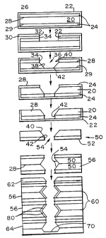
Fig. 1 illustrates the general flow diagram of a process for
micromachining discrete dynode electron multipliers according to
the present invention;
Figs. 2A and 2B depict respective fop plan and side sectional
views of a square aperture in .a Si wafer having the shape of a
truncated pyramid;
Figs. 2C and 2D depict respective top plan side sectional
views of a circular aperture in a Si wafer in the form of a truncated
hemisphere;
Fig. 3 is a side sectional elevation of a discrete dynode
electron multiplier according to an embodiment of the invention;
Fig. 3A is an enlarged fragmentary cross section of the
emissive surface shown in Fig. 3;
Fig. 4 is a side sectional elevation of a discrete dynode
electron multiplier according to an embodiment of the invention
employing an intermediate layer between aperture preforms;
Fig. 5 is a side sectional view of a discrete dynode electron
multiplier according to an embadiment of the invention employing
a resistive layer between dynode elements; and
Fig. 6 is a plot of gain versus applied voltage data for an
exemplary embodiment of the invention.
_3_
CA 02229731 1998-02-17
1
WO 97/05t~40 PCT/U596/12208
DESCRIPTION OF THE INVENTION
A general flow diagram of the process is shown in Fig. 1
depicting steps (a) - (h). The process begins at step (a) by forming '
a wafer 20 and generating a hard mask 22 thereon. It is preferable ,
to have a silicon wafer 20 of the n-type doped and as conductive as
possible (0.001 - 1.0 S2-cm). Wafers that are p-type doped may
also be useful to change the charge replenishment characteristics
of the dynode structure. Suitable hard mask materials include
polymers, dielectrics, metals and semiconductors. An exemplary
process employs a composite structure of Si02 forming an outer
isolation layer 24 produced by either direct thermal oxidation of the
silicon substrate 20 or by chemical vapor deposition (CVD); and
SiOYNx forming a hard outer layer 26 produced by CVD. The hard
mask 22 may employ one of these materials or it may be a
composite of these materials as depicted in the process described
herein. The composite hard mask 22 used in the exemplary
embodiment better preserves the cleanliness and flatness of the
respective top and bottom of the substrate wafer 20 for later
bonding.
At step (b) the hard mask is coated with a photo-sensitive
polymer or photoresist 30 and a pattern of one or more apertures 32
is generated in the photoresist 30 by optical lithography. Other
lithographic methods may be employed such as electron-beam, ion-
-4-
CA 02229731 1998-02-17
. ~ ,
WO 97/0540 PCT/CTS96/12208
beam or x-ray lithography. However, photolithography is readily
available and less expensive than other lithographic processes.
Regardless of how the pattern 32 is initially generated in the
photoresist 30, it is transferred as opening 34 through the hard
mask 22 by reactive particle etching (RPE).
In the process sequence illustrated in Fig. 1, the pattern
transferred to the hard mask 22 is a square opening 34. The size
for this opening 34 may be bet~nreen about 50 to 1000 Nm.
In step (c) an opening 36 is formed through the wafer 20 by
an anisotropic wet etch. The opening 36 shown in the process flow
diagram of Fig. 1 is the result of a potassium hydroxide (KOH)
applied to the Si wafer 20 in the [100] orientation. The side 38 of
the square opening 36 is aligned along the (111 ) plane so that there
is minimum undercutting of the hard mask 22. The result is an
aperture 36 having an enlarged opening 40 at the front face 28 and
a relatively smaller opening 42 at the back face 29. The opening or
aperture 36 through the wafer 20 has a shape of a truncated
inverted pyramid as depicted in Figs. 2A and 2B. Other openings
and etch systems may be employed. For example, a circular
opening 40 may be created with a Si etch such as HNA
(hydrofluoric-nitric-acetic acid). The resulting geometry of such an
etch is depicted in Figs. 2C and 2D and highlights the undercutting
of the hard mask resulting from an isotropic etch. In Figs. 2C and
.. 5 _
CA 02229731 1998-02-17
WO 97/05640 PCT/US96/12208
2D, the aperture or opening 40 has the shape of an inverted
truncated hemisphere.
Regardless of the exact geometry of the aperture through the
wafer, the remainder of the process is generally the same. After the
aperture in the wafer 20 has been formed in step (c), the outer
nitride layer 26 is removed from the front face 28 with a dry etch, as
shown in step (d).
In step (e), the underlying oxide layers 24 are removed from
the front face 28 and from the bottom opening 42 of the aperture 36
by an HF wet etch.
In step (f), the remaining nitride 26 is removed from the wafer
22 with hot (140-160°C) phosphoric acid (H3P04) which is highly
selective to both Si and Si02. The result is a dynode aperture
preform 50 having a resulting isolation layer 52 and a through
aperture 54 formed in the substrate 20. The isolation layer 52 is the
portion of the outer isolation layer 24, referred to above, remaining
after the various etch steps.
In step (g), a pair of dynode aperture preforms 50 are
assembled with the front faces 28 in confronting relation and the
apertures 54 aligned in registration, as shown. The dynode
aperture preforms 50 are then bonded, top face to top face, and
without an intermediate layer, to form one or more discrete dynode
- -6-
CA 02229731 1998-02-17
.
' WO'97/05640 PC'T/US96/I22ti8
elements 56. These are later activated to become active dynodes
as described hereinafter.
Bonding of the dynode aperture preforms 50 is generally
completed by direct fusion bonding. The technique requires the
surface of the components to be extremely flat, smooth and free of
particles. The clean surfaces are brought into contact and are
heated to a temperature in a range of about 600-1000°C for an
interval of about one to about three hours. This results in complete
bonding of the dynode aperture preforms 50 to form the discrete
dynode elements 56. In addition to direct fusion bonding, field
assisted bonding rnay also be employed.
In step (h), once the dynode aperture preforms 50 have been
bonded to form the discrete dynode elements 56, a number of such
discrete dynode elements are stacked together and bonded to
produce a discrete dynode stack 60, e.g., five or more dynode
elements. An input aperture 62, an output aperture 64 and an
anode G6 may be added to complete the stacked structure, as
shown in Figs. 1 and 3-5. Respective input and output apertures 62 ,
and 64 may each be an exemplary single dynode aperture preform
50, discussed above, which has been bonded to the stack 60.
It should be recognized that the dynode aperture preforms 50
may be directly bonded, top face to top face, with no intermediate
layer, as shown, when forming discrete dynode elements 56'.
_ _7_
CA 02229731 1998-02-17
i c
WO 97/05640 ' PCT/US96/12208 '
Alternatively, the dynode aperture preforms 50 may be separated
by an intermediate insulator layer, or a semiconductive layer 68, as
shown in the embodiment of Fig. 4.
Anode 66 may be an integrated structure constructed by the ,
same basic process as described above. The difference is
apparent in only one step of the process, namely step (c). The
KOH wet etch of the dynode aperture 36 is stopped before
penetrating the back side of the wafer 22, thereby leaving a bottom
surface 70 to collect the output electrons. The anode 66 may then
be bonded to the output aperture 64 to form the integrated
structure, as shown.
To activate the tapered surfaces 38 of the discrete dynode
elements 50, an electron emissive film 80, with good secondary
electron yield properties is employed, step (h), Fig 1 and Fig. 3A.
Generally, the film 80 is deposited on the surfaces 38 by low
pressure chemical vapor deposition (LPCVD) to a thickness of
about 2 to about 20 nm. Suitable materials include Si02 or Si3N4
although AIzO ~ AIN, C(diamond) or Mg0 may also serve as
excellent candidates. For examp9e, silicon nitride (SiNX) or silicon
oxynitride (SiNXOy) may be deposited with a combination of
dichlorosilane (SiCIZH2), ammonia (NH3) and nitrous oxide (N02) in
the temperature range of about 700 to about 900°C at a pressure
of about 100 to about 300 mtorr. Direct thermal oxidation could be
_g._
CA 02229731 1998-02-17
S 1
W0~97/0564b PCT/US96/I2208
carried out at about 800 to about 1100°C in dry 02 at atmospheric
pressure. Other methods for producing an electron emissive film 80
include atmospheric pressure chemical vapor deposition (APCVD)
and surface modification by thermal oxidation or nitriding
techniques.
A discrete dynode multiplier according to the invention may
be biased in one of two ways, direct or indirect. The most
conventional method of biasing these devices is the direct method.
This is shown in Fig. 3 by applying leads 82 to the discrete dynode
elements 56, the input aperture 62 and the anode 66 and
maintaining a potential at each element by means of an external
resistor network 84. The direct biasing technique is further
exemplified in Fig. 4 wherein different voltages may be separately
applied to each dynode aperture preform 50 forming the discrete
dynode element 56'. As noted above, each dynode aperture
preform 50 is separated from an adjacent preform by the insulating
inner layer 68. A disadvantage of the direct biasing technique,
illustrated in Figs. 3 and 4, is an increasing in the manufacturing
complexity and cost associated with the multiple electrical contacts
and multiple resistors. Also, this technique makes miniaturizing of
the device difficult.
The indirect method of biasing is illustrated in the
embodiment of Fig. 5, in which a discrete dynode electron multiplier
_g_
CA 02229731 1998-02-17
WO 97/05640 ' PCT/US96/IZZO8
90 employs an integrated resistor network. In this arrangement, a
semi-insulating or resistive layer 92 of an appropriate resistivity is
applied to the wafer 22 in step (a) depicted in Fig. 1. The film or '
layer 92 separating the discrete dynode elements 56 acts as a
resistor to allow the discrete dynode elements to be biased with
only a single electrical connection to the input aperture 62, the
output aperture 64 and the anode 66 through the device 90, as
shown. This allows for generally simplified manufacture and easier
miniaturization of the device.
The biasing depicted in Figs. 3 and 4 is configured for
collecting positive charged particles, neutral particles, UV-rays and
soft x-rays. This may be changed to a positive biased aperture, as
depicted in Fig. 5, to collect negatively charged particles (i.e., ions)
by floating the integrated anode 66 by means of an electrically
insulating layer 96 to allow the anode 66 to collect output current.
Floating of the anode 66 requires the insulating layer 96 to be
deposited on the anode even if intermediate resistive biasing layers
92 are employed.
An exemplary device manufactured by the process depicted
in Fig. 1, and biased as depicted in Fig. 4 has been constructed and
tested. The wafers 22 are each 380 microns in thickness, with a
front side opening to each dynode element of about 960 microns.
The device is indirectly biased and employs 12 discrete dynode
-10-
CA 02229731 1998-02-17
WO 97/05640 ' PCT/US96/I2208
elements. A plot of the gain of the device versus applied voltage is
shown in Fig. 6.
According to the invention, as illustrated in Fig. 3, an input
particle, e.g., an energetic electron, an ion, a UV photon, a x-ray or
the like 100 enters the input aperture 62 and produces a secondary
emission 102 which strikes the discrete dynode element 56
immediately there below, as shown. Additional secondary electrons
104 are produced which thereafter cascade to the next lower level
and on through the stack to the anode 66 as output electrons 106.
An output current to is thus produced which is indicative of the gain
of the device. Any number of stages may be employed, although it
is anticipated that about five to abaut twenty stages provide a useful
range of gain. The exemplary embodiment producing the data
illustrated in Fig. 6, employs 12 stages.
While there have been described what are at present
considered to be the preferred embodiments of the present
invention, it will be apparent to those skilled in the art that various
changes and modifications may be made therein without departing
from the invention, and it is intended in the appended claims to
cover such changes and modifications as fall within the spirit and
scope of the invention.
-11 -