Note: Descriptions are shown in the official language in which they were submitted.
CA 02233481 1998-03-27
z--,
Specification
Title of the Invention
Integrated Circuit Device Cooling Structure
Background of the Invention
The present invention relates to an integrated
circuit device cooling structure and, more particularly,
to an integrated circuit device cooling structure which
cools an integrated circuit device, which is packaged by
flip chip bonding called an area bump method or in a
ball grid array (BGA) package, with air by attaching a
heat sink to it.
Conventionally, in an integrated circuit
device cooling structure of this type, the integrated
circuit device is mounted on a wiring substrate such
that its lower surface faces the'upper surface of the
wiring substrate. A heat sink is attached to the upper
surface of the integrated circuit device.
Fig. 6 shows a conventional integrated circuit
device of this type. Referring to Fig. 6, a heat sink
26 is arranged on the upper surface of an integrated
circuit device 21. The lower surface of the heat sink
26 is fixed to the upper surface of the integrated
circuit device 21 so that it is thermally coupled to the
integrated circuit device 21. Heat generated by the
integrated circuit device 21 is transmitted to the heat
sink 26 and is radiated in the air.
- 1 -
CA 02233481 1998-03-27
Solder bumps 22 used for inputting/outputting
signals and connecting a power supply are formed on the
lower surface of the integrated circuit device 21. The
integrated circuit device 21 is not directly mounted on
a wiring substrate 25 but is mounted on an interposer
substrate 23 through the solder bumps 22. This is
because the solder bumps 22 has a small pitch and the
integrated circuit device 21 cannot be directly mounted
on the wiring substrate 25.
Solder balls 24 are arranged on the lower
surface of the interposer substrate 23. The solder
balls 24 are arranged at such a pitch that they can be
mounted on the wiring substrate 25. The interposer
substrate 23 is mounted on the wiring substrate 25
through the solder balls 24.
The prior art described above cannot cope with
an increase in power consumption that accompanies an
increase in operation speed and integration degree of
the integrated circuit device 21. To cope with an
increase in power consumption of the integrated circuit
device 21, the size of the heat sink 26 must be
increased, but the cooling performance does not increase
in proportion to an increase in size of the heat sink
26. To attach a large heat sink 26 to the integrated
circuit device 21, the attaching structure must also be
improved in accordance with the heat sink 26.
- ?. -
CA 02233481 2001-03-07
71180-154
Summary of the Invention
It is an object of the present invention to provide
an integrated circuit device cooling structure which can cope
with an increase in power consumption that accompanies an
increase in operation speed and integration degree of an
integrated circuit device.
It is another object of the present invention to
provide an integrated circuit device cooling structure which
can obtain a sufficiently large cooling effect by only
occupying a mounting region which is the same as or similar to
the outer shape of the integrated circuit device.
In order to achieve the above objects, according to
the present invention, there is provided a circuit device
cooling structure comprising: a first substrate; a circuit
device mounted on a first surface side of said first substrate;
a first heat radiation member fixed to a second surface of said
first substrate and thermally coupled to said first substrate;
a second heat radiation member fixed to a surface of said
circuit device that does not oppose said first substrate, and
thermally coupled to said circuit device; and a through hole
formed in said first substrate to transmit heat generated by
said circuit device to said first and second heat radiation
members.
Brief Description of the Drawincrs
Fig. 1 is a sectional view of an integrated circuit
device cooling structure according to the first embodiment of
the present invention;
3
CA 02233481 1998-03-27
Fig. 2 is a view showing a heat transmission
path in the integrated circuit device cooling structure
shown in Fig. 1;
Fig. 3 is a sectional view of a ball grid
array package type integrated circuit device cooling
structure according to the second embodiment of the
present invention;
Fig. 4 is a view showing a heat transmission
path in the integrated circuit device cooling structure
shown in Fig. 2;
Fig. 5 is a sectional view of a multi-chip
package type integrated circuit device cooling structure
according to the third embodiment of the present
invention; and
Fig. 6 is a sectlional view of a conventional
integrated circuit cooling structure.
Description of the Preferred Embodiments
The present invention will be described in
detail below with reference to the accompanying
drawings.
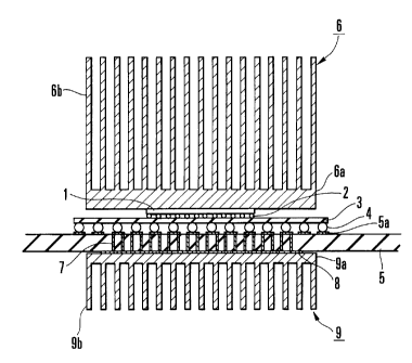
Fig. 1 shows an integrated circuit device
cooling structure according to the first embodiment of
the present invention. Referring to Fig. 1, the
integrated circuit device of this embodiment has a
wiring substrate 5, an integrated circuit device 1, heat
sinks 6 and 9, and a plurality of heat radiation vias 7.
Wiring patterns (not shown) are formed on the upper and
- 4 -
CA 02233481 1998-03-27
lower surfaces of the wiring substrate 5. The
integrated circuit device 1 is mounted on the upper
surface side of the wiring substrate 5. The heat sink 6
is fixed to the upper surface of the integrated circuit
device 1 to be thermally coupled to it. The heat sink 9
is attached to the lower surface of the wiring substrate
5 to be thermally coupled to it. The heat radiation
vias 7 are formed to extend through the wiring substrate
5.
The heat sinks 6 and 9 have rectangular bottom
plates 6a and 6b having the same size and a plurality of
fins 6b and 9b extending vertically from the bottom
plates 6a and 9a, respectively, and are monolithically
molded of aluminum. The central portion of the bottom
plate 6a of the heat sink ~ is fixed to the upper
surface of the integrated circuit device 1, and the fins
6b of the heat sink 6 are arranged to extend upward to
have a comb-like section. The bottom plate 9a of the
heat sink 9 is fixed to the lower surface of the wiring
substrate 5 through a heat radiation pad 8, as will be
described later, and the fins 9b of the heat sink 9 are
arranged to extend downward to have a comb-like section.
The heat radiation vias 7 are formed in a region of the
wiring substrate 5 that corresponds to the bottom plates
6a and 9a of the heat sinks 6 and 9.
A plurality of solder bumps 2 used for
inputting/outputting signals and connecting a power
_ 5 _
CA 02233481 1998-03-27
supply are arranged on the lower surface of the
integrated circuit device 1. Since the pitch of
arrangement of the solder bumps 2 is very small, an
interposer substrate 3 is interposed between the
integrated circuit device 1 and the wiring substrate 5.
This is because the miniaturization of the wiring
pattern of the wiring substrate 5 cannot catch up with
the bump pitch and the integrated circuit device 1
cannot be mounted on the wiring substrate 5 directly.
The integrated circuit device 1 is mounted on
the upper surface of the interposer substrate 3 through
the solder bumps 2, and the interposer substrate 3 is
mounted above the wiring substrate 5 to oppose its upper
surface. The interposer substrate 3 is connected to the
wiring substrate 5 through solder balls 4 that are
arranged on the lower surface of the interposer
substrate 3 at such a pitch that they can be mounted on
the wiring substrate 5. Wiring patterns (not shown) are
formed on the two surfaces of the interposer substrate
3, and the solder bumps 2 and the solder balls 4 are
electrically connected to each other through these
wiring patterns.
The interposer substrate 3 has a square shape
with sides each having a size of about S cm. The
interposer substrate 3 is made of a ceramic material,
and more particularly, alumina or aluminum nitride. If
the solder bumps 2 of the integrated circuit device 1
_ 5 _
CA 02233481 1998-03-27
can be directly connected to the pattern of the wiring
substrate 5, the interposer substrate 3 is not required.
The wiring substrate 5 has a plurality of pads
5a arranged at positions opposing the plurality of
solder balls 4, the plurality of heat radiation vias 7,
and an internal wiring. The wiring substrate 5 has a
thickness of about 3 mm to 3.5 mm and a size of about
12 cmz to 13 cmz. The material of the wiring substrate 5
is an epoxy or polyimide resin.
The heat radiation vias 7 transmit heat
generated by the integrated circuit device 1 mounted on
the upper surface side of the wiring substrate 5 to the
lower surface of the wiring substrate 5. The heat
radiation vias 7 are arranged in a matrix. Preferably,
through holes constituting'the heat radiation vias 7 are
filled with a solder having a high thermal conductivity.
In this case, the thermal conductivity can be further
improved when compared to a case wherein nothing fills
the heat radiation vias 7. The diameter of each heat
radiation via 7 is 0.3 mm to 0.4 mm. The heat radiation
vias 7 are arranged to be displaced from the solder
balls 4 arranged on the interposer substrate 3 so that
they are not electrically connected to them.
The heat sink 6 is attached to the upper
surface of the integrated circuit device 1, i.e., to a
surface opposite to a surface where the solder bumps 2
are formed. More specifically, the heat sink 6 is fixed
_ a _
CA 02233481 1998-03-27
to the upper surface of the integrated circuit device 1
by using an adhesive obtained by mixing device heat
conductive filler particles, e.g., a metal oxide, in an
epoxy or silicone resin, or by a low-melting metal,
e.g., a solder. The heat sink 6 may be urged against
the integrated circuit device 1 with a force of springs
or screws. In this case, if a grease-type heat
conductive material is applied to the contact surface
between the heat sink 6 and integrated circuit device 1,
thermal coupling between the heat sink 6 and integrated
circuit device 1 can be made more firm.
The heat radiation pad 8 is arranged on the
lower surface of the wiring substrate 5, i.e., on a
surface opposite to a surface where the integrated
circuit device 1 is mounted. The heat radiation pad 8
is formed in the process of forming the wiring pattern
on the lower surface of the wiring substrate 5, and
requires a size to include at least the plurality of
heat radiation vias 7. The heat sink 9 is attached to
the heat radiation pad 8 arranged on the lower surface
of the wiring substrate 5. The heat sink 9 is fixed to
the heat radiation pad 8 in the same manner as that with
which the heat sink 6 is fixed.
The operation of the integrated circuit device
cooling structure having the above arrangement will be
described with reference to Fig. 2. Referring to
Fig. 2, heat generated by the integrated circuit device
_ g _
CA 02233481 1998-03-27
1 is radiated from both the upper and lower surfaces of
the integrated circuit device 1 along first and second
transmission paths A and B.
The first transmission path A consists of the
integrated circuit device 1 and the heat sink 6. Heat
generated by the integrated circuit device 1 is
transmitted in the integrated circuit device 1 to the
heat sink 6 from the upper surface of the integrated
circuit device 1, and is dissipated in the air through
the bottom plate 6a and fins 6b of the heat sink 6.
The second transmission path B consists of the
integrated circuit device 1, the solder bumps 2, the
interposes substrate 3, the solder balls 4, the pads 5a,
the wiring substrate 5, the heat radiation vias 7, the
heat radiation pad 8, and the heat sink 9. Heat
generated by the integrated circuit device 1 is
transmitted to the interposes substrate 3 through the
solder bumps 2, and to the wiring substrate 5 through
the solder balls 4 and the pads 5a. Heat transmitted to
the wiring substrate 5 is transmitted to the heat
radiation pad 8 through the wiring substrate 5 itself
and the heat radiation vias 7, is then transmitted from
the heat radiation pad 8 to the bottom plate 9a and fins
9b of the heat sink 9, and is dissipated in the air.
In this manner, in this embodiment, the heat
sink 9 is arranged on the surface of the wiring
substrate 5 where the integrated circuit device 1 is not
_ g _
CA 02233481 1998-03-27
mounted, and the plurality of heat radiation vias 7 are
arranged in the region of the wiring substrate 5 where
the heat sink 9 is mounted. Hence, heat resistance in
transmitting heat from the integrated circuit device 1
to the heat sink 9 through the wiring substrate 5 can be
decreased.
This embodiment has two heat transmission
paths, i.e., the first transmission path A on the upper
surface side of the integrated circuit device 1 and the
second transmission path B on the lower surface side of
the integrated circuit device 1. Therefore, this
embodiment can cope with an increase in power
consumption that accompanies an increase in operation
speed and integration degree of the integrated circuit
device 1.
In this embodiment, the heat radiation pad 8
is arranged between the wiring substrate 5 and heat sink
9. However, the heat radiation pad 8 can be omitted.
In this case, the heat sink 9 is attached directly to
the wiring substrate 5.
In this embodiment, the heat radiation vias 7
and the solder balls 4 are located to be displaced from
each other. However, the present invention can include
an arrangement in which the heat radiation vias 7 and
the solder balls 4 are electrically connected to each
other. In a more preferable example, a specific heat
radiation via 7 electrically connected to a specific
- 10 -
CA 02233481 1998-03-27
solder ball 4 is used as an electrode for the power
supply or GND.
The second embodiment of the present invention
will be described in detail with reference to Fig. 3.
The characteristic feature of the second embodiment
resides in that the integrated circuit device is
packaged in a ball grid array (BGA) package. Except for
this, the arrangement of the second embodiment is
identical to that of the first embodiment.
Referring to Fig. 3, an integrated circuit
device 10 is packaged in a BGA package 11. The
integrated circuit device 10 is mounted such that its
surface opposite to the circuit surface opposes the
upper surface of the BGA package 11. The input/output
terminals of the circuit surface of the integrated
circuit device 10 and the electrodes on the upper
surface of the BGA package 11 are connected to each
other by wire bonding. The integrated circuit device 10
is sealed in the BGA package 11 with a resin.
Solder balls 12 are arranged on the lower
surface of the BGA package 11 to electrically connect
the BGA package 11 and a wiring substrate 13 to each
other. A heat sink 16 is fixed to the upper surface of
the BGA package 11 so as to be thermally coupled to the
package 11. The outer shapes (of the bottom plates) of
the heat sink 16 and of a heat sink 17 have almost the
same size as that of the BGA package 11. The size of a
- 11 -
CA 02233481 1998-03-27
region of the wiring substrate 13 where heat radiation
vias 14 and a heat radiation pad 15 are formed also has
almost the same size as the outer shape of the BGA
package 11.
The operation of the integrated circuit device
cooling structure having the above arrangement will be
described with reference to Fig. 4. Referring to
Fig. 4, heat generated by the integrated circuit device
is radiated along first and second transmission paths
10 A and B.
In the first transmission path A, heat
generated by the integrated circuit device 10 is
transmitted to the heat sink 16 through the sealing
resin of the BGA package 11, and is then dissipated in
the air.
In the second transmission path B, heat
generated by the integrated circuit device 10 is
transmitted in the integrated circuit device 10 and BGA
package 11, and is transmitted to the wiring substrate
13 through the solder balls 12 and pads 13a. Heat
transmitted to the wiring substrate 13 is transmitted to
the heat radiation pad 15 through the wiring substrate
13 itself and the heat radiation vias 14, is then
transmitted from the heat radiation pad 15 to the heat
sink 17, and is dissipated in the air.
In this manner, .in this embodiment, the
integrated circuit device .10 of the BGA package 11 can
- 12 -
CA 02233481 1998-03-27
be sufficiently cooled by only mounting the heat sinks
16 and 17 on regions having sizes substantially equal to
that of the outer shape of the BGA package 11.
The third embodiment of the present invention
will be described in detail with reference to Fig. 5.
The characteristic feature of the third embodiment
resides in that the arrangements of the first and second
embodiments described above are applied to a multi-chip
module (MCM).
Referring to Fig. 5, a MCM 100 is constituted
by mounting a microprocessor chip 18 and cache memory
chips 19 on a wiring substrate 20. Since the
microprocessor chip 18 has a comparatively large number
of input/output signals, it is packaged by flip chip
bonding. The cooling structure for cooling the
microprocessor chip 18 preferably employs the first
embodiment shown in Fig. 1.
Since the cache memory chips 19 are mass
production products, they are packaged by using BGA
packages that are standard packages. The cooling
structure for cooling the cache memory chips 19 can
employ the second embodiment shown in Fig. 3.
As the performance of the information
processing apparatus in which the MCM 100 is packaged is
more and more improved, the operation speed and
integration degree of the integrated circuit device are
increased. In this case, sometimes the microprocessor
- 13 -
CA 02233481 1998-03-27
chip 18 consumes power of several W to 30 W, and even
the cache memory chips 19 consume power equal to or
larger than 1 W. In this embodiment, heat generated by
this high power consumption can be efficiently removed.
In this embodiment, heat sinks are separately
arranged on the upper surfaces of the microprocessor
chip 18 and cache memory chips 19 and the lower surface
of the wiring substrate 20 on which the microprocessor
chip 18 and cache memory chips 19 are mounted, i.e., on
a surface of the wiring substrate 20 where the
microprocessor chip 18 and cache memory chips 19 are not
mounted. Hence, large-size heat sinks need not be
employed. As a result, a change in arrangement of the
respective chips on the MCM 100, which is required when
attaching large-size heat sinks, is not needed.
In the respective embodiments described above,
the heat radiation vias are formed only in the wiring
substrate. However, heat radiation vias may be formed
in the interposes substrate as well so that a higher
thermal conductivity can be obtained.
As is apparent from the above description,
according to the present invention, heat generated by
the integrated circuit device is transmitted to the heat
sink arranged on the lower surface of the wiring
substrate through a plurality of heat radiation vias
formed in the wiring substrate. Therefore, heat
- 14 -
CA 02233481 1998-03-27
resistance in transmitting heat from the integrated
circuit device to the heat sink can be decreased.
Since the present invention has, as the heat
transmission path for removing heat generated by the
integrated circuit device, the first transmission path
for transmitting heat to the first heat sink arranged on
the upper surface side of the wiring substrate, and the
second transmission path for transmitting heat to the
second heat sink arranged on the lower surface side of
the wiring substrate, the entire heat radiation amount
increases. As a result, heat generated by the
integrated circuit device can be removed effectively,
coping with an increase in power consumption that
accompanies an increase in operation speed and
i
integration degree of the '.integrated circuit device.
- 15 -