Note: Descriptions are shown in the official language in which they were submitted.
CA 02241823 1998-06-29
W O 97131288 PCT~US97/00369
MICROMECHANICAL OPTICAL SWITC~ AND FLAT PANEL DISPLAY
Government Ri~Jhts in the In~ention
s This invention was made with U.S. Government support under Contract Number
F196Z8-90-C-002 awarded by the Air Force. The U.S. Government has certain rights in
this invention.
Field of the Invention
This invention relates to optical switching techniques. and more particularly
lo relates to optical switching in large-scale optical systems such as optical displays.
Back~round of the Invention
Electronically con~rolled optical displays. and particularlY flat panel optical
displays, which generally are distinguished by their relative ~limne~c and ability to
produce a direct. as opposed to a pro3ected. display image are of increasing
teehnologieal importanee for a wide range of applieations. Flat panel optical displays
that produee direetly viewable video images such as text and graphics are in theory
ideally suited as television monitors, computer monitors. and other such display screen
seenarios. Yet the many flat panel optieal display approaehes hereto~ore proposed and
investi~t~-i all exhibit serious disadvantages that have limited their praetiealapplicability as a commercially viable flat panel display screen technology.
For example. the class of flat panel displays known as liquid erystal displays
require eomplex manufaeturing proeesses that eurrently produee relatively low yields,
resulting in an overall size limitation for volume produetion. ln operation. Iiquid erystal
displays require considerable power to mzlintzlin a display k~rklight and these displays
provide only a limited range of viewing angles. ~:leetrolumineseent display teehnology
suffers from similar limitations. as well as a limited display color range and limited
operational lifeeycle.
Aetive-matrix display technology, which employs an acti-~e eleetronic deviee at
eaeh pixel loeation of a display. is likewise limited both by high power consumption,
produetion yield eonstraims. and limited operational lifeeyele. Color ~as plasma display
teehnology, like liquid crystal teehnology, requires a complex m~?nuf~cturing proeess to
CA 02241823 1998-06-29
W O 97131288 PCT~US97/00369
produce an optical display; a gas plasma display relies on complicated p~k~ging
s~ h~mPs for providing reliable cQnt~inment of a noble gas~ resulting in high
m~nnf~cturing costs.
Various electromeçh~nic~l display technologies have been proposed which
generally rely on electronic control in conJunction with manipulation of mechanical
elements in a display. Typical mechanical display sch~n~s have been limited by so
many m~nuf~rtl-ring complexities and/or operational constraints that they are as yet
commercially impractical. Furtherrnore. the speed, resolution~ and po~ er consumption
uil~ ents of the latest optical display applications have heretofore been unachievable
lo by conventional electromechanical display technologies. But electronic as well as
electromech~nical display technologies have all re~uired design and perforrnance trade-
offs resulting in one or more suboptimal m~nllf~cturing or operational considerations.
Summarv of the ~nvention
The invention provides an optical coupling switch and optical displav employing
15 an array of optical coupling switches that overcome limitations of past optical switches
and displays to achieve superior display switch speed, display efficiencv. compact
geometry~ and ease of m~nuf~cture. The optical coupling switch of the invention
includes a light storage plate that is adapted to set up conditions for total intelnal
reflection such that light injected into the plate is internally reflected .~ Iight tap is
20 disposed proximal lo a coupling surface of the light storage plate for coupling internally
reflected light out of the light storage plate and into the light tap when ~he light lap is
brought into contact with the light storage plate coupling surface. The light tap is
capable of movement in a direction perpendicular to the light storage plate in ~ o,~se
to an applied electrostatic force. The optical coupling switch also includes a sc~rin~
25 merhs3ni.~m such as a sc~LL~;~hlg surface or scattering medium. for sC~ttprin~ light in the
light tap. With this configuration. the optical coupling switch provides an elegantly
uncomplicated geometry that accommodates a range of actuation schemes for efficiently
producing high-speed optical switching. ~,
The light coupled into the light tap is effectively scattered bv the scattering
30 m-orh~ni~m such that a practical range of optical viewing angles is produced by the
CA 02241823 1998-06-29
W O 97/31288 PCT~US97/00369
optical coupling switch. In preferred embodiments. the scattering mechanism of the
. optical switch is a scattering surface, preferably on the light tap. and includes. e.g.,
surface asperities or a surface grating. In other preferred embodiments. the scattering
m~-hz~ni~m is a scattering medium that is translucent. fluorescent. or l-lmin~ scent.
Preferably, the light storage plate includes at least one coupling mesa located on
the coupling surface in correspondence with the light tap such that the light tap contacts
at least one coupling mesa when brought into contact with the light storage plate.
~lt~ tively at least one coupling mesa is preferably located on the light tap and is in
contact with the light storage plate when the light tap is brou~ht into contact with the
o light storage plate.
In preferred embollimentc~ the li~ht tap is characterized by an internal
m~ch~nical restoring force. e.g.. a tensile or compressive force. that opposes applied
ele~ o~lic force. Preferably the light tap is mechanically biased either into or out of
contact with the light storage plate by this mechanical restoring force. and is moved in
the other direction. i.e., out of or into contact with the light storage plate. bv an applied
electrostatic force. Alternatively, the light tap is both biased and moved into and out of
contact with the light storage plate by an applied electrostatic force.
Preferably. the light tap of the optical coupling switch includes a textured
Larnbertian scattering surface that is reflective for reflecting coupled light back through
the light storage plate to emerge into a viewing volume adjacent to the light storage
plate. Alternatively. the sC~tterin~ surface on the light tap is a forward Sc~LL~ing surface
for s~ L~ g coupled light into a viewing volume adjacent to the light tap. In this case,
a viewing plate is preferably disposed adjacent to the light tap. The viewing plate can
also include a scattering surface for sÇzlttering light that emerges through the viewing
plate into a viewinY v olume adjacent to the viewing plate. A light source is preferably
located at an edge of the light storage plate.
The light tap is preferably anchored to the viewing plate by at least one support
" located at a point on the tap that perrnits flexing of the tap. and the viewing plate is
preferably secured to the light storage plate. Preferably. the light tap includes
protrusions on a surface facing the light storage plate. These protrusions perrnit
CA 02241823 1998-06-29
W O 97131288 PCTAUS97/00369
coupling of light into the light tap but suppress contact forces between the light tap and
the light storage plate. ..
In preferred embo~1iment~. two or more of the light tap, viewing plate, and light
storage plate include a c(lnd~ ting electrode disposed in correspondence with each other ''
for generating an electrostatic force. Alternatively. the light tap includes a con-lllctin~
electrode and the viewing plate or light storage plate include an electret for gencLdtillg
an electrostatic force.
Preferably, the light storage plate is forrned of a glassy material such as quartz,
or is formed of plastic. The light tap is preferably formed of a microelectronic material
] o such as plastic or silicon nitride, and the viewing plate is preferably formed of plastic or
a glass material. such as quartz.
In another aspect, the invention provides an optical display in which an array of
light taps are disposed proximal to a light storage plate coupling surface. Each light tap
is adapted to move in response to an applied electrostatic force in a direction
perpendicular to the coupling sllrf~ e. and each light tap includes a scattering surface for
scaLL~ ng coupled light. A light source is disposed at an edge of the light storage plate
for injecting light into the plate. Control circuitr~ is provided connected to the array of
light taps for applying an electrostatic force to selected one or more of the light taps in
the array.
In preferred embodiments. a viewing plate is disposed adjacent to the light tap
array, and the viewing plate includes an array of electrodes disposed on the viewing
plate in correspondence with electrodes on the taps in the light tap array for producing
an electrostatic force. Preferably, the control circuitry includes line and column
electrode drive circuits and a controller for applying an electrostatic force between
2s selected one or more of light tap and viewing plate electrodes in the array.
Preferably, the light source is configured ad~acent to an edge of the light storage
plate such that light in~ected into the light storage plate undergoes total int~reflection. A second light source can be disposed at an edge of the light storage plate
and a second light source can be disposed on the back surface of the light storage plate.
Preferably~ the light source produces at least two different colors of light.
CA 02241823 1998-06-29
W O 97/31288 PCTn~S97/00369
In yet other preferred embodiments. the array of light taps forms an array of
pixels. each pixel ~lecign~tec~ by a set of n light taps corresponding to a number n of
pixel bits. Each of the n light taps in the given pixel is controlled by the control
~I ch'cuilly to together produce for a given pixel one of a number of 2" of possible optical
5 i ~ s Preferably, each of the n light taps in a given pixel is adapted to make
contact with a contact area of the light storage plate havin~ one of a number n of
possible contact area sizes for a given pixel. Alternatively~ the number ~ of pixel bits
for a given pixel is the product of a temporal weight t e~ual to a number of possible
durations during which light is injected into the light storage plate and an area weight w
o e~ual to a number o~possible contact area sizes in a given pixel.
Preferably. the light tap array is formed of a plastic laver disposed proximal to
the light storage plate. which in this case is also preferably plastic and is characterized
by a refractive index such that light injected into the plate is internally reflected. The
viewing plate is then also preferably plastic. The light taps are here formed of an array
15 of conclucting column electrodes disposed on the plastic sheet; ~LLr~l~bly, an array of
slots border the column electrodes. The plastic viewing plate includes an array of
conll~]ctin~ line electrodes located in correspondence with the column electrodes on the
plastic sheet for producing an electrostatic force. Preferably. the plastic light storage
plate includes spacer protrusions for holding the plastic sheet separated from the light
20 storage plate and similarlv. the plastic viewing plate includes support protrusions for
holding the plastic sheet separated from the viewing plate.
The optical coupling switch configuration of the invention can be employed in a
wide range of display architectures, as well as other optical switch-based applications.
Television displays~ table top computer displays and other computer displays, monitor
25 displays, kiosks, equipment monitors. and the like all achieve superior design and
perfo~nance with the invention due to the flat. compact configuration of the display and
the low power ~iccip~tion achieved by the actuation and control sche~ec.
Aside from display applications, the optical coupling switch configuration of the
invention can also be used. for exarnple. in applications such as optical relay or circuit
30 breaker systems. two-~iimencional digital optical computing. and other such optical
CA 02241823 1998-06-29
W O 97131288 PCTrUS97/00369
switch applications. For example. the mechanical tap configuration can be employed to
selectively radiate energy from an array of waveguides, wherebv a single pole-multiple
throw optical switch is produced. Optical multiplexing and opto-isolation s~ht?mPs are
accordingly enabled by the invention. Other features and advantages of the invention
5 wil~ be ~ lt from a description of a preferred embodimem. and from the claims.Brief De~ ion of the Drawin~s
Figure I is a perspective view of an example flat panel display in accordance
with the invention,
Figure 2 is a schematic diagram showing an edge of the flat panel display of
0 Figure 1 and a possible path of light injected into the display;
Figure 3A and Figure 3B are schem~tic side views of an example optical switch
in accordance with the invention;
Figure 3C is a srhPm~tic side view of a second exarnpie optical switch in
accordance with the invention;
~5 Figures 4A-4B are srhPm~tic side views of a third exarnple optical switch in
accordance with the invention;
Figures ~C-4D are s~hPn~tic side views of a fourth example optical switch in
accordance with the invention;
Figure 4E is a schem~tic side view of a fifth example optical switch in
~o accordance with the invention:
Figure 5 is a sc~Pn~tic side view of a sixth example optical switch in accordance
with the invention,
Figure 6A is a srh~m~tic side view of a mechanical tap employed in the optical
switches of Figures 4A-4E and Figure S and having a Lambertian scattering surface in
25 accordance with the invention;
Figure 6B is a sçhP-m~tic side view of a mech~nical tap empioved in the optical
switches of Figures 4A-4E and Figure ~ and having a color surface in accordance with
the invention;
CA 02241823 1998-06-29
W O 97131288 PCTrUS97/00369
Figure 7 is a plot of optical mechanical switch position as a function of applied
potential difference for a mechanical tap control scheme in accordance u-ith the
invention;
~Y Figure ~A is a schem~tic back-side view of a flat panel display in accordance
with the invention;
Figure 8B is a s. hem~tic cross sectional view of the flat panel display of Figure
8A taken through the line 8B-8B';
Figure 8C is a schematic back-side view of the flat panel display of Figure 8A
with the light storage plate of the display removed;
0 Figure 9 is a sch~m~tic plot of the switch state of optical m~ h~nical switches in
an array of such switches controlled by an example set of voltages in accordance with
the control scheme plotted in Figure 7;
Figure lOA is a plot of colors displayed in an exarnple sequence of color time
slots in a display frame in acco.d~ulce with the invention;
1S Figure lOB is a plot of an exarnple optical switch actuation and color flash
timing sequence for producing the color sequence of Figure I OA;
Figure I OC is a schPm~tiC temporal and spatial plot of an example display line
eleckode actuation sequence for producing the timing sequence of Figure 1 OB,
Figure 11 is a schematic view of an example flat panel display pixel including
eight optical met~hsmical switches in accordance with the inven~ion;
Figure 12A is a sch~Pm~tic view of a line electrode driver circuit in accordancewith the invention;
Figure 12B is a srh~m~tic view of a column eleckode driver circuit in
accordance with the invention;
2~ Figure 1 2C is a schematic view of a single-pole~ double-through switch in
accordance with the invention for use in the line and column electrode driver circuits of
Figures 1~A and 12B;
Figure 13A is a schPm~tic side view of an optical prism wedge configured with a
light storage plate in accordance with the invention ~or injecting light into the light
storage plate:
CA 02241823 1998-06-29
W O 97131288 PCTrUS97/00369
Figures 13B and 13C are schematic diagrarns illustrating geometric
considerations for positioning a flash lamp line source in relation to a parabolic reflector
for producing an optical source in accordance with the invention,
Figure 14 is a sch~m~tic view of an example color optical source and its
configuration with an edge of a light storage plate in accordance with the invention;
Figure 15 is a schematic view of an example optical source and its configurationwith the back surface of a light storage plate in accordance with the invention;Figure 16 is a schematic view of an array of the example optical sources of
Figures 14 and 15 configured with a light storage plate in accordance with the invention.
o Figures 17A-17K are schematic side views illustrating fabrication steps for a
first flat panel display m~n~ turing process in accordance with the invention;
Figures 1 8A-1 8G are schematic views illustrating fabrication steps for a second
flat panel display m~nllf~t~.turing process in accordance with the invention; and
Figure 19 is a schematic side view of a seventh example optical switch in
accordance with the invention.
Descril~tion of a Preferred Embodiment
As shown srhem~tically in Figure 1, a flat panel display 10 provided by the
invention operates to controllably release light stored in a l~ls~al~nt light storage plate
12 for producing a localized viewable pattern of light on the display. Light is provided
2Q to the storage plate 12 by a light source 14, which injects light 16 into the storage plate.
This injected light is shown only schematically at the edge of the storage plate in Fig. 1.
The injected light remains substantially trapped in the storage plate due to a prespecified
condition of total internal reflection. However, the display includes mechanical light
taps, (not shown) corresponding to a matrix of locations along the storage plate, that
provide the ability to overcome the total internzll reflection condition at the light tap
locations such that light is released from the storage plate toward a viewer at distinct
locations, e.g., the location identified as 18 in Fig. 1. This controlled release of light
enables the production of a viewable image across the storage plate. The features and
operation of the light storage plate, the mechanical light taps, and the other elements of
the flat panel display will be explained in turn below.
CA 02241823 1998-06-29
W O 97/31288 PCTAUS97/00369
The light storage plate 12, shown on-ed~ e in Fig 2. communicates with the lightsource 14, which may include multiple sources 14a. 14b. located at one or more edges of
~e plate. such that light, preferably co11im~te~l is injected into the plate Collimators
'J 20a, 20b, or other suitable schemes can be employed to achieve a desired collimation.
5 Details of specific light source configurations will be described later in the discussion.
Once injected in the storage plate~ light 16 impinges on surfaces of the plate. bouncing
from one surface to the other parallel surface. At each such bounce. the light impinges
the cull~,s~uollding surface at an angle of internal incidence. ~" as measured with respect
to the perp~ntli~ r 22. At the point of the bounce. a component of the light bounces
10 back toward the other surface at an angle ûf reflection - ~,. and a component of the light
emerges out of the plate from the bounce surface at an angle of emer~ence. f~e
For a given internal incidence angle, t~, Snell's law prescribes both the angle of
reflection. -~,. and the angle of emergence. ~e~ as measured with respect to thepe~p~n~lirl~l~r 22 of a storage plate surface, as shown in Fig. 2, as:
njsin~ esin~9e~
where nj is the index of refraction in~ernal to the storage plate and ne is the index of
refraction external to the storage plate A configuralion of the light injected into a
storage plate such that the value of ~j in Snell's law results in a minimllm value for ~c of
90~ prescribes that no light emerges from the storage plate. but rather. is substamially
20 entirely reflected back at the reflection angle -~, to the opposite surface: this condition is
known as total internal reflection The minimum incident internal critical angle, ~ c,
that enables this condition is in turn defined by Snell s law as:
sin~C = neln~. (2)
One example storage plate in accordance with the invention is made of quartz; in2s this case the internal index of refraction. nj, is that of the quartz. namely, about 1.47.
Given that the flat panel display is typically operated in accordance with the invention in
air, the external index of refraction. n~, is about 1.00~ and correspondence (2) above sets
~c equal to about 42.9~ Any internal incidence angle. ~" larger than about 42.9~ results
in an im~gin~ry value for the angle of emergence. ~.. whereby the light undergoes total
CA 02241823 1998-06-29
W O 97131288 PCT~U~97/00369
~ 10
int~rn~i reflection within the quartz plale: stated another wav. under this condition ligh~
emerging externally to the plate could not propagate~ and instead would decay
exponentially in the rli.ct~nce normal to the plate. Thus~ light injected into the quartz
storage plate at angles greater than about 42.9~ does not emer~e from the plate each time
5 it strikes an internal surface of the plate~ and instead bounces back off internal plate
surfaces. As a result. the light cannot effectively be seen bv a ~ iewer even though the
plate is ~ ,nl.
Based on this ~ cllc~ion of total internal reflection. the storage plate 12 of the
flat panel display is generally specified as a transparent material having a high index of
o refraction relative to air and a suitable absorption loss for a given application. Examples
of suitable materials other than ~uartz include other ~vpes of clear glasses. plastics. e.g..
PlexiglassTM, polystyrene. and like materials. The thickness of the storage plate is
preferably selected based on considerations for a given application; the thickness of the
plate as well as the lateral plate Aimen~ions. determines the number of internal15 reflection bounces that occur for a light beam as it traverses the extent of the plate. A
thickness of ~ e.g., between about lrnm and 10 rnm is suitable for many applications. but
the th~cknlos~ can be larger or smaller than this range. Specific storage plate
m~ r~ ring considerations will be addressed in detail later in the discussion.
~ight is said to be ~stored" in the light storage plate 12 as a result of ~ nment
20 of components in the light source 14 with the storage plate such that light is injected at
an angle sufficient for total internal reflection of the light in the plate. This stored light
is controllably released. or tapped~ in accordance with the invention. at distinct locations
of the storage plate by bringing one or more mechanical light tap elements 24. an
example of which is shown in cross section in Figs. 3A-3B. in contact with the storage
2~ plate. The region in which light is released by a light tap element ~4 is defined by a
light storage plate contact area. i.e.. the area of the storage plate that is contacted when a
tap element is brought into contact with the plate. ~n one example. such a contact area
consists of a mesa 26 on one of the surfaces of the storage plate 12.
The mechanical tap is preferably formed of. e.g.. a suspended beam 28
L~ L to the optical wavelengths of interest and having a smooth front surface 30
CA 0224l823 l998-06-29
W O 97t31288 PCT~US97/00369
adjacent the mesa and a reflective back-scatter surface 32 on a side opposite the mesa.
The mechanical tap is preferabl,v of a high index of refraction relative to the index of
refraction of air. and most preferablv is of an index of refraction equal to or greater than
that of the light storage plate.
When the mer,h~nical tap is held separated from a storage plate mesa~ iight 16 in
the storage plate remains trapped in the storage plate due to total internal reflection.
Movement of the mechanical tap into close contact with the top surface 34 of a
corresponding storage plate mesa results in relative m~trhing of the imernal index of
refraction of the storage plate and the index of refraction external to the storage plate at
0 the location of the storage plate contact area~ for example. the mesa top surface.
compared to other surface locations of the storage plate: this condition negates the state
of total internal reflection at the location of the contact area and results in escape of light
from the storage plate 1~ into the suspended beam. or mechanical light tap 28~ as shown
in Fig. 3B.
Light escaping imo the merh~nical tap propa~ates through the thickness ofthe
tap and impinges on the reflective back-scatter surface 32 of the tap. ~here the light is
reflected ~aclc through the tap toward the light storage plate and into the storage plate.
The surface irregularities of the back-scatter surface 32 preferably are of a geometry
such that light re-en~ering the light storage plate 12 is angled. once in the plate. at an
~o angle less than the critical angle. OC. defined by Snell's law for the gi~en storage plate '
material. With this geometry. the re-entering light 3~ impinges the front surface 36 of
the storage plate I '~ at an angle insufficient to support total internal reflection of the
light, wherebv the light 35 emerges from the front surface 36 of the storage plate and
can be seen by a viewer.
As explained in detail below. this localized light release scheme provides a high-
speed displav configuration that is highly efficient and that provides for superior
contrast. brightnecs resolution. and dynamic range. A flat panel displa ~ enabling such a
srh~me. in accordance ~ith the invention. is compact. durable. easily manufactured, and
of reasonable materials and manufacturing costs. These advantages ~-ill be highli~hte~
3~ in the relevant discusslon to follow.
CA 02241823 1998-06-29
W O97/31288 PCT~US97/00369
In an alternative light release scheme. shown in Fig 3C. the mechanical light tap
is embodied as a transparent suspended beam 78 havinc a transparenl back surface 32 of
a geometry that results in forward-scattering, rather than back-scattering. of light
impinging the surface. In this case, light 16 that escapes from a mesa 26 in the light
s storage plate into a light tap 28 in close contact with the mesa propagates through the
thickness of the light tap and out the back surface 32 of the tap 28 The surfaceirregularities of the back surface 32 are preferably of a geometry such that light emerges
from that surface and is scattered in a reasonable angle of viewable emergent light.
Considering now the m~gnitll-le of movement required of a mechanical Iight tap
o to effect a distinct "on' and "ofr' of display light emerging from the light storage plate,
the phenomenon of evanescent light coupling must be evaluated for the mechanical tap
geometry. The eV~n~scent light amplitude. f~. of light coupled out of a free surface of a
transparent medium cont~ining total-internally-reflected light into an external medium.
e g., air. in which an element of similar refractive index to that of the light source is
positioned, is given approximately as:
Ee = Eje~'~, (3
where ~; is the incident light level at the free surface. _ is the perpendicuiar ~lict~n~e, in
the air. awav from the free surface. defined in Fig. 2~ and a is an expression given as:
a = (27~/~ j) [sin ~, -( ne/n,)
where al, ne~ and nr are ~iven as in Fig. 2 and ~, is the wavelength of light imernal to the
Ll~1s~ c~lL medium These ~ s~ions indicate that evanescent light coupling decaysexponentially at a rate defined by a: the expressions ignore the effects of polarization
and ignore the effects of the adjacent mechanical tap surface proximity
For the exarnple described above in which the light storage plate is forrned of
~uartz and the display is operated in air, n~ = 1 00 and ni= 1.47 Given an intl?rn~l
inr:i~ent light angle of 50~ (which accommodates total internal reflection in the ~uartz
plate) and a midband ~avelength of light in the plate of. e.g., about 0.55 um. expression
(4) above for a provides a value of ~ ~ 5.91 /!lm This ~ value~ when used in
expression (3) abo~e. indicates that the evanescent light amplitude. E~, is reduced to
CA 02241823 1998-06-29
W O 97131288 PCTAUS97/00369
about 30 dB below the incident light amp}itude. ~? at a distance of about 0.58 ~lm from
the surface of the storage plate. In other words. midband evanescent light coupled from
the light storage plate into a mechanical light tap located about 0.58 ~lm from the surface
' of the storage plate would be reduced ~y at least a~out 30 dB below the amplitude of
s light in the light storage plate.
Accordingly, a reasonable amplitude ratio for the ~off" and -;on ' states of them~h~nical li~ht tap is preferably achieved when the mechanical light tap is controlled
to be held in the "off" state at the minimllm ~ t~nce sufficient to decouple light below
the bacl~ground light level; in one exarnple, an 'off" distance of at least about 0.6 ~m is
10 suitable. Any ~'off" distance greater than the minimum required can result inundesirable effects such as increased actuation force required or decrease in switching
speed. As will be understood by those skilled in the art~ there are yet other
considerations effecting this configuration. For example. the refractive index of the
storage plate and the ambient mediurn in which the mechanical tap is located imp~l~.t~
15 the degree of ev~nescent coupling; a medium of higher refractive index than air~ e.g..
results in a slou~er decay of coupling with distance and a correspondingly greater
required distance for the "off" state. The "off" state position of the mechanical tap is
thus selected for a ~iven application based on the characteristics of the tap and storage
plate materials as well as characteristics of the surrounding medium. The "off" state
20 position is also selected based on the wavelength of light to be displayed. An on/off
coupling co~ of about 32 dB would typically be acceptable for green wavelengths
and this gap results in about a 25 dB contrast in the extreme red portion (700 nrn) of the
visible ~e~ll~n.
Mechanical light taps for the flat panel display of the invention are preferably2~ formed of electronic materials. plastics. or other suitable materials that enable the taps to
be actuated by electrostatic force or optionally by a combination of electrostatic and
mPeh~ntcal restoring forces. Other suitable actuation schemes are accommodated by the
mechanical light tap design and are additionally contemplated by the invention,
however. Specific fabrication examples for various actuation schemes will be described
30 beiow.
CA 02241823 1998-06-29
W O 97131288 PCT~US97/00369
14
Actuation of the flat panel display light taps will be discussed ~vith reference to
the fo~ scatter scheme like that of Fig. 3C: for many applications this scheme is
~refelable over a back-scatter scheme in which li~ht emer_es through the lighl storage
plate. This can be due, in part. to, e.g., the fact that reflective scattering merh~ni~m~ are
typically more lossy than forward sc~ttering mech~ni~mc. In addition. the light stored in
the light storage plate of the invention is excee~lin~ly intense: in a reflection scatter
disp}ay scheme. any point defects inside the plate could scatter light toward the vlewer
and over~vhelm the image being produced by the reflection scatter mech~ni~m ~n af~ d-scatter display scheme. however the light storage plate can be covered with a
o black absorbing material in areas except at the location of the contact points. to suppress
any such scatter noise.
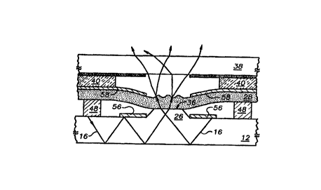
Referring to Fig. 4A there is shown an example mechanical tap ~4~ in
accordance with the invention, in which a ~ombination of elec~rostalic force andmech~nic~l restoring force is employed to move the tap into and out of contact uith the
s light storage plate 12. In an effort to distinguish the various tap components. the figure
is not shown to scale. In this first example design, the flat panel display is assembled
such that each tap in the display is normally '-on " i.e.. each tap is normally cont~cting a
corresponding mesa on the light storage plate.
As shown in the figure the mechanical tap is embodied as a beam 28 and for
20 dual electrostatic/mechanical actuation schemes the beam is preferablv formed of a
material characterized by an internal stress such as a co~ es~ive or tensile stress.
Silicon (Si), silicon dioxide (sio2) or other oxides. silicon nitride (Si(~ l ~N,~3, plastics~
polymers, foils. or other suitable materials can be employed as the mechanical tap beam.
The beam m~t~.n~l iS preferably characterized by a refractive index equal to or greater
25 than that of the light storage plate 12 and is characterized by a reasonable level of
transparency over a prop~g~ting ~li.ct~nce of tens of microns for wavelengths of interest.
As mentioned previously. the tap surface 32 on a side of the tap opposite the top surface
34 of the storage plate mesa 26 preferably exhibits a geometr~ for forward-scattering
light that impinges that surface 34.
CA 02241823 1998-06-29
W O 97/31288 PCT~US97/00369
Based on a consideration of an 'off" state eap distance from the light Slorage
plate in the range of between about 0.5 ,um and 1.0 ~m. example geometric ranges will
be discussed for the tap configuration. It muse be realized. howe~er. that these are
provided as example oniy and that other tap geometries are contemplated by the
s invention. In this example case. the tensile tap bearn 28. of about 0.1 tO 1~lm in
thickness, is fixed to a transparent viewing substrate 38 opposite the light storage plate
by ~ull~ 40. formed of, e.g., silicon dioxide or other material. which is preferably an
in.~lk~tinE~ m~teri~ql. The suppores can additionally be coated with a protective material,
preferably insulating, such as silicon nitride (not shown) for fabrication flexibility, as
0 discussed below.
The viewin~ substrate. in addition to enabling a customizable display v iewing
su}face~ also protects the tap 28 from the ambient environment. The ~iewing substr~t~P
can be formed of, e.g., plastics. quartz. or other clear glass. or other suitable mzlteri~l
Preferably, the viewing substrate robustly withstands fabrication environmentc exhibits
s a degree of thermal expansion comparable to that of the storage plate. and exhibits good
tran~ cy for a prop~g~ti~n ~1iet~n~e of at least about 1 cm. For example. qu~rtz is a
suitable viewing substrate material for silicon nitride tap beams and plastic is a suitable
viewing substrate m~teri~l for plastic tap beams. The lower surface of the viewing
substrate 38 is coated with a dark optical-absorbing layer 42 that suppresses back-
20 reflection of light from the viewing volume. as well as stray light within the viewingsubstrate, from the storage plate. and from the micromechanical tap elements. by
absorbing that light. A window 43 in the optical absorbing layer 4~ is aligned with the
lateral position of the light emittinE surface 32 of the mechanical tap beam 28.The opeical absorbing layer 42 consists of. e.g.. a con~ ctinE metal layer or a
2s metal co~tin~ such as a titaniurn/plz~tinnm layer of about 0.3 ~Lm in thickness.
~lt~rn~tively an optical coating such as CrO can be employed. In the case of a metal
absolption laver. the layer can be pz7tternP~ to form line electrodes for ~ct~l~tin~ the
mech~nic~l tap in accordance with an actuation control scheme described below. In the
case of a non-conducting absorption layer 40. line electrodes 44 are iocated on the lower
CA 02241823 1998-06-29
W O 97/31288 PCT~US97/00369
16
side of the absorption layer. Like the absorption layer. such electrodes consist of ~ e.g.,
about a 0.3 ~m-thick titanium/platinum layer. or other suitable conducting material.
One or more viewing substrate stand-offs 46 are preferably located on the lower
side of the line electrodes 44 to space the tap beam 2~ from the electrodes when the
s beam flexes toward the electrodes. as explained below. The viewing substrate stand-
offs 46 are formed of, e.g.. silicon dioxide. silicon nitride. a plastic. a polyrner. a glass.
metal, or other suitable material. and preferably are of a thickness in the range of
hundreds of angskoms. Even with such small height. the stand-offs act to suppress
contact forces such as Van der Waals 'stiction forces that could develop between the
o relatively smooth upper tap beam surface outside of the scatter region and the line
electrodes 44 if the two surfaces were intimately conr~.~terl The viewing substrate
stand-offs prevent extended intim~Te contact of the surfaces to thereby reduce the
likelihood that strong ;'stiction" forces develop.
Column electrodes 47 are provided on the tap beam 28 on a side opposite that of
the viewing substrate stand offs 46 and line electrodes 44. The column electrodes are
also suitably formed of, e.g., about a 0.3 llm-thick titanium/platinum layer. or other
suitable con~ rtinp material.
In the normally 'ont' light tap con~;guration as illustrated. the light storage plate
~2 includes spacers 48, formed of. e.g., silicon dioxide or other material such as those
20 given above for the stand-offs. that preferably are of a thickness less than the height of
the storage plate mesa 26. For example. for a storage plate mesa of about 10 um in
height, spacers 48 are suitably no more than about 8 ~m in height. Preferably. the
underside 50 of the spacers 48 are coated with a reflective layer so that light impinging
an internal surface of the storage plate 12 at the location of the spacers is reflected back
25 into the storage plate; for some spacer materials the condition of total intemal reflection
may not be met at the storage plate-spacer interface. A coating of. e.g.. silver. of about
lûO nm in thickness is suitable as such a reflecting laver. The sidewalls 5 ~ of the
storage plate mesa are also preferably coated with a reflective layer. Here the reflective
layers are employed to ensure that light escapes only through the top surface 34 of the
30 mesa; such li~ht is scattered by the upper surface 32 of the beam within a range of
CA 02241823 1998-06-29
W O 97/31288 PCT~US97/00369
17
angles that results in a reasonable viewin~ volume relativel~ perpendicular to the
viewing substrate 38.
The display is assembled in the norrnally 'on" condition by pressing the light
storage plate 12 together with the viewing substrate 38: details of this procedure are
s discussed below. Tntim~te contact of the storage plate with the tap beam causes the tap
beam 28. which is preferably tensile. to bend and make positive contact with the top
surface 34 of the mesa 26 because the mesa is of a higher topology than the storage plate
spacers 48. When light 16 is injected in the storage plate 12. it can escape conditions of
total in~ernal reflection at the location of the mesa 26~ where the light is coupled into the
10 contacted tap beam 28 and propagates through it. Upon reaching the back surface 32 of
the tap the light is forward-scattered in the direction of the viewin_ substrate. The
sc~ttered light then couples with the viewing substrate 38. though which it propagates
and emerges into a viewing volurne.
Referring now also to Fig. 4B, this "on" state is nf g~ted by way of electrostatic
15 actuation. Application of an ~ ;ate potential difference between the line electrodes
44 and the column electrodes 47 induces attractive electric charge configurations (not
shown) on the electrodes. resulting in positive attraction of the flexible tap beam 28 and
column electrodes 47 to the fixed viewing substrate and line electrodes 44. Thispositive attraction affec~s a flexing upward of the tap beam. whereby the tap beam
20 moves into contact with the viewing substrate stand-offs 46.
In tnis arrangement. a gap, G. is introduced between the lower surface 32 of thetap beam 2g and the upper surface 34 of storage plate mesa 26. The gap is preferably of
at least, e.g., between about 0.5 ~lm and 1.0 !lm such that light in the storage plate is
n~El;~ihlv evanescently coupled into the tap beam 28. As explained in detail below,
2s once the tap beam 28 moves into contact with the stand-offs 46 on the viewingsll~str~t~. the voltage re~uired between the line and column electrodes to m~int~in this
tap beam position is less than that required to actuate the tap beam; this is due to the fact
that the eiectrostatic force between the electrodes increases greatly as the gap between
the electrodes is reduced.
CA 0224l823 l998-06-29
W O 97/31288 PCTAUS97/00369
18
Actuation of the tap beam ~8 to again "turn on ' the tap is achieved by wav of the
m~rh~nical restoring force inherent in the tensile state of the beam. Removal of the
attractive potential condition between the column and line electrodes allows the tap
beam IO "snap'' back to its resting position in contact with the top surface 34 of the
storage plate mesa 26. Having moved back into contact w ith the mesa. the tap beam
again couples light out of the storage plate and through the viewing substrate 38 into the
viewing volume. This combination electrostatic-mechanical actuation scheme provides
a bistable switch response that facilitates column and line control of a matrix of
m~rll~nical taps. as explained below.
lo Illustrated in Fig. 4B are tap beam stand-offs 54. formed of~ e.g., the tap beam
material. that hold the iower surface 36 of the tap beam 28 v ery slightly out of intim~te
contact with the top surface 34 of the mesa 26 when the tap beam moves to close the
gap between the tap bearn and the mesa. The stand-offs are preferablv of a very small
height, e.g., about 200~. Even with such small height, the stand-offs act to suppress
15 contact forces such as Van der Waals "stiction" forces that could develop between the
relatively smooth lower tap beam surface 36 and upper mesa surface 34 if the twosurfaces were intim~tely contacted across their entire extent. A matrix of tap beam
stand-offs distributed across the lower tap beam surface preven~s extended intim~tf-
contact of the surfaces to therebv reduce the likelihood that strong stiction'' forces
20 develop. The stand-offs are preferably of such a small height. howe~er. that they do not
substantially impact the efficiency of light coupling between the mesa top surface and
the tap bearn lower surface when the two surfaces are brought together. Thus. the tap
beam is said to be "in contact" with the light storage plate when itis in a position that
enables coupling of light out of the light storage plate even though the beam and light
25 storage plate may be slightly separated by the stand-offs.
Referring now to Figs. 4C-4D. a second example mechanical light tap actuation
scheme provides a norrnally "of~' light tap configuration. Here. the light storage plate
mesa 26 is of a height less than that of spacers 48 on the light storage plate 12. Adjacent
to the spacers 48 are line electrodes 56. Corresponding column electrodes 58 are30 located on the upper surface of the mechanical tap beam 2 8. The mechanical tap beam,
CA 02241823 1998-06-29
W O 97/31288 PCT~US97/00369
19
spacers, and electrodes can here be forrned of the same materials described above in
connection with the norrnally '~on" light tap configuration.
In the normally "off" configuration, the tensile nature of the mechanical tap
bearn m~in~;n~ the bearn spaced apart from the upper surface 36 of the storage plate
mesa 26 due to the increased height of the spacers 48 above the mesa. A gap, G. of
about, e.g., 0.7 ~m between the tap beam and the tOp surface 36 of the mesa disallows
coupling of light from the storage plate to the tap beam and upper viewing substrate 38
whereby negligible storage plate light is viewed in the vicinity of the mesa.
Application of an ~lu~liate potential difference between the line electrodes 56
o and the column electrodes 58 induces attractive electric charge configurations (not
shown) on the electrodes, resulting in positive attraction of the flexible tap bearn 28 to
the light storage plate and line electrodes 56. This positive attraction affects a flexing
downward of the tap beam. whereby the tap beam moves into contact with the top
surface 36 of the s~orage plate mesa 26.
As shown in Fig. 4D. this contact "turns on" the me-~h~nic~l light tap. whereby
light is coupled out of the light storage plate mesa through the contacting mechanical tap
beam, and from there through the viewing substrate 3 8 into a viewing volume ~om a
poin2 corresponding laterally to the location of the mesa. Upon removal of the attractive
electrode potentials. the tensile mechanical tap beam snaps upward to return to its
norrnal resting position in which a gap, G, separates the tap beam from the top surface
of the light storage plate mesa. Hence. in contrast to the normally "on configuration,
the display e}ement here requires application of a potential to initiate viewing of light.
In yet another exarnple of a mechanical light tap configuration. as shown in Fig.
4E, the height of the light storage plate mesa 26 is here less than that of spacers 48
separating the mechanical tap beam and the light storage plate 12. Electrodes 60, 62, 64
are provided on the viewing substrate 38, upper surface of the tap beam 28. and the light
storage plate 12. respectively. for actuating the tap beam in a tri-electrode scenario. In
this case the light tap is m~int~inecl out of contact with the light storage plate at an
intermediate point. e.g.. half-way. between the light storage plate mesa and the viewing
30 ~ul,~l,dte, when the potential difference between the mechanical tap beam and the light
CA 02241823 1998-06-29
W O 97/31288 PCTAUS97/00369
storage plate is about the sarne as the potential difference between the mechanical tap
bearn and the viewing substrate.
Application of an ~pp,-~pliate voltage between the tap bearn electrodes 62 and
the light storage plate electrodes 64 results in deflection of the tap beam toward the
5 upper surface of the mesa 26 and contact of that surface, whereby light is coupled out of
the light storage plate and into a viewing volume of the viewin~ substrate 38. Acombination of mechanical and electrostatic forces can then be employed to draw the
tap beam upward and out of contact with the mesa by way of application of an
a~plo~,l,ate voltage between the viewing substrate electrodes 60 and the tap bearn
lo electro~es 6~. In this three-electrode configuration. electrostatic force alone can be
employed for actuating the mechanical tap beam: that is. a mechanical restorin~ force
provided by, e.g.. a lensile internal stress condition of the tap beam is not needed.
Tn~te~-l electrostatic attractive force alone can be employed for moving the tap bearn in
either direction.
Many variations ofthe merh~nical tap beam actuation sch~ s described above
are co~ lated by the invention. For example. as shown in Fig. 5~ an electret
configuration can be employed for producing electrostatic actuation. EIere a layer of
excess charge 66 is embedded in the upper surface of the li~ht storage plate. Asexplained in detail below. such a charge layer can be produced by~ e.g.. ion-implamation
20 of a light storage plate material such as a transparent form of teflon or an oxide such as
silicon dioxide. In, e.g., a normally "on" geometry. the embedded electrel produces
corresponding attractive image charge in the tap beam electrode 47~ resulting in a
colls~ electrostatic downward force on the tap beam. holding the beam in contact with
the top surface 34 of the light storage plate mesa 26. This force is relatively
2s independent of the gap between the electret 66 and the beam electrode 47 Placement of
a sufficiently large potential difference between the tap beam electrodes 47 and the
viewing substrate electrodes 44 counteracts this static force and causes the tap bearn to
fiex upward a~ainst the viewin~ substrate stand-offs 46. thereby "turning off" the
display tap. as sho~n in the fi~ure. Upon removal of the potential difference, the
CA 0224l823 l998-06-29
W O 97/31288 PCT~US97/00369
attractive electret force again causes deflection of the tap beam aownt~ ard and into
contact with the storage plate mesa.
The static, attractive electret force generation mech~ni~m thereby presents itself
as an ~It~rn~ive to the mechanical force generation mec~h~ni~m of the static tensile tap
5 beam condition described above. Both schemes provide a bistable actuation scenario7
but do so with <lirr~ static force generation schemes. Thus. a configuration including
an electret can employ a tap beam material that is not necessarilv under tensile stress.
Polystyrene and silicon nitride with low tensile stress are examples of suitable m~t~
As will be understood by those skilled in the art, each scheme has specific advantages
10 that may render that scheme superior for various applications. For example~ because the
turr~-on and turn-off forces of the electret confi~uration are proportional to the
embedded charge density, q-, and are independent of the internal stress. T~ of the
m~rh~nical tap beam. the electret scheme is not constrained to specific tap material
conditions and accordingly, a wider range of materials can be considered for the electret
15 sch~me
Con~iclPrin~ other variations of the tap actuation scheme. the mechanical tap
beam can be actll~tf!d based on a static internal compressive~ rather than lensile~ stress
condition. In this case the tap beam exhibits a constant tendency to bow out of plane.
As will be understood based on the previous discussion of actuation of a tensile beam,
20 such a co.~ ,si~e beam could be configured in either a normallv ~ on or normally
"o~' scheme depending on the relative heights of the light storage plate mesa and the
spacers sepa~ lg the mechanical tap beam from the light storage plate and the viewing
~U~ Ldl.C. Electrode configurations can be employed on the tap beam. viewing
substrate, and/or light storage plate to produce a desired electrostatic force generation
25 mech~ni~m in concert with the mechanical restoring force produced by the colll~lcs~ e
tap bearn condition.
For any of the various actuation schemes contemplated bv the invention, light
trapped in the light storage plate can be released and viewed through the light storage
plate itself~ the mechanical light tap beam~ a transparent viewing substrate adjacent the
30 m~ch~nical light tap beam. or other suitable viewing surface. In a configuration in
CA 02241823 1998-06-29
W O 97/31288 PCTrUS97/00369
which a transparent viewing substrate is employed. it is preferable that the upper surface
of the mechanical tap beam and the surface of the viewing substrate adjacent them~cch~ni~s~l tap beam be processed to optimize both coupling of light between the tap
bearn and the viewing substrate and scattering of light into a reasonably wide vie~,ving
5 angle through the viewing substrate.
In the configurations described above (Figs. 4-5). the lower surface 43 of the
viewing substrate 38 is smooth and flat. Alternatively~ as shown in Fig. 6A. the region
70 of the viewing substrate that laterally corresponds to the location of the roughened
region 32 of the beam 28 can also include geometric asperities. Witn this configuration,
o both the upper surface 32 of the mechanical tap and the lower surface 70 of the viewing
substrate can provide a geomerric optical scattering surface: this increases the spreading
angle of the emitted light. In any of the these cases. it is preferable that the optical
scdllc;~ g surface be optimized for Lambertian scattering properties.
Without an effective scattering mech~ni~m~ light coupled through the
15 mçr,h~nical tap and imo a viewing volume may likely enter the viewing volurne at
angles quite obtuse from a direction perpendicular to the display. In other words. Iight
exiting the display may likely be directed outward at angles close to the display surface
if it is not first scattered. w hereby a viewer could see the exiting light only at locations
away from a direction perpendicular to the display. But as a practical matter. the most
20 ~ulcf~l~c,d position for viewing a display is indeed typicallv centered around a direction
perpendicuiar to rhe display surface. and accordingly, only about 2 steradian of light
within the vertical (and horizontal) angular spread of light emitted into a viewing
volume is useful.
In the invention. a scatter mech~ni~m~ and preferab~y one that achieves
2s Larnbertian scattering. ensures that the arc of viewing angles of light exiting the display
is generally around a direction perpendicular to the display surface at the location of the
point at which light e~:its the display surface. A wide range of scattering me~h~ni~m~ is
contemplated by the invention. Beyond roughening of the tap beam and/or viewing
~ub~LldLe surface. any surface perturbation. e.g., a periodic or aperiodic grating~ faceted
30 pattern, or other geometric perturbation. can be employed as a scattering mech~ni~m
CA 02241823 1998-06-29
W O 97/31288 PCT~US97/00369
~1tern~tively, a surface coating or other layer that provides scattering functionalitv can
be ~ocated on the tap beam and the viewing substrale surfaces. In yet another
~l~rn~tive~ a separate scattering medium such as a scatter beam element can be
positioned atop the tap beam. The tap beam can alternatively be itself formed of a
5 material that facilitates scattering; for exarnple~ the tap beam can be formed of a
tr~n~1uc~nt material. As will be recognized by those skilled in the art. other sc~l t. ~
m~rh~ni.~m~ are also suitable. A specific scatter mechanism or medium is not re~uired
by the invention, rather, it is the ability to effectively scatter light in the light tap beam
that is preferably provided by a selected meçh~ni~m
IO Considering yet another alternative of the mechanical tap configuration, as
shown in Fig. 6B~ the viewing substrate can include a color layer 68 located in a lateral
position that col~ olIds to the location of the light storage plate mesa. Suitable dyes
that filter, e.g.~ red. green. or blue wavelength components of white light trapped in and
released from the light s~orage plate are here impregnated in the lower surface of the
viewing substrate. In an ~1t~rn~tive scheme, the color layer 68 includes one or more
I11minPscent materials that each emit a selected color or colors when the lnminescPnt
mzltf~ri~Tis excited by ultraviolet light trapped in and released from the light storage
plate. Exarnples of suitable 111minescent materials are described in Luminescence of
Solids, by H.W. Lewrenz. Dover~ 1968.
The invention is not limited to the variations in actuation mech~ni.~m~ or
m~rhzlnical tap configurations described above. Rather. the invention contemplates any
m~r.h~nic~l tap scheme that suitably provides the ability to actuate a merh~n;~1 tap for
making contact to a light storage plate to release light from the plate into distinct
viewing locations. Preferably. the actuation mech~ni~m achieves a stable merh~ni~1
2s response to the actuation force that exhibits, e.g.~ bistability. Cantilever bearns, bearns
~u~vlLed by two or more 7Uy~ol i~, plates. diaphragms. and other such mech~nic~1structures are examples of alternative tap conf1gurations cO~ ed by the invention.
~teri~1s under co,l,~res~ive stress, rather than tensile stress~ or under no internal stress,
are also suitable with corresponding actuation schemes.
CA 02241823 1998-06-29
W O 97/31288 PCT~S97/00369
24
Whatever geometrsy the tap element takes. it can itself provide a raised contactsurface such as a mesa in addition to or instead of that provided by the li~ht storage
plate. In one such configuration, the light storage plate is smooth and each tap element
includes a mesa protrusion on its lower surface for contacting the light storage plate.
The height of the mesa is selected to produce a desired assembly configuration for a
norrnally on or normally off actuation scheme Alternatively. but not preferably for
many cases. neither the tap element nor the li~ht storage plate may provide a raised
contact surface.
Of the example actuation me~h~nicm~ discussed above. those emp}oying a
lo combination of electrostatic and mechanical restoring forces provide bistability, which
ma~ be preferable for some applications. The force required to turn on' the mechanical
tap in the case of a norrnally "off'' configuration (Figs. 4C-4D) and the force required to
"turn off~' the mechanical tap in the case of a normally "on confi~uration (Figs. 4A-4B)
is proportional to the voltage applied between the mechanical tap beam electrode and
IS either the light storage plate electrode or the viewing substrate electrode for producing a
potential difference between those e}ectrodes. and the extent of the gap between the
mechanical tap bearn and the respective electrode toward which the tap bearn is being
~Ct~ tt~1 This electrostatic force, ~ is ~iven as:
F,~ ~f~,,~2)WLfl~/fx T d/~r))-. (.
20 where ~7 is the free-space dielectric constant~ u~ is the width of the mechanical tap beam,
L is the length of the mechanical tap beam suspension between the supports, V is the
voltage applied between the tap beam and the other ~lCt~tin~ electrode, x is the gap
between the mPt h~nical tap beam and the ~t-l~tin~ electrode. d is the thickness of the
tap beam. and ~r is the relative dielectric constant of the tap beam.
The trans~erse mechanical restorin~ force, F",. that inherently acts to actuate the
mechanical tap beam in the opposite direction is given by:
T(wd/L)y (6)
where T is the internal tensile stress of the tap beam~ and ~ is the displacement of the tap
beam from its restin~ (taut) position.
CA 02241823 1998-06-29
W O 97/31288 PCTrUS97/00369
To effecti~ ely move the mechanical tap beam through the total gap distance G inopposition to the inherem mechanical restorin~ force. the electrostatic force must be
produced by a voltage, 1. of sufficien~ magnitude to overcome the merh~nic~l restoring
force. Given that such a voltage is employed. expressions (5) and (6) above provide an
5 indication of the force to which the mechanical tap beam must subjec~ed to switch
bet~,veenthe -'on" conditionand off' condition.
Expressions for estim~tin~ the switching time are highly nonlinear. and a
nurnerical technique is used to solve for conver~ent switching time value. One
approach for estim~ring the closure switching time of the mechanical elements shown in
10 Figs. 4C and 4D is as follows. Given that an increment of distance throu_h which a tap
bearn moves is D = G/N~ where C~ is the extent of the tap beam gap and .~\ is a large
number, e.g.. greater than 10. and given that n = I . 3.. i- 1.. ~-1. N: then. for the ith
increment. x, = G - i x D and yi = i x D. Then expression for time duration is given as:
at = (v, ' ) + 2D ~ , (7)
with aj = (Fe(xJ + F",(yJ)/pwhd. and ~~, = v, / T aj~t~ .
where p is Ihe density of the mechanical tap beam material. The time required to close a
tap beam switch is then given as:
t = ~ ". (8)
"=~
Considering the actuation speed of an example mechanical tap beam configuration in
20 which the tap beam is formed of highly-stressed silicon nitride. e.g., as a LPCVD layer
of nitride, e~pressions (73 and (83 above in~iic~te that the electrostatically-~ct-~tecl
closing of the tap beam relative to the light slorage plate is achieved in about 230
nanoseconds. A similar computalion can be made to estim~t~ the time needed to open
the tap beam switch shown in Figs. 4C and 4D by substituting for expressions Yi and a"
2s in ~ essions (7) and (8) above, ~, ' = G - i ~; D. and a; = ~f;m(yl ')/p w~ d. respectively.
In this case. the applied voltage. T: is set to zero. because the mechanical restoring force
alone provides the tap beam actuation. These substitutions provide an estimation that
CA 02241823 1998-06-29
W O 97131288 PCTrUS97100369
the m~ch~nically-aclualed opening of the tap beam is achieved in about ''~0
nanoseconds.
The closing and opening switch time computations assume a silicon nitride
stress condition T. of about l x l O9 N/m . a silicon nitride densih . p. of about 2700
S Kg/m3, a dielectric tap beam thickness. d~ of about 0.1 ,um and dielectric constant, ~r~ of
about 8., a tap beam suspension length, L. of about 180 ~m. a gap. G. of about 0.7 ~lm,
and an electrostatic actuation voltage. ~. of about '~S volts during Ihe actualion time.
The computation does not explicitly take into account stiffness and curvature of the
m~chRnical tap beam as the beam flexes. e.g.. against the top surface of the light storage
o plate mesa: does not explicitlv take into account pneumatic forces. the mass of the
electrodes on the tap beam. or the mass of a light-scattering medium. Ia~ er. or surface on
the tap beam. Even withoul such considerations. however. the sub-microsecond speed
indicated by the computation pomts out that a very high-speed display can be realized
using a matrix of such mechanical tap beam elements. as ~ cucsecl in detail below.
The actuation response of the merh~nical tap beam to a combination
electrostaticimechanical actuation scheme is bistable. as men~ioned above. and this
bistability, in combinalion with the proximity effect inherent in electroslatlc actuation,
results in a predictable actuation hvsterisis function. Figure 7 illustrates this actuation
hysterisis function for the example case of Figs. 4C-4D in which the mechanical light
20 tap is configured in a normally ' off" scheme. The dynamic distance between the
mtorh~nical tap beam and the top surface of the light storage plate mesa is given as x,
where x is equal to G. the full extent of the gap. when the tap is fully open. The
potential dirr~,e~lce applied between the mechanical tap electrodes and the light storage
plate electrodes is given as 1'~ where V can be a positive or negati~e voltage: due to the
25 polarity-independent attractive charge formation mechanism inherent in electrostatic
actuation. the applied voltage can be of either a positive or negative polarity.When the applied potential difference~ l~r. is zero~ the lension in the mechanicai
tap beam m~int~in.c the beam in the "open ' position~ where r = G. indicated by point
"A'' in Fig. 7. The mechanical tap beam continues to m~int~in this position when a
30 positive polaritv potential difference is applied~ until the applied potential difference
CA 02241823 1998-06-29
W O 97/31288 PCTAUS97/00369
exceeds a threshold voltage, T ",. defined as that volta~e which produces an eiectrostatic
force equal to the inherent mechanical restoring force of the tap beam. At applied
potential dir~ellces greater than Y", the mechanical tap beam experiences a larger
eleclrostatic force than mechanical restoring force and tends to move toward the ligh~
s storage plate. indicated bv point "B" in the figure.
Once a potential difference equal to or greater than a closure voltage, T~c~ is
applied the tap beam experiences an electrostatic force adequate for ~c~ ing the beam
completely through the gap, G. whereby the tap is in the 'closed' position. in~ic~ted by
point "C" in the figure, and for which light is coupled out of the light storage plate and
10 into a viewing vo}ume. The magnitude of the applied potential difference does not
thereafter need to be increased beyond than the closure voltage m~gnilllcZe because the
closure voltage magnitude is sufficient for moving the tap beam completely across the
gap G.
Based on the expression for electrostatic force~ Fe~ given above in ~xl~ci,sion (5),
IS it is understood that as the tap beam moves closer to the actuating electrode~ the tap
beam experiences a stronger electrostatic force; this is reflected in the inverse
relationship between F~ and x in expression (5). Once the tap bearn is separated from
the light storage plate mesa onlv by the verv tin~ stand-offs on the lower surface of the
tap beam (54 in Fig. 4B)~ the electrostatic force is quite strong due to the proximity
20 effect~ which embodies the inverse relationship between electrostatic force and distance.
As a result. the tap beam remains in the ' closed' position even when the applied voltage
m~gnit~1cle is decreased below the closure voltage~ l~c This fortuitous condition enables
a display scheme in which the applied voltage required to hold a given tap beam closed
is much less than the voltage required to first close the beam. and results in a reduced
25 power requirement over typical display schemes. as discussed below.
Once the applied potential difference magnitude is decreased below the
threshold voltage. T ,". corresponding to an electrostatic force equal to the merh~nical
restoring force of the mechanical tap beam. and is decreased further to a closure voltage
threshold, VD. the mechanical restoring force again dominates the electrostatic force, and
30 the tap beam moves back toward the open position. as indicated by point "D" in Fig.
CA 02241823 1998-06-29
W O 97/31288 PCT~US97/00369
7. Thereafter. any applied potential difference ma~nilude equal to or }ess than an open
voltage, I'o7 results in ' snapping" of the tap beam back to its rest position away from the
light storage p}ate mesa. as indicated by point 'E'' in Fig. 7.
With this acluation response. the mechanica} tap beam is seen to exhibit a
5 bistable hysterisis response of either ' open" or ''closed' conditions~ wherein I ! an
applied potential difference magnitude of at least F c closes the tap and holds the tap
closed; 2) an applied potential difference magnitude of less than ~O opens the tap and
m~int~in.~ the tap open; 3) an applied potential difference magnitude between ~O and ~c
m~int~in~ the tap in the open position if the tap's most recent actuation was opening;
10 and 4) an applied potential difference magnitude between T ,, and Vc m~inr~in~ the tap in
the closed position if the tap's most recent actuation was closing. This hvsteresis
response is polarity-independem~ as explained above and as is illustrated in Ihe left half
of Fig. 7.
A similar hysteresis actuation response is provided by a three-electrode tap
15 scheme like that shown in Fig. 4E wherein an electrode is provided on all of the tap
beam. the light storage plate. and the viewing substrate. In this case. no mechanical
restoring force is employed; only electrostatic force actuates Ihe tap beam. ~ere, the
force, F", on the tap beam when in the "off" up position. and the force. ~D. on the tap
beam when in the 'on" down position are given as~ respectively:
F oc( b~); (Y+~ ) (9)
where 1i'U is the potential difference between the viewin~ substrate and tap beam
electrodes (60 and 6'~ respectively~ in Fig. 4E)~ I'D is the potential difference between
the tap beam and storage plate electrodes (62 and 64~ respectively~ in Fig. 4E), x is the
gap between the tap beam and viewing substrate electrodes at any given time, and y is
25 the gap between the tap beam and storage plate electrodes at any given time.
In one example 3-electrode actuation scheme~ a constant potential. i~e., DC
voltage, T ," is m~int~ined between the tap beam and viewing substrate and the potential
between the tap beam and storage plate, YD~ is changed. In this case, given that the tap
beam is initialized in the "off" up position~ the tap beam will remain in that position
CA 0224l823 l998-06-29
W O 97/31288 PCTAUS97/00369
29
until the applied voltage between the tap beam and storage plate electrodes produces a
potential difference between those electrodes. r D. that exceeds a closure actuation
voltage, VC Thereafter. ~he tap beam closes and remains in Ihe on down position until
- the applied voltage between the tap beam and storage plate electrodes produces a
5 potential difference between those electrodes that falls below an opening potential
di~rc.cl~ce, T~o~ The closure potential difference~ 1~. and the openino potential
~lir~lcllce, 1~o~ are given as:
V > y ( Ym;lx + ~. ) ( Y --',
Xmjn Xmax
where Ymm- ,Yma~ Xm"?, and x",~,~ are the minimum and maximum separations between the
lo tap beam and the storage plate and viewino substrate. respectivel~. As will be
reco~nized by those skilled in the art. a DC potential might alternatlvek~ be applied
between the tap beam and the light storage plate rathe~ than the ~iewing substrate. In
either case. it may be preferable in some applications to periodically reverse the polarity
of the DC potential and the corresponding actuation potential to suppress elec~ronic
5 charge build up on the tap beam. Such charge build up could result in a strongelectrostatic force that swamps out that produced by the applied volta~es.
A hysteretic actuation response is also achieved by a tap scheme in which. as
shown in Fig. 5, electrodes are provided on the tap beam ana. e.g.. the viewing substrate
and an electret is provided in. e.g.. the lioht storage plaee. Here a~ain no mech~nic~l
20 restoring force is required to actuate the tap beam. In this case. the downward force, FD,
on the tap beam. is a function of the electret charge density. D: and the upward force, ~u,
is a function of the potential difference, 1~" between the tap and viewing substrate
electrodes. These forces are given as. respectively:
FD ~ D2; F ~ ~ r ~
25 where x is the distance between the viewing substrate electrode and the tap beam.
In one example 2-electrode/electret actuation scheme. the potential difference ~u,
between the tap and viewing substrate electrodes is changed to actuate the beam. Given
CA 0224l823 l998-06-29
W O 97/31288 PCT~US97/00369
that the tap beam is initialized in the on" down position. the tap beam will remain in
that position until the applied voltage between the tap beam and viewin_ substrate
electrodes equals or exceeds an opening potential difference. r~,. This causes the tap
beam to move up to the off" position~ where it remains until the potential difference T~" ~
between the tap and viewing substrate electrodes is decreased below a closure potential
difference~ Y~. The closure potential difference. V~. and the opening potential
difference, V0, are given as:
V" 2 D(xmay +~ Y < D(X~nlll + ~ (12)
where Xm,n and xma" are the minimum and maximum separations between the viewing
0 substrate electrodes and the tap beam. As will be understood by those skilled in the art.
other hysteretic actuation schemes can be emplo~ed with a 2-electrode. 3-electrode.
electret, or other electroslatic actuation schel~ie. If bistable. hysteretic response is not
required~ a wide range of electrostatic acauation control techniques can ailernallvely be
employed. The electromechanical optical switch of the invention does not re~uire a
specific control scheme~ but instead contemplates a wide range of control schemes that
employ electrostatic force at least in part for actuation of a mechanical tap structure.
Considering now in more detail a flat panel display employing an array o~
me~,hzlnical light taps provided b,v the invention as pixel elements. as sho~vn in Figs. 8A,
8B. and 8C. the displav 10 ConSisEs of a light storage plate 1 havinQ light sources 14.
which preferably are white light or multi-color light sources. on each lateral end of the
storage plate. The light storage plate forms the back of the display, opposite the viewing
side; which consists of the viewing substrate 38~ as described above. A display area 72
is defined by the area on the viewing substrate that corresponds to an array 76 of
m~ch~nical tap beam structures aligned in columns. examples of ~hich were shown in
Fig. 4. The viewing substrate 38 and light storage plate 12 are aligned and held together
preferably under a partial v acuum. An O-ring 78. deposited on the viewing ~ul~LlaLe 38,
facilitates this evacuated assembly.
Line driver electronics 80 and column driver electronics 82 are positioned at the
top and bottom edges of the viewing substrate 38. In one suitable example
configuration. dedicated line drivers 80 are each connected to a corresponding line
CA 02241823 1998-06-29
W O 97/31288 PCT~US97/00369
electrode on the viewing substrate by wav of line conductors 81: and similarly.
dedicated coiumn drivers 82 are each connected to a correspondin~ column electrode on
a mechanical tap beam bv way of column conductors 83.
An example flat panel display ~n accordance with the invention is of a geometry
5 in which the active display area (76 in Fig. 8C) is about I meter-wide and has a height
of about 56 cm. The display provides~ e.g.~ 1080 display lines. with 1920 pixei elements
per line. Pixel intensity modulation. e.g.~ ei~ht-bit modulation. is optionally provided by
a t~ L,oldl- or area-weighting scheme. described below. With these geometric
considerations. the example display suppor~s a frame rate of 60 frames/sec. aiso0 optionally supporting multi-color sub-frames. e.g.. 3 color sub-frames/frame. High
optical efficienc~. of the sub-frame scheme is achieved if. e.g.. red. green. and blue light
sources are pulsed in sequence to illllmin~r~ the light storage plate in a sequence of red.
green~ and blue sub-frame color time slots. In such a scenario. each of the three color
time slots is 113 of the total frame duration provided by a frarne rate of 60 frames/sec.
and accordingly corresponds to about 5.56 msec fior each color time slot. The ~t~nl~hon
time of the array of mechanical light taps. given above as in the range of hundreds of
nanoseconds. provides adequate speed for such a multi-color scheme. as explained in
more de~ail belour
In a controi scheme for setting the -on and 'off' states of the pixel arrav for one
~o color time slot or in a case in which sequential color injection is not used. for one frame.
voltages are applied to the line and column electrodes of the display to electrostatically
actuate selected mechanical tap beams in the array. In one example control scheme. as
shown in Fig. 9:
VcO,i = Voltage applied to i'h column electrode where i= I to m:
V~ne~ = Voltage applied tO jth line electrode wherej = 1 to n; and
Vd~ 'coli - Vlinej) = Differential potential applied to the mech~nic~l
tap located at the intersection of the ith column electrode and the j'h line
- electrode.
In one exarnple of this control scheme. all of the column electrode voltages areapplied simultaneousl~r~ duringT the application of a gi~ell line electrode voltage: then the
CA 02241823 1998-06-29
W O 97/31288 PCTrUS97/00369
column electrode voltages corresponding to the next sequential line are applied
simultaneously while the next line electrode voltage is applied. The line electrode
voltages are in this way applied sequentially beginnin~g with. e.~ .. the top-most line.
During each line electrode voltage application. the i'l' column voltage, T~cor~ applied to
5 each of the r = 1 to m column electrodes. is either t ~5 or - Vs where 1~5 iS defined as in
Fig. 7, and is " ,~ i, I t5~ il,ed for the duration of a given line electrode actuation period. The
jt~t line voltage, T~nej~ applied to the jt~1 of the j = 1 to n line electrodes~ is + Vs during the
sctuation period for that line. and is 0 volts while all of the other lines are being
addressed.
Electronics for enabling this actuation scheme are described later in the
discussion. Whatever eleclronics are emploved. for many applications it may be
preferable to configure the display such that the line and column actuation voltage Vs~ is
constrained to a magnitude less than abut 20 V such that conventional MOS technology
can be employed. ~or the example ~eometry considered in the above computation of15 switching speeds a line and column actuation voltage, ~s~ of at least about 12.5 V is
required. In this case. one or more of the various geometric parameters can be adjusted
to achieve a desired actuation voltage magnitude. e.g.~ a lower magnitude than 12.5 V.
Considering the example control scenario shown in Fig. 9. which depicts a point
in time during one frame or color time slot when lines I and 2 have been addressed and
20 line 3 is actively bein_ addressed. column electrodes i = l and i = ~ are set at an
example voltage of+l~s and column electrode i = 3 is set at an example voltage of-Vs;
line electrodesj = l and j = ~ are set at 0 volts and line electrodej = 3. the line actively
being addressed. is set at ~ Vs With these column and line electrode voltaszes~ the
mPchzlnical taps addressed at a time previous to that depicted in Fig. 8, i.e.! those taps at
~5 the intersections of all the colurnns and lines l and 2~ all are exposed to a potential
difference of either + I~5 or -1'5. Based on the hysterisis actuation response of the
mechanical tap scheme. as shown in Fig. 7. these voltages set those mech~nical taps at a
point in the hysterisis function whereby the taps remain at whatever position they were
set at when they were each activelv addressed. even though no active addressing of
30 those lines continues. This condition is m~int~ined provided that the transition to or
CA 02241823 1998-06-29
W O 97/31288 PCT~US97/00369
from +Ys or -r'5 occurs in a time inlerval short with respect to the mechanical switching
speed of the elements and is a result of the bistable hysterisis actuation response.
The mechanical laps al the intersections of the active line. Iine 3. and columns i
- and 2 are exposed to a potemial difference of 0 volts. whereb~ these two taps are
5 opened. The mechanical tap at the intersection of column 3 and line 3 is exposed to a
potential difference of + ' 1~5, which is greater than + T'c (Fig. 7). As a result. this
m~r~h~nical tap is closed. and li~ht is coupled out of the tap into the viewing substrate.
At a time after the third line is actively addressed, i.e.. after the voltage applied to line 3
is switched to 0 V~ the - open' and "closed" states of the taps in that line will retain their
10 positions due to the hysterisis actuation response of the taps. In this manner. the emire
sequence of line eiectrodes is addressed with Laps relalnin~ their position while later taps
in the sequence are addressed. This scheme elimin~tes the need for active electronic
devices at each pixel and provides an extremeiy efficient display ~ ith low power
con~l~mption.
Is Furtherrnore, this e}egant control scheme requires onlv three different voltage
m~nihl~les~ namely, -Y5 +Vs~ and 0 volts, and vet the bistable hvsleresis actuation
response of the mechanical tap scheme provides the ability to achieve four different
responses. namel~ "open. ~ close.~ remain open~' and remain closed." As explained
above~ the various column electrode voltages are applied simultaneously and switched
20 simultaneously at the start of each line voltage application~ while the line electrodes are
set sequentially. Alternatively but perhaps less preferablv. the column and lineelectrode actuation voltages and control timing can be switched~ i.e.. +V5 can be applied
to the line electrodes simultaneously and 0 V or + Y5 applied to the column electrodes
sequentially. Whichever electrodes are addressed sequentially. the voltage applied to
2s each electrode in the sequence is preferably applied for a time duration that is sufficient
to est~hli~h an electrostatic actuation force. after which the appropriate voltage is
applied to the next electrode in the sequence. The polarity of the colurnn (or line)
~oltages that are applied simultaneously are set at the start of the actuation time duration
for a given sequential line ~or column) and are switched at the start of the actuation time
30 duration for the next line (or column) in the sequence.
CA 02241823 1998-06-29
WO 97/31288 PCT~US97/00369
34
Considering a quantitative example of the control timing sequence for applying
column and line voltages, recall that the flat panel displav of the invention supports a
temporal scheme in which about ~.56 msec is available for each of three color time slots
in a frarne, where the frame ra~e is 60 framesisec. ~eferring to Fig. 1 OA. each color time
5 slot corresponds to a temporal segment during the frame duration in which either red~
green or blue light is produced in the location of any of the mechanical taps that are set
"on" for that time slot. In one example scenario. one-half of the color time slot duration.
i.e.. about ~.78 msec. is allotted for acluating the mechanical tap beams to move seiected
ones into the "on" condition. and the r~m~ininP time. also ~ 78 msec. is allotted for
fl~hin~ of color li~ht source lamps to produce the desired color of a ~given time slot.
Referring to Fig. 1 OB. the actuate and flash sub-time slots correspondin~ ro each color
time slol are ill~l~traTt-~ For example. the first red" color time slot in Fi~g. lOA, i.e.,
time slot number 1. is produced by a first actuation sub-time slot (Fig. 1 OB) to ''set the
frame" during which all of the line electrodes are sequentially addressed to actuate
1~ selected ones of the mechanical taps into the on' condition. followed by a first "flash"
sub-time slot during which red light is injected into the light storage plate. The
sequence progresses in this manner to produce green and blue time slots in one frarne
duration. Thus~ each mechanical tap in the displa~ may be actuated up to three times ~o
produce one displa~ frame.
In an alternative scheme. a given color source can be m~inl~ined on during an
entire color time slot duration. e.g.~ 6 msec. In this scheme. all tap elements are set
in the "off" position at the start of a given color time slot and are switched to ap~op~late
settings sequentially in a time short with respect to the time slot duration. The elements
are then turned off sequentially prior to the next color time slot.
Actuation schemes like these employ a combination of column electrode and line
electrode voltage application. as explained above. If. e.g.. all column electrodes are to
be addressed simultaneously, then the column driver electronics is controlled to, e.g.,
drive two half-columns of pixels. for example the top-half plane of the display and the
bottom-half plane of the displ.sv. independentl~ and simultaneously. This dual column
30 actuation enables the addressing of two line electrodes. Then. if the line electrodes are
CA 02241823 1998-06-29
W O 97131288 PCTrUS97/00369
to be addressed sequentially. the time available to address a single line is e~ual to the
actuation time slot duration divided bv one-half the number of lines in Ihe display. In
one sequentiai addressing scheme in accordance ~vith the invention. Iine driver
- electronics are controlled to sequentially address lines beginning at the top of the display
5 while simultaneously addressing lines begim1in 1 at the bottom o~ the display. In this
scheme, e.g.? lines l to nl2 (where n is the number of lines) are addressed in sequence
while lines n to (nt2)+1 are simultaneously addressed in sequence. This scheme
accompl;ch~ addressing of all lines with twice the time available than would be
available if all n lines were addressed in sequence from line 1 to line n.
lo With this line addressing scheme. the time allotted to address one line is 2.78
msec/(1080/21 = 5.15 ~Lsec. for a display includin~ 1080 lines. Fi~. lOC schematically
depicls this sequemial addressing scheme for the top half of the displa- . cont~in;np line
I to line n/2. The actuation voltage - I, is sequentially applied to each line for a ume
cc~l.c~ollding to the address line time. e.g.? ~ usec. as computed above. This address
1~ line time is more than sufficient to accommodate both the frame speed and switching
speed of source lamps as well as the mechanical actuation speed of the merh~ni~-~l light
taps. Indeed. this illustrates an important advantage of the mech~nic~1 light tap scheme
relative IO more convemional displav schemes that ~ypically are either much slower or
that re~uire a more complicated actuation con~;guration.
As explained above. each micromechanical element in the flat panel display
corresponds generally to the intersection of a column electrode and a line electrode.
because an electrostatic force generated at such an intersection results in actuation of a
mtor~ nical tap beam to contact the light stora~e plate at the location of the intersection.
Thus, at the location of every column and lh1e electrode intersection in the light tap
array there is located a corresponding contact area~ which may include topology such as
a mesa on, e.g.~ the light storage plate. As explained previously? a mesa or other contact
topology could alternatively be located on the li~ht tap elements themselves. The
contact topology. in concert with the compact nature of the li~ht tap eiements and
localized actuation enabled b- the column and line electrode geometry. enables a display
with superior resolution.
CA 02241823 1998-06-29
W O 97/31288 PCTrUS97/00369
36
In one example pixel geometr,v in accordance with the invention, as shown in
Fig. 117 an area-weighting scheme is emplo~ ed such that. e.~.. eight bits of viewing
intensity are associated with a single pixel. Other pixel wei~hting schemes are equally
applicable. as described belo~-. The view in Fi~n 1 1 is from the back of the display with
5 the light storage plate removed such that the bottom surfaces of the mechanical tap
bearns are in vlew (as in Fig. 8C) above the lower surfàce of the viewing substrate. As
shown in Fig. I l. one pixel 75 is defined b,v the area of intersection of eight mechanical
tap beam elements 28a-28h. and one line electrode 44 (with reference to Figs. 4A-4D).
The line electrode 44 is located on the lower side of the viewing substrate and extends
lo the horizontal length of the active display area: a displav oi: e.g.. 1080 lines includes
1080 such horizontal electrodes. Each of the ei_ht tap beam eiemems is aclually a
portion of a beam that extends the ful} height of the active display area: a display of e.g,,
1920 pixels/line therefore includes 1920 x 8 = 15.360 such mechanical tap bearns. Each
of these beams corresponds to a column electrode. e.g.. a metzlili7~-1 top surface of the
beam, to which a voltage of either + Vi is applied. as explained above. during addressing
of each line.
In one example voltage control scheme f~r simultaneouslv addressing all 15.360
tap beam columns. an upper set of 15,360 column drivers is provided at the top of the
display and a lower set of l 5 .3 60 column dri ~ ers is provided at the bottom of the
zo display. Preferably. as discussed in more de~ail below. each of the drivers is a fast-
acting double-pole. double-throw switch that applies either iYs to the corresponding
pixel tap bit beam. As is readilv understood. the number of column drivers corresponds
to the nurnDer of bils per pixel; and suitable division of pixel addressing belween
electronics at the top and bottom of the displ:~y can take manv configurations other than
that specifically described here.
Turning again to Fig. 11. in one suitable pi~el design. one pixel extends about
~OQxSOû llm~. with a horizontal border 76 and a vertical border 78 laterally enclosing
the eight taps and verticallv enclosing a section of the eight taps that corresponds to the
horizontal location of a given line electrode. In one example design. each of the eight
mechanical taps is about 40 llm-wide. 180 ~m-long. with two storage plate contact areas
CA 02241823 1998-06-29
W O 97/31288 PCTAUS97/00369
between the supports 40 at each end of the line electrode ~ and a support 40 in the
center of the tap. and is separated from the other taps b~ about '0 um. This spacing can
provide adequate lateral area for positioning eight separate ~vires through each pixel to
- provide eight separate bits of binary control. Not shown e~plicitl~ are the met~lli7~ti~ ~.c
5 on the eight mechanical taps for making conlact to them. Each of the mechanical taps
28 are held separated from the ~ iewing substrate 38 nol onlv by supports 40 localed at
each edge of the line electrode but also bv a support 40 in the central region of the line
electrode. The spacers located on the lower side of the mechanical taps for holding
them separated from the light storage plate are not shown.
In an 8-bit intensitv modulation scheme. the most si_nificant bit tap 28a is
~c~ign~d an intensit~ weight of 1,''~ ~nd each successive bit tap '~b. ~8c.. and 28h. is
assigned an imensitv weight correspondin~g to the ne~;t consecutive power of two. i.e..
1/4, 1/8~..., and 1/256. respecti-el~. as shown in the figure. This weight ~cci~nmentis
produced by a combination of factors. First. as shown. each of the first four (leftmost)
mechanical taps has a successively snnaller pair of mesa contact areas 80a-80d and 82a-
82d. and each of the second four (rightmost) mechanical taps has the same sequence of
contact areas 80e-80h and 82e-8'~h. The contact area for a given mechanical tap is
defined by the ~eometr,v of the upper surface ol' the light storage plate mesa underlying
that tap. This geometr,v may be circular. as sho~ n. or may take another suitable shape.
If circular. the sequence of four diameters can be. e.g.. 35 '~.7. 17.5. and 12.4 ,um. from
largest to smallest.
The contact areas are shown on the lower surfaces of the mechanical taps in Fig.11 for clarity but in actuality~ a similar geometric design~tion is made in the metallic
layer located, e.g., on top of the mechanical tap beams to permit the released light to
2~ propagate into the beam '~8 and out through a similar aperture in the line electrode
located on. e.g.. the viewing substrate. The contact areas are also defined by the
geometrv and area of the light storage plate mesas if such protrusions are included in
the light stora~e plate structure. Not shown are w indows in the v iewing substrate line
electrode (behind the mechanical tap beams) that each correspond directly to the mesa
30 contact ~eometnr for a given pi~;el tap bit. Tllese ~indows provide the optical path
CA 02241823 1998-06-29
W O 97/31288 PCT~US97/00369
38
aperture for light coupied out oi' the li~ht storage plate to enter the vie~vin~g substrate and
emerge imo a viewing v olume.
Two mesa contacls are shown in the figure for each mechanical tap beam bit;
this is an exarnple of pixel recll~nc~ncy provided by the display scheme of the invention.
Specifically, two or more light storage plate mesas and corresponding windows in the
view~ng substra~e line eiectrode are preferably provided for each bit so that in an
unlikely event of failure of a tap bit beam to make contact with one of the corresponding
storage plate mesas, one or more additional other mesas will couple light out of the
storage plate for that bit.
o The second factor providing di(~ital weighting of the plxel bil intensihes lS tne
height of the stana-offs ~ 54 in Fig. 4B) on the mechanical taps. Recall thal the stand-
offs are loca~ed on the lo-ver surfaces of the mechanical tap beams in the areas where the
beam contacts the light storage plale mesas. In Fi~. 11. the stand-offs~ if shown. would
be located in the circular mesa contac~ areas ~Oa-80h and 8?a-82h. The stand-offs are
s provided to suppress Van der Walls attractive forces that could develop uhen the an
~cten~lecl area of the tap beam makes mechanical contacl with a light storage plate mesa,
as ~iisc~lssed above. The four leftmos~ tap beams each include stand-offs having a height
of, e.g., about 2û0 A. uhile the rightmost tap beams each include stand-offs having a
much taller height. e.g. of about 1500 A.
As discussed pre~ iously. the ~00 A-high stand-offs have essentiall~ no impact on
the coupling of light from the top surf~ce of the storage plate mesa through themtoc~l~n;cal tap. However. Ihe 1500 A-high stand-offs reduce the coupling of light out
of a light storage plate mesa by about I ? dB. Thus. althou~~h the sequence of mesa
contact areas of the four rightmost pi~:el bit beams is the same as that of the four
leftmost pixel bit beams. the intensity of light produced by contact of the four rightmost
beams is about 1 ? dB less than that produced by the four leftmost beams. As a result, a
full sequence of eight different bit weightings is achieved for the pixel. This eight-bit
weighting corresponds to a dynarAic range of about ~4 dB.
A noticeable fea~ure of the pixel arrangement of Fig. 1 1 is the relatively small
fraction of the overall pi:;el area through which light is coupled out to emerge into a
CA 02241823 1998-06-29
W O 97~1288 PCT~US97/nO369
39
viewing volume: this ratio is known as the filling ~'actor~ an~ is calculated as the ratio of
~elLule area to total pixel area. Consideralion t'or a preferabie filling factor is as
follows. In a condition in which all pixels of a displav are turned on.~' it is desirable to
achieve uniforrn illumination across the width of the displa~ . Given that light sources
5 are positioned on both the left and right ed~es of the displav. an injected light beam
prop~rin~ through the light storage plate ~rom left to ri~ht uill tend to compensate for
losses suffered by a beam prop~g~in! from right to left~ and vice versa. if the coupling
coefficient for all pixels is designed to a value such that onlv one-half the available light
is coupled out of the displav bv way of the pixel apertures. The pixel coupling
lO coefficient is a function of the filling factor. the tr:~n~m;~ion coefficient across the gap
between the mesas and the mechanical tap beams. and other ~actors.
It can be shown that f~r a light storage plate of I cm in thickness and 135 cm in
width. coupling of 1.2% of the light incident at each pixel out of the light storage plate
produces. in a lossless storage plate. an intensity across the displav area that rlimini~h~5
15 smoothly by only about 6% from the edges to the middle of the display. This ~csllm.oS
that about one-half of the iniected light emerges ~rom the display edge opposite the one
at which it was injected. In this scenario. the filling tactor f~r each pixel can be as small
as about 3%. As mentioned previously. this then provides more than adequate lateral
area for CorlneCtion of electrode control ~vires to the mechallical tap beams~ as well as
20 for insulatin~ spacers. A quan~itative analysis ol the displa intensity as a function of
display position will be presented later in the discussion.
Cn~ ering again the pixel bit weighting scheme provided by the invention,
other weighting schemes e.g.. temporal. or a combination of temporal and area-
wei~ht-n~ schemes. can also be emploved. Such a combination scheme may in some
25 cases be preferable because an all-area weighting scheme requires a dedicated electronic
dri~rer for each of the mechanical tap beams in the pi~;el. In one example combination
t~,.Lll~ol~l/area weightinc scheme that provides eight-bil weighting. a sequence of only
four different tap beams and f~ur corresponding mesa contact areas is required. e.g., of
relative sizes 1. 1/~. 1/16. and 1!64 Tlle s-vitching speed for setting pixel line electrode
30 voltages is then doubled to support t-~O temporal setlings for each color time slot,
CA 02241823 1998-06-29
W O97131288 PC~lG'S97/00369
namely, a short-duration coupling and a long-duration couplinL~ haYin,~ a coupling time
twice that of the short-duration setting: this results in a t~mporal weighting of either l or
l/2 for each m~r.n~tlical tap beam, ddressed. This two-le~el temporal weightin,c~
srh~m~. in conjunction with the four-level mesa contact area weighting srh~m~
provides a filll eight-bit intensity range from 1/2-1/~56. ~hile requiring halfthe ~ be
of tap beams control wires required of an eight-level. area-only weighting sçhP.nt~.
Similarly. a three-level area weighting in combination with a three-level
len~oldl weighting could be employed to produce nine bits/pixel of intensitv wei,s~htin~,t.
As will be understood bv those skilled in the art. other s-lch weightin~ combinations. or
lo temporal wei~htin~~ alone. can also he employed: and as ~~iscussed initially. pixel
weighting is not absolutel~ required. In ~eneral. a lotal kit wei,~ht. b. that Provides b bits
per pixel, is equal tO p,q, where p is the numbel o~ tempor~l bit weights and c,~ is the
number of area bit wei,uhts. In one suitable e.Yample timing control scheme. the least
significant le1I1~fJ1~I weight, tLs,~, that can be accommodated is set to exceed 3tS~ where ts
1~ is the ~wilcl~ g speed of an element. In this case. the least ~ tnifie~nt l~ lal weight
~I~SB. and the least significant area weight Ul~s~B~ for a pixel are defined by the following
relationship:
tl,~;H = ~//7/~ (13)
r=V f ="
where ~a is the time duration for addressin~ a sin,Jle line electrode and a is the product of
20 the filling factor and the pixel area. Although not explicitly taken into account by this
rel~tjon~hir, factors relating to the optical couplin~ efficiency of the meeh~nir~l tap
beams and the finite tap beam actuation response time should also preferably be
c~ n.~ id~ed.
Table l below identifies some combinations of ~emporal and area weighting that
25 results in "b"bits of combined wei~htin~
CA 0224l823 l998-06-29
W O 97~1288 PCT~US97/00369
TABLE I
b p a Temporal Weight Area Weighl
itl ~mits of ~ . in units of a, ~'R
8 1 8 1 1.~.4~8. 16~3~.6~. 128
8 2 4 1.'' 1.4. 16.64
3 3 1~ 1 1. 8. 64
8 4 2 1 . ~ i 6
~n an alternative pi~;el la~out scheme in accordance with the invention. each
0 pixel in~ Aes one or more tap elements dedicated to a specific color: for example, three
bits ~leAic~t~d to red. three tO ~reen and three to blue. Each tap beam or the viewing
subslrate in the area of thal lap beam includes a color filter or other medium for
pro~ cin~ the color for wllich the tap bean is de~i~n~tPcl from a single inJected light
color. For exarnple~ color filters can be employed to filter injected white light for
5 producing a multi-color displa~ output. All example of a color filter was shown in Fig.
6. This configuration has an ad~-antage over that of the sequential multi-color time slot
scenario described previouslv in that only ~ white li~ht source is employed instead of a
multi-color source.
Considering now e?;arnples of drive circuitr~ for controlling the application of20 co~umn and line electrode ~ olta~es in a display scheme with 4 area weights and 2
lpo~dl weights, for a total of 8 bits per pixel. the line drive circuitry and column drive
cil~ r~.dl~ly are located at peripheral edges of the display ~ , as shown in
Figs. 8A-8C. Turning to Fig 1~'.~. line drive circuitr,v 85 includes. e.g., a line voltage
shift l~ ,h~. 86 having a number. n~ of shift bit positions that co~ yonds to the
25 number~ n! of lines in the displa~ . Each line electrode is conn~ct~cl by way of wire~
co.~ ..,g trace. or other conductor~ as shown in FiL~. 8~ to a dedicated single-pole,
double-throw switch 88 for that line: there thus are n switches 88. Each switch is in turn
co,~l.r~-~ecl to a col~ ,ponding one of the shift register bit positions for control by the bit
in ~hat position at a given time.
CA 02241823 1998-06-29
W O 97/31288 PCT~U~97/00369
~2
A line eiectrode switch sequence 90 is clocked through the shifi resgister in FIFO
manner under timing control of a line clock 92. synchronized with the re~ister shifting
by way of, e.g., a microprocessor (not shown). analog or digital control circuit, or
software code. The line electrode switch sequence consists of a single ''1 followed by a
5 se~uence of "Os" of a length lo fill the shift regisler. The line clock shifts the sequence
through tne re~1ster at a speed corresponding to the time duration for whlcn a line
electrode voltage is applied to a single line. As the se4uence is clocked throu~h the
register, the one bit position containing a 1" switches the corresponding st itch 88 to
apply the voltage +1~ to the corresponding line electrode during one actuation time
lo period. The other bit positions. which all contain a 0. ~ switch their corresponding
switches to apply O V to the corresponding line electrode. The line clock frequency is
preferably set at a frequenc~.fc, of:
f~ sF~~" (14)
wherep is the temporal bit wei~ht, i.e., the number of temporal bits~ as explained above;
IS ~ is the nurnber of lines in one-half of a frame. as ~iven above: F is the frarne rate at
which the display is operating; .s is the number oT'time slols ln a frame. e.o.. each of
three lime slots can be emploved in a frame to display one of red. ~reen. or blue iigh~.
and the factor '"7" corresponds to the time compression scheme as shown in Fig. 1 OB.
If~ for example. the number of time slots. . . hl a frame is ~. the frame rate. F. is 6Q
frames/sec, the number of lines. n. is 1080. and the temporal bit weight, p. is 2, i.e.,
there are two possible time durations for a ~iven pixel area. then the line clock
frequencytfc, is preferablv set at an average rate of about 0.5972 MHz. as Prescribed by
c~ o~1dence ( 10) above: the instaneous rate is considerably higher~ followed by a
pause.
Referring also to Fig. 1'7C. one of the n line switches is shown schematically in
more detail. As explained above. all switches for which a 0 is positioned in thecorresponding shift register bit position are set to a passive state position 94 for which
OV is supplied by the switch to the correspondin~g line electrode. The one and only
switch for which at a givell time a ~1' is positioned in the corresponding shift register
CA 02241823 1998-06-29
W O 97/31288 PCTrUS97/00369
43
bit position is set to an ~ active' state pOSiliOn 96 t'or which + 1 i is supplied to the
corresponding line electrode.
An exarnple column drive circuit 97 is sllo-vn schematicallv in Fig 1 B. Here a
colurnn electrode switch sequence 98 of I s and 0s ' corresponding to the mq colurnn
s electrode voltages for one line of the displa~ is shifted. in FIFO manner. imo a set-up
register I0(} under control of a set up column clock 102. The set-up re~isler 100
co~l-,s~olIdingly includes a number. mq. of bit positions. The column electrode switch
se~uence includes a control bit for each area-wei~hting bit of each pixel in a colurnn.
T~hus, as shown in the figure. if ~/ = 8 and p - I . then a first number. e.g.. 8, of the switch
o se~uence bits correspond a the first pixel in tlle column. the second 8 switch sequence
bits corresponà 10 a second pi~;el in the column. :md so Oll. ~r a scheme like thaloIFig.
I l, where each pixel includes 8 tap beam bits.
The set up register 100 is filled with a ne~ column electrode s~itch seyuence 98for each sequential line electrode actuation period. Accordingly. the set-up register is
15 preferably filIed with a given switch sequence in a time period no ionger than a time
period cuLle~l,onding to l Iqfc, wherefc is the line cloclc frequencv defined above, so that
a next sequential column switch se~uence is read! at the end of a given line ~ctll~f;~n
period. Given a displa- of 1080 lines. 1920 pi.~;els with 8 bits per pixei. 3 color ~ime
slots in each frame. one temporal weight. and 60 frames per second. the freauency of the
20 colurnn clock 10~ is preferabl~ set to achieve a data rate oi' about ~ GHz. This hiPh data
rate can be reduced bv. e.~.. se~menting the column register into k subregIslers that are
driven in parallel by the column clock 92 al a lo~ er data rate. Alternativeiy~ îf bits of a
pixel are separately dedicated to specific colors using. e.g.. color filters and a white light
source alone. then sequential color time slots in a gJiven frame are not required and the
~5 register clocking rate can be correspondingl~ slower.
The column electrode drive circuit includes a second shift register. namely a
column holding regisler 104. having a number of bit positions. ~7~q. that like the set-up
register. corresponds to the number of column electrodes. Once the column set-upregister 10-' is filled witll a given column switch sequence 98. the entire sequence is
30 laterally fed into the column holding register 1 W preferabl~ in a time short with respect
CA 02241823 1998-06-29
W O 97t31288 PCTrUS97/00369
to l/fc. Then the next column switch sequence is clocked into the set-up register 100.
Each bit position of the column holding register l 0~ is connected to directly control a
dedica~ed singie-pole. double-through switch 106. that in turn is directl~ conn~cte~ to a
corresponding colurnn electrode. Onlv the switches corresponding to the most
s .~ignific~n~ bit of the first few pixels are shown in the fi~ure tor clarity.
A suitable switch configuration is correlated to the two possible column
electrode voltages. +~5 and - Y~. For example~ h1 a configuration similar to that shown in
Fig. 12C for the line drive switch 88. a "1 ' in one of the holding re~ister's bit positions
could signal the application of ~Vs to the corresponding column electrode, ~7vhile a "0" in
0 one ofthe holding register's bit positions could siL~nal the application of-l~ to that
electrode. Other column control switch schemes are equall! suitable. as will be
understood by those skilled in the art.
The rise and fall times of both the column and line electrode voltage signals
applied to the column and line electrodes preferabl~ eYceed the characteristic switchin~
1S time of the meçh~nical tap beam b~ a factor of about three. This ensures thatmer.h~nic~l taps of a given column in lines previously addressed do not chanPe their
position as the voltage applied to that column is later changed to address taps in later
lines. The characteristic switching time of a mechanical tap is a function of the mass of
the beam: a larger mass results in a longer switchin_ time. Given a switching time of,
20 e.g.~ about 0.5 ,usec. the rise and fall times ol the electrode ~ oltage signals is preferably
on the order of, e.g.. about 150 nsec.
In the exarnple pi.~;el weightin~ scheme specified above. having IwO ~enl~o~
weights and four area weights. which together produce eight bits per pixeL four colurnns
of merh~nical tap beams and corresponding electrodes are required for each pixel. This
25 ~r~npemPnt provides adequate lateral area on the displa~ ~iewing substrate for locating
column tr~n.cmi~sion lines adjacent to the mechanical tap beams. Considering thetr~n~mi~sion line time constant for such a transmission line. the so-called RC time
constant of the line is gi~en b~:
RC= p~ (dn~dc/~ (15)
CA 02241823 1998-06-29
W O 97/31288 PCTAUS97/00369
4~
where p is the unit resisti~ i~! of the line. ~is the unit relative dielectric constant of the
line, J is the length of the line. a", is the metal line thickness. and dd is the dielectric line
thicknec~. For a line len~th. L. of about 30 cm. a resistivih . p. of about 2.8xl o~6 ohm-
cm, a dielectric constant. ~ . of about 4x l o-l l/367~ fd'cm. and metal and dielectric
S thicknesses both of 1 llm~ the tr~n~mi~.sion line RC time constant is about 90 nsec. This
time constant is adequate ~r sUppor~ g a 150 nsec ~ oltacJe signal rise time and fall
time, as given above lt is notable that the power required to charge and discharge the
tr~n~mi~sion line and correspondhlgl~. to actuate the mechanical tap elements. is about
200 W for the displaY specitlcation ~iven abo~e. due to the electrostatic proximity effect
10 and bistable response of the mecllanical tap beam elements
Shift register and switclL~ erter electronics for implemen~ing the control
scheme above can be provided as dedicated micro~bricated chips. e.g.. CMOS gate
arrays. ASICs. other CUStOIII configuration or con~ entional off-the-shelf packaged circuit
t'hat accommodates the number of shift positions and switches required for a seiected
display size. Preferabl~. the electronics accommodate the necessarv actuation voltages,
which may be e.g.. about 1~ and accordin TlV a conservative circuit layout design
rule. e.g. a 2 ~lm desi~n rule. is ;ldequate A con~ enlional power suppl~ and associated
electronics is adequale.
Turning now to suitable li~lht source collligura~ions i'or illnmin~tin~ the flat20 panel disp}ay of the inventio~ first consideration for the optical source is that of
optical efficienc~. The optical efficiency of the displa~ is enhanced if a majority of the
light inJected by the light source into the light stora~e plate arrives at internal surfaces of
the light storage plate at an an~le of incidence greater than the critical angle, and
preferably at least 5~ greater than Ihe critical angle. Recall that the critical angle is that
25 int~rn~l angle of incidence with a light storage plate surface that enforces total intPrn~i
~ reflection of light in the stora(Te plate~ as was shown in Fig. '. If the angle of incidence
is at least 5~ greater than the critical angle. the on/off ratio of optical intensit~ at each
display pixel is then adequate f~r ~I nine-bit intensi~ modulation scheme. Therefore, if
cost is not a concern for compollellts of a displa! in accordance with the invention, a
CA 0224l823 l998-06-29
W O 97/31288 PCTAUS97/00369
~6
light source embodied as a laser is preferred. Such a laser light source provides the
ability to very precisely achieve a desired incidence angle of collimated light.For applications in which cost of the display components is a concern. a tradeoff
bc;lween cost and optical efficiency is required. There are. however. several light source
5 configurations provided by the invention that achieve reasonable optical efficiency at a
relatively moderate cost. Considering one such scheme. the geometry of light injection
from a light source into the light storage plate is illustrated in Fig. 13A. The light
storage plate 28, formed of. e.g., Plexiglass~M is of a thickness T mm. A right-angle
prism wedge 1 10. preferablv of the same material as the li~ht storage plate. is located at
0 an edge of the slorage plate in a configuration such that light enterin~ the slorage plate
28 is at an incidence angle gTreater than the critical angle. This is achieved. e.g.. with a
wedge triangle geometry in which the interior left corner wedge angle is equal to the
desired incidence angle. ~,. Incident light l 14 is preferably in3ected into the prism
wedge at an incident ~edge face 11'~. in the direction normal to the wedge face. The
15 inr.icl~nt wedge face is of a width W mm. where:
W= 2Tsinf~,. (16)
Once injected into the incident wedge face. the incident light propagates through
the wedge 1 10 and into the storage plate 28. where it bounces off of the bottom surface
116 ofthe storage plale and slrikes the ~op surface 1 18 at the poim where the weage
2~ ends 120. Thereafter. a uniform. col1im~te~1 beam of width W bounces back and forth
bt~ ell the top and boltom surfaces of the storage plate under the condition of totai
imernal reflection. whereby a uniform. seamless illumination source for the mech~niç~l
light taps is achieved.
In a first suitable light source configuration, shown schematically in Figs. 13B2~ and 13C, a flash tube line source 1~2 is located parallel to a vertical edge ofthe storage
plate at the focus of a cylindrical parabolic reflecting surface characterized by a focal
length,J: The width of the line source 122 is given as a. and corresponds to an opening
in a cylindrical refleclor 1~6 that encircles the line source except for an opening of
~iim~ncion a. This reflector opening is situated along the circumference of the reflector
CA 02241823 1998-06-29
W O 97/31288 PCTAUS97/00369
such that light from the line source propagates onlv in a direction toward the parabolic
reflecting surface 124. This parabolic reflecting surface can be forrned of. e.g.,
m~t~ i7~1, cast polystyrene. or other suitable material.
The line source and parabolic reflecting surface are positioned in relation to the
s light storage plate such that a collim~te~l beam of ~vidth ,-"r- is produced for injeclion imo
the wedge 114 positioned on one i~ace of the stora~e plate. The geometric factors to be
considered in setting this position are shown in the fi~ures. and preferably are selected
to satisfy conditions of total internal reflection within the li~ht storage plate for a beam
injected into the plate directl~ from a prism wedge such that the injected beam is a
o continuation of the beam propag~tin~ through the wedge. A~ci,~nin~ Cartesian
coordinates in the y-z plane for the light source configuration. as shown. the light source
is ~ n??d a y-z coordinate position of (0.0) The ~eomet~ic relationship belween light
produced by the light source and the parabolic reflectin~ surface is then given as:
zsec¢~ ~ - = 2f; ~, = 7 tan¢~ = f~ )tarL 2: (17)
~=~?-Q: and~L~=~ItanS2"/
where ~ is the angle of a light ray origin~tin~ at the origin (0.0 ) and prop~tin~ to the
coordinate point (y~z) on the parabolic surface 1~'~; 52 is the angle of a light ray
~t~in~tin~ at the coordinale (~ '.0) and propagatin~ IO the same coordinate point (y,z)
on the parabolic surface: ~ is the 7 coordinate at the intersection of the _ axis by a light
20 ray ori~in~tin~ aî the coordinate (a/2~0) and propagatin g to the upper edge of the
paraboiic reflector. with a coordinate point of (~ Z~ l); Q", is the angle of the ray
prop~ting to that upper edge: and c~ is the angular deviation of a ray reflected from the
parabolic reflector that does not fall within the collimated beam of width W.
With these geometric definitions~ the beam coll,mated beam width. ,'~; and the
~ 25 numerical aperture. F. are given as:
W = ~;" = ~Tsin~i; F = f;,r," (18)
CA 02241823 1998-06-29
W O 97131288 PCTAUS97/W369
~8
If the numerical aperture. F. is set at about ': the thickness. T~ of the light
storage plate is set at about l cm; and the angle oi' incident light ~,. is set at about 50~:
then based on these relationships, Yn~ _ 0.766 cm: the focal length. t: is about 3.064 cm;
~, is about 14.24~; and -""" is about 3.018 cm. If o. the angular deviation from a
collim~ted bearn width. is set to be about S 0.05 rad. then ~2", is about 11.38~; ~1 is about
0.787 cm; and a is about ().317 cm. These dimensions result in a configuration in which
a light ray prop~g;~tinCJ from the opposite edge of the light source. i.e.. from coordinates
(0,-a/2) to the point on the parabolic reflector (~ mlll) deviates from the collim~
bearn by an angle of about 0.049 rad. and a ra~ prOp~<J~ g from that sarne point to the
lo center ofthe parabolic reilector deviates *om the collin-.~ted beam by an angle of about
0.052 rad.
The light source configuration resulting from this _eometric design is thus about
a 0.3 cm-wide ribbon line source aligned in parallel ~ ith the vertical edges of the light
storage plate and located about 3.064 cm in front of a parabolic. cylindrical reflecting
15 surface for which F - 2 and having a focal length. f: of about 3.06 cm. This produces a
collim~t~d bearn having a width. W. of about 1.~ cm. and a deviation from that width by
no more than about 0.1 rad in the (y.z) plane norrnal to the ribbon source. An optical
absorber surface 128 is preferably located alon~ the direction of the beam collimation to
absorb unwanted light rays propagating in direc~ion~ ou~side of the collim~teA bearn.
20 This light source configuration is preferabl~ duplicated on an opposite edge ofthe light
storage plate such that a pair of such light sources ill~ t~tes the plate.
There is a wide range of suitable geometric configurations for providing a colorlight source in accordance ~ith the electromechanical display of the invention. In one
particularly compact scheme. shown in Fig. 14. blue. green. and red sources, 144, 150,
25 152. respectively, are aligned for direct injection of filtered light into the light storage
plate 12. Here each source includes a white light line source 122~ e.g., a flash tube. and
a parabolic reflector 124 having a reflector aperture oi' width W. defined previously as
the bearn width preferabl!~ to be injected into the storage plate for f1lling the viewing
surface of the display witl1 light.
CA 02241823 1998-06-29
W O 97/31288 PCT~US97/00369
For the blue source 1~ Jht reflecting from the parabolic reflector 124 is
filtered through a dichroic minor that 14'7 that transmits the blue wavelength and
reflects other wavelengths. The reflected red and creen li-Jht is refocused onto the light
source, where it is absorbed. This sca~ en~ed optical energy helps to heat the flash lamp
s tube and lowers the power bud~Je~ of the overall li~ht source SySIem. The filtered blue
light is then injected into a prism wed~7e 1 10 and thereafter directly injected into the
light storage plate 12 through an additional blue filterin~ dichroic mirror 142. The
prism wedge preferably is of about the same index of refraction as the li~Jht storage
plate. As can be seen by the geometric relationship of the red and green sources with
lo the blue source, the second dichroic mirror is required to trap in the storage plate red and
green li_ht injected into the stora~e plate at locations closer than the blue source to the
end of the slorage plate.
Similarly, the green source 150 includes t-~o green filtering dichroic mirrors 1~4.
Light reflecting from the parabolic reflector 1~4 in the ~reen source is filtered l~-~uu~}.
15 the first dichroic mirror 1~4 such that the reflected light is absorbed and only the green
wavelength is transmitted. which is injected into a prism wedge 110. and then directly
injected to the light stora~e plate throu,Jh the second ~reen filterin~~ dichroic mirror 154.
This second mirror traps the red light produced bv the adjacent red source 152. In this
red source. light reflectin~ from the correspondin-~ parabolic reflector 1~4 is filtered
20 through a red filtering dichroic mirror 156~ whereby the re~:lected li~hE is absorbed and
only the red wavelength is transmitted. This red li~Tht then is directly injected into a
beveled edge 157 of the li_ht storace plate. in which it is reflected first offthe second
green filtering dichroic mirror 15~ and then off the second blue filtering dichroic mirror
142. The second prism wed,_e. Iil;e the first. is preferably of the same index of
2~ refraction as the light storace plate.
In this compact~ direct-injection arranL~ement for the three color sources, the
three flash lamps are turned on one at a time in sequence and in temporal
correspondence with the three color subframe time durations defined by the line and
column electrode addressinP control scheme. As explained above. each sequential flash
30 lamp 'on" time would thus be about 50 msec.
CA 02241823 1998-06-29
W O 97/31288 PCT~US97/00369
'O
The angular spread of light injected into the light stora~e plate ~ h this lightinjection scheme is increased over the ~eneral confi~uration described above in Fig. 13,
due to the use of a reduced distance between the light sources and correspondingreflectors to achieve an F factor of unity. This results in some fraction of the injected
S light being angled close to or even less than the critical angle. ~ defined for tne iight
storage plate as the angle of internal surface incidence required to m~inT~in total int~
reflection of light within the storage plate. Recall that li~ht is preferabl~ angled at least
several degrees greater than the critical angle to ensure that no liL~ht leaks out7' of a
mechanical tap element ~vhen that element is in the off~' position.
Enforcement of the critical angle is in this configuration achieved in the
following manner. The geometric positions of the red. L~reen. and blue filtering dichroic
mirrors and the two wedges are set relative ~o edges OI the light storage plate such that
the red, green~ and blue light injected into the plate is aboul. e.g., 5~ less than the
int~nllçcl angle of injection: i.e.. the injected angle, ~ 5~~ where ~j is the inf~n-le~
15 internal surface angle of incidence. An absorbing material layer 170. forrned o~ e.g., a
layer of CrO. is located on the surlàce of the light storage plate at a position along an
edge inward from ~ here the red. green. and blue li ~ht is injected into the plate. Such an
absorbing layer can consist of. e.,,.. a thicl;lless ol about 0.1 ~Lrn and a len~th
corresponding to the internal injected beam width at that sur~'ace o~'the plate.20 corresponding to about Ttan( t~rllj~. The absorbing la~er is pre~èrably positioned about
0.5 ,um above the surface of the light storage plate.
Because the absorbing layer 170 is immediately adjacent to the plate surface, any
of the injected light ha~-ing an injection anyle. in the arc of injected angles. that due to
the 5~ reduction in angle is less than critical angle, will escape from the light storage
2~ plate surface and be absorbed by the absorbing layer. All other light will reflect back
into the lighe storage plate. This reflected light then impinges a wedge reflector 172 on
the opposite surface o~ e storage plate: this may consist ofl e.~.. a geometric angling of
the storage plate surface itself. The wedge reflector effecti~ el~v adds 5c to the light
impinging its surface. w herebv that light is adjusted to the in~ended angle of intern~l
CA 02241823 1998-06-29
W O 97/31288 PCTrUS97/00369
in~ n~e 6,. This arrangement ensures that the li~ht prop~SJ~ting down the lig~t storage
plate into the display area is set at an angle of about 3 ~ greater than the critical angle,
and accordingly, minimi7eC the unintentional 'leakage" of li~ht out of mechanical taps
that are in the "off" position. The active displav area corresponding to the array of
s mechanical taps is preferably inward from the reflecting wed~e 172, such that stray light
of angles less than of the critical angle do not propa(~ate into that section.
As can be readilv understood. there are other equivalent schemes for mi"i"~i7i",~
the fraction of injected lis~ht that violates the conditions for total internal reflection
within the light storage plate. For example. the use of an F-factor of about two or more,
o or the use of a single prism weds~e filter ol: e.~.. 5~. can be emploved to add that wedge
angle to all light Injected into the plate: this last scheme does not. howe~er. ensure that
even with the an_ular addition no fraction of li~ht still will not meet the condition for
total internal reflection. Whatever scheme is emploved. it preferably minim;7~S the
fraction of light that can escape from the light storage plate in the area of the me~h~nic~l
5 tap array when the taps in the array are closed."
No matter what color range is provided bv a given light source configuration,
that configuration is preferably provided in duplicate. one on each of two opposing
edges of the flal panel display. for enhancinL! optical efficiencv of the disp}ay. The light
that traverses the e~ctent of the display ~ Olll one licht source to the other is ret~ocused
20 into the lis~h~ source flash tubes ~here it is absorbed and heats the tubes. thereby
increasing the power eff'icienc~ o~'the tubes. A single color or white light source may,
however~ be acceptable in certain applications.
Two opposin~ sources are also preferable based on the following considerations
of i~len~iLy uniformit~ s explained earlier a ~ood desi~n rule for intensity of light
25 emitted from the displa\ is set based on the condition in which all pixels of the entire
display are ~urned ;'on. In this case~ it is preferable that about 50% of the light
prop~g~ting through the li~ht storage plate is emitted throu~h mechanical light taps, the
other about 30% of the light emerging at the edge opposite from that at which it was
injected. For the condition in ~ hich all pixels are - Oll~'' one can reasonably approximate
30 the loss of light out of the displa~ across its length b~ a continuous dissipation function~
CA 0224l823 l998-06-29
WO 97/31288 PCT~US97/00369
52
Based on such a function, the intensity of that light which propagates the entire length of
the display. when it reaches the end of the display, is given as:
10 = I",e~~L, (19)
where Io is the intensity of light at the end of the displa- .1", is the intensity of light at its
injection point into the display, L is the length of the display~ i.e.. the length of the light
storage plate. and c~ is the decay constant.
If it is specified that lo ~Iin/2, i.e., that about 50% of the injected light propagates
the entire length of the display and emerges at the opposite end. then correspondence
(19) above sets the value ofthe decay constant. ~r, at about 0.693 Nepers/m. If only one
o light source is employed at, e.g.. the left edge of the displav. then correspondence ( 19)
indicates that pixels at the right edge of the display will emit light having an intensity
that is only about 50% of that for pixels at the left edge of the display.
If two light sources are instead employed. one on each vertical edge of the
display, then the ~ ip~tion function of light intensity across the display gives the
15 intensity, I~, at any point, z, on the display, where the center point of the display is set as
the origin, as:
I = I",e-a(~Ç- ) + e-a(X+-) = 2I,~e~~(~ cosh(az). (20)
Based on this expression. it is seen that when two vertical edge light sources are
employed. the highest intensity light emitted by the display is at the edges, that is, the
20 point of highest intensity on the display is at edge points of the display. But as
mentioned previously, given a value for the decay conStanL ~ that corresponds to about
a 50% emergence condition, then the intensity at the center of the display, setting z =
L/2 in correspondence (20), is only about 6% less than the intensity at the edges of the
display~ and the decay in intensity from the edges to the center is smooth (and thus
25 hardlv noticeable to the viewer). Thus. the use of two light sources provides a
substantial improvement. both real and perceived~ over the use of a single light source
alone.
For very large displays. displavs employing relatively weak optical sources, or
displa~s that employ a light storage plate e~hibiting high optical losses. it may be
CA 02241823 1998-06-29
W O 97131288 PCT~US97/00369
preferable in many circl-m~t~nces to include multiple light sources and light sinks,
positioned at points across the face of the light storage plate on the back surface of the
plate, to compensate for optical losses. In one example confi~uration~ light sinks and
- sources are provided at points along the display where the optical intensity is
s presupposed to drop below one-half the intensity of light at the display edges where it
was injected.
Referring to Fig. 1~. in one such light source/sink. a prism ~ edge 1 1~ is
positioned next to the back surface 173 of the light storage plate 1~. The prism wedge is
preferably of the same index of refraction as the light storage plate: light bearns
lO prop~g~ting through the storage plate from either edge of the displa~ (where light
sources are positioned) are Ihereby efficiently coupled from the back surface of the light
storage plate into the prism in the location of the prism. The prism facets 175 are
preferably cut such that they are perpendicular to the light bearns coupled from the light
storage plate into the prism wedge. Light beams coupled into the prism wedge areIs directed to one of two light sources each including, e.g., a flash lamp 122 and a
parabolic reflector 124 in a geometric relationship such as that given in Fig. 13. The
coupled light is absorbed by the flash larnps~ in a phenomena discussed above. At the
sarne time, each of the two light source flash lamps injects light into the light storage
plate through the prism wedge, after which the injected light propagates through the
20 plate. The injected light is preferably provided at the same intensit~ le~el as that of the
light injected at the display edges.
This scheme provides the ability to exkact weakened light out of the light
storage plate and replace it with light of the desired initial intensitv. Because this
scheme exkacts the we~kenp~l light out of the back surface of the light storage plate, the
2s electromechanical taps located in the vicinity of the storage plate front surface are
unaffected, and no effects of the backside extraction/injection are noticeable to viewers.
Thus, any number of source/sink locations can be accomrnodated bv the storage plate.
Referring to Fig. 16. an array of source/sinks can be provided for each color inthe range of colors of light injected into the storage plate. For example. edge light
30 sources 180 for a first color can be located at each edge of the light storage plate, with
CA 0224l823 l998-06-29
W O 97/31288 PCT~US97/00369
54
one or more sourceisinks 182 for that same color located at one or more points along the
back surface 173 of the plate. Similarly, edge light sources 184 for a second color can
be located at each edge of the light storage plate ~vith one or more source/sin~s 186 for
that color located at points on the back surface 173 of the plate. In this scheme, the back
5 surface of the plate is populated with source/sinks for each of the colors injected into the
storage plate. Each source/sink site is selected based on the spatial profile of intensity
loss expected for a given display configuration and material component selection.
Because the various optical color source schemes described above employ
discrete white light line sources, the intensity of light emitted from the displav may vary
10 with the position along the display at which the light is emitted in these configurations.
This effecl is minimi7~d with a scheme whereby, e ~.~ a ROM lool;-up table is included
in the display electronics, for storing compensatory calibration factors that are a function
of the duration of operation of the display. In this scheme, the initial displa~ intensity
variation is calibrated at the time of display m~nllf~rture, and the corresponding
1S compensatory calibration factors are stored in the ROM. Then~ as use of the display
progresses in time~ a control circuit, e.g., a microprocessor controlling the column and
line electrode voltage application. employs the ROM loolc-up table for adjusting, e.g.,
the nurnber of bits per pixel, the pixel addressing times, or other factors as specified by
the looLi-up table. In one such scheme, e.g.. the nurnber of weightino bits per pixel is
increased from eight to nine, in order to preserve the appearance of an eight-bit intensit~
weightin~ for the display viewer.
Considerin~ now the specifications for the flash lamps used as line liPht sources
in the various color source schemes described above, one important consideration is the
preferable white l-lmin~n~e level for the display. ~ white lllmin~nce level on the order
2s of 5û0 candles/m~. i.e., 500 lumens/steradian-m2, is acceptable for a large displa~ . with a
photometric efficienc v of about 30-60 lumens per watt of input power for flash lamps
operatin_ at about 1000 amps/cm2. The li~ht flux output, Fs~ of a typical flash tube may
be approximated to be about 45 lumens/watt.
~n the light source configurations provided by the invention, the flash larnp tube
is silvered around its circumference except for an angular section correspondin~ to the
CA 02241823 1998-06-29
W O 97/31288 PCTrUS97/00369
location of a parabolic reflector positioned a distance from the tube. If it is assumed that
the light emitted from this angular section is Lambertian~ then the luminous intensi~, I,
produced by an input flash lamp power, P" is determined. for the value of Fs given
~ above. as:
I= 0.23 FsPj = 10.4P, lumens/steradian (21)
where the factor O.Z3 corresponds to the proportion of optical flux emitted into one
steradian norrnal to the emitting surface of the flash lamp. relative to the total surface of
the flash larnp. This large acceptance angle is a direct conse~uence of the use of a light
sC~ ring surface 32 on the movable tap beam 28 (Figs. 3A-3C). This in turn permits
10 the use of inexpensive inc:~n~lescent light sources instead of lasers or elaborate but
inefficient. highlv collim~teA light sources.
In the optical source designs discussed above in accordance with the invention,
each parabolic reflector produces a bearn that is unconstrained within the plane and
col~im~ted in the plane normal to the axis of the flash lamp line source. A reflector for
15 which the nurnerical aperture, ~, is set equal to two and for which, as in the
corlfigurations above, the flash lamp source is located at the focus of the parabola.
produces a beam having a solid angle, ~u, that is given by:
~ = 2tan~1(y,n/_n"")x I steradians, (22)
Where ym and ~nO" are the coordinates of the most remote point of the reflector parabola,
as defined in ~ig. 13C.
l he luminous flux, F/um~ entering the edge of the plate from the light source is
given as:
F~Um - 10.4 YJP~ lumens. (23)
~iven that the desired luminance for the displa- is about 500 lumens/steradian-m~, that
the angular spread of the viewing volume is about 2 steradians. that the display area is
about 0.6 m . and based on correspondence (~'~). usingym and -mln coordinates of (0.766
cm, 3.018 cm)~ then assuming a relatively lossless system. the input power, Pi, of the
flash lamp light sources is preferably about 116 ~'. This is provided by, e.g., two 60
cm-long flash tubes each having the specifications described above.
CA 02241823 1998-06-29
WO 97/31288 PCTAUS97/00369
56
As mentioned previously, there are many light sources alternative to those
described above that can be suitably employed in the flal panei display scheme of the
invention. The invention is not limited to a particular light source configuration, but
rather, generally contemplates any light source configured to inject light into a light
s storage plate in a manner that sets up conditions for total internal reflection for the
injected li~ht. For example, an array of laser diodes or other reasonably compact laser
configuration can be employed to inject light into the light storage plate. Each laser or
laser diode here preferably is associated with a correspondin~ lenslet to collimate the
light. The resulting collim~tecl point beam is then converted to a collim~ted line source
o using, e.g.S a cylindrical lens.
A flat panel displav system in accordance with the in~ention is m~nl~f~ctured bv.
e.g.. configuring a light source with a light storage plate after a mechanical tap element
arra!~ is fabricated and assembled with the light storage plate and a ~, iewing sl]kstr~tf .
Many fabrica~ion and assembly processes are suitable- for a gi~en application,
5 considerations of cost and desired performance determine specific fabrication and
assembly guidelines, as will be understood by those skilled in the art. In a multi-
component system like the display system of the invention. there are many cost-
p~ro-lllance trade-off opportunities.
In one example fabrication process~ standard microelectronic materials and
~o processing steps are emploved to produce a mechanical tap element arra~s This enables
a batch fabrication process in which efficiencies and uniformity provided by processing
many display components simultaneously and under the same processing conditions can
be exploited. However, this is but one of many suitable fabrication processes, and the
invention is not limited to this specific process; it is provided as an example of the
2s application of suitable and conventional microelectronic as well as liquid crystal
fabrication techniques to the invention. With such processes. transparent fused ~uartz is
preferably employed as a light storage plate material, in the forrn of, e.g., a fused quartz
plate. The ~iimen~ions of the plate preferabl~ correspond to the dimensions of the flat
panel display. and thus can range from the size of standard microelectronic substrates,
CA 02241823 1998-06-29
W O 97/31288 PCT~US97/00369
e.g., 2-inch. 4-inch. 6-inch~ 8-inch~ or other size diameter. to plates of se- eral square
feet.
Whatever size display is selected. it is preferable that a sin~le quartz plate
embody the entire expanse of the display s light storage plate. Standard processing
s techniques now exist for fabrication of, e.g., expansive liquid crystal displays, whereby
plates of several s~uare feet are accommodated. Such techniques are described in, e.g.,
Liquid Crystal ~lat Panel Displa~s: Manufacturing Science and Technology, by W. C.
O'Mara, Van Nostrand, 1993. In the invention. it is preferable to emplo! processing
techniques that similarly accommodate a desired quartz storage plate ~iimen~ions. If,
lo however, a plate ofthe necessar~ dimensions or a suitable processing facility is
unavailable. then the corresponding li,~ht storage plate expanse can be obtained b~
mechanically and opticallv coupling multiple quartz plates in the desired dimensions.
In a first fabrication step. a quartz plate of selected size. shape. and of a
thickness o~ e.g.. about ~ mm is cleaned and if desired, opaque reference marks are
15 produced on the substrate for use as alignment marks if automatic photolithographic
techniques are available for automating various of the fabrication processes.
Referring to Fig. 1 7A. the quartz plate 200 is then blanket coated with, e.g., a
positive photoresist layer. which is exposed to a mask and developed for defining an
arrav of lighl storage lap mesas or other desired geometry for contact areas on the plate.
20 The substrate is then exposed IO an isotropic chemical or drv etch. e.g.. a standard
plasma etch or a buffered hydrofluoric acid (BHF) etch, for a time su~ficient to remove a
surface layer of substrate ma~erial in the areas not protected by a mesa mask pattern 202.
This results in formation of an array of light storage plate tap mesas. one of which (26)
is shown in the figure. The photoresist mask 202 is then removed. and the substrates are
2s cle~ne~l
Processing of the vie~-ing substrate is then begun as follows. referring to ~ig.17B. Like the light storage plate. the viewing substrate can be embodied as a quartz
su~strate, e.g., of about 5 mm in thickness and ranging in size bet~een several inches
and several feet. ~irst the quartz viewing substrate 206 is blanket-coated with positive
30 photoresist and exposed to a mask defining an arrav of small squares " 1~. This array
CA 0224l823 l998-06-29
W O 97/31288 PCTAUS97/00369
corresponds tO stand-offs 46 that m~int~in a spacin~ ~etween the viewing substrate and
a mechanical light tap when the tap is actuated toward and in contact with the viewing
substrate. The photoresist-coated substrate is etched with. e.g.~ an ion bearn etch 208, to
remove about, e.g., 200 A from the substrate in l~nmz~cked areas and produce an array of
s stand-offs 212 each masked with a photoresist layer. The resist is then removed and the
substrate cleaned.
Next, the substrate is coated with about a 1000 ~-thick layer of metal. e.g., a
layer of a titanium-platinum alloy. This is produced by, e.~.~ evaporation. The metal
layer for;ns the line electrodes on the viewing substrate. This layer is blanked coated
o with a layer of positive photoresist and exposed to a mask that defines the "stripes" 216
of the line eiectrodes. as shown in Fig. 8, and that defines the windows in each line
electrode throu~h which light is coupled from a mechanical li~ht tap out through the
viewing substrate and into a viewing volurne. The photolithographic mask also
preferably provides the metal geometry at the peripheral edges of the viewing substrate
15 for connecting each line electrode to a corresponding driver circuit like that shown in
Fig. 12.
reactive ion bearn etch 214~ shown in Fig. 1 7C~ is then undertaken to etch the metal
layer 216 in areas not protected by the photoresist layer 218. The resist is then removed
and the substrate cleaned. For some applications~ the metal line driver circuit
20 connections at the periphery of the viewing substrate are preferably thicker than the
metal lines themselves. Multiple metal deposition and etch steps can be undertaken at
this point to achieve a desired thic~ness for the metal connections.
Then, as shown in Fig. 1 7D, a layer of silicon nitride 218, e.g., o~about I OOû A
in ~hickn~ss~ is blanket coated over the Inetal line electrodes 216 and the ~uartz substrate
~s 206 in the region of the optical coupling window 43. This silicon nitride layer, which
can be produced by. e.g.~ low pressure chemical vapor deposition? is employed as an
etch stop layer in later fabrication steps. Note that the spacers 12 previously etched in
the substrate provide a corresponding topology to the metal and the silicon nitride
layers; this corresponds to the viewing substrate space}s 44 of Fig. 4.
CA 02241823 1998-06-29
W O 97/31288 PCTrUS97/00369
59
The quarlz viewing substrate 206 is then blanket coated ~vith a laver of, e.g.,
SiO2to form the supports 40 (in Fig 4) that hold a mechanical light tap a prespecified
distance out of contact with the viewing substrate in regions. co~esponding to the line
~ electrodes. outside of the light coupling window 43 . The viewing substrate supports 40
5 are of a height corresponding to a desired norrnallv on" or normally ''off"
configuration. In one example configuration, the viewing substrate spacers are of about
I ~lm in thickness.
Once a layer of oxide is deposited, that layer is blanket coated with positive
photoresist. which is exposed to a mask that defines the supports, and is developed.
10 Then~ as shown in Fig. l 7E, an isotropic etch 220. e.g.. a wet BHF etch. is employed to
etch the o~iide layer ~ and undercut the laver of resist '~. The underlying silicon
nitride laver ' 18 is suhst~nfi~l1y resistant to the wet etch and thereby protects the metal
layer 216 and the quartz substrate 206 from the etch. The resist is then removed and the
substrate cleaned. Thereafter, as shown in Fig. 1 7F. an additional layer of silicon nitride
226, of, e.g.. about 2000 A in thickness, is blanket deposited over the substrate to act as
an additional etch stop in later process steps for protecting the viewing substrate
supports.
Micromechanical tap beam elements are then fabricated using surface
microm~chining techniques with the viewing substrate 206 serving as the platforrn
20 support during the tap beam fabrication sequence. In the first step. as shown in Fig.
17&, a }ayer of polycrystalline silicon (poly-Si) 228 is blanket deposited using, e.g.,
standard chemical vapor deposition techniques. This poly-Si layer serves as the
sacrificial micromachining layer in the final surface micromslcllining release etch of the
micromechanical tap beams. Accordingly, the poly-Si layer can be doped to achieve a
25 desired etch rate and selectivitv. For example, the poly-Si layer can be doped with
phosphorous to ~nh~n~e the rate at which the poly-Si layer etches. Because the poly-Si
layer is employed as a sacrificial layer, not a structural layer, its morphology is not of
particular importance. and standard deposition techniques are adequate.
The poly-Si laver 228 is preferably deposited to a thickness at least as great as
that of the silicon dioxide supports 222. Once deposited. the poly-Si layer 228 takes on
CA 02241823 1998-06-29
WO 97/31288 rCT~US97/00369
the topology (not shown) of the supports. The pol~-Si laver is then planarized; this
planarization can be produced by, e.g.. chemical lapping via a conventional slurry
polishing, by chemical etching with an etchant to which silicon nitride is resistant, or
other suitable process. As a result, the poly-Si layer 228 is smoothed such that its top
s surface 230 coincides with tl~e top surface of the silicon nitride layer ~6 covering the
viewing substrate supports 222. This results in a filling of the trough" between the
supports 222 with a sacrificial poly-Si material and provides a smooth flat surface for
subsequent photolithographic steps.
A blanket coating of resist is then deposited. and then as shown in Fig. 1 7H, the
I o resist ''31 is exposed to a mask having openings corresponding to the optical window 43
in the v iewing substrate 206. The poly-Si sacrificial material ~28 is then etched ~32 in
the unmasked areas to produce a recess 234 in the poly-Si. This recess can be produced
by. e.g., a standard plasma etch. As with the other poly-Si plasma etch steps in the
display fabrication sequence~ the gases employed in this plasma etch step can be SF6,
1S CF4, Cl2, CCl3F, or other gases or gas combinations suitable for poly-Si. Alternative
wet chemical etches such as a water-based solution of potassium hydroxide (KOH),hydr~ine (N2H4), ethylene-tii~m;ne/pyrocatechol (EDP). or other suitable poly-Sietchant can be employed Whatever etch technique is emploved. the resulting recess is
preferably about, e.g.~ 0.5 ~Lm-deep.
~0 The poly-Si recess 234 is produced to provide a mechs~ni.~m for forrning a
Larnbertian. forward-scattering surface on the upper side of the mechanical tap beam. In
this process. as shown in Fig. I 7I. a solution of inert microscopic particles. e.g., a
solution of polystyrene beads suspended in, e.g., water. is dip-coated onto the substrate.
Given that the suspension is water-based. areas of the substrate awav from the central
25 sc~r~erin~ area can be coated with a hydrophobic layer so that the solution of particles
adheres only to the desired cC~ ring area. Given an alternative configuration in which
the suspension is not water based, other surface coatings can be employed. The
suspension of beads 236 settles into the 0.~ Ilm-deep recess formed in the previous
sleps. Given this settling me~.h~ni.~m itiS preferable that the recess be etched to a depth
30 corresponding at least to the size of the beads to be used in this process. Once a layer of
CA 02241823 1998-06-29
W O 97131288 PCT~US97/00369
microscopic ~eads 236 has been supplied into the recess. a directed ion-beam etch 238 is
undertaken to roughen the poly-Si surface in the area of the beads ~36 in the recess. In
one example process. an Ar ion beam is directed to the scattering area in a background
- gas of Cl. This results in a topology on the poly-Si surface corresponding to ion-beam
5 infll1c~e~ damage produced in cooperation with the beads. Any bead rernnants rem~inin~
in the recess are removed by standard procedure such as plasma ashino. rinsing with
acetone and methanol. or other suitable cleanin_ procedure.
In a next process step for forrning the forward-scattering surface. a layer of
silicon dioxide is deposited as a thickness of. e.g., about 2 ,um. This deposition may be
lo produced by, e.g., LTO LP(:~VD. Then. as shown in Fig. 1 7J. a photoresist layer is
deposited. exposed to a mask. and developed to produce photoresist islands 240 in the
area corresponding to the recess ~36 in the poly-Si 228. Note that the silicon dioxide
fills in the recess 236. Thereafter~ the unm~ked silicon dioxide areas are etched, e.g.,
with a BHF chemical wet etch. to remove the llnm~cked silicon dioxide. The poly-Si
5 and silicon nitride layers are effective etch stops for this silicon dioxide etch. This
results in silicon dioxide islands 24~ underlying each photoresist island ~40.
The photoresist is then removed, and the silicon dioxide islands ~2 are
chemically lapped using. e.g.. a chemical polishing procedure like that described above.
As shown in Fig. 1 7K. the chemical lapping or other etching process is preferably
~0 continl~e~i until the top surfàce of the silicon dioxide islands 242 substantially
corresponds with the top surface 230 of the poly-Si 228. The silicon dioxide islands
thereby become a filler material in the poly-Si recess.
The micromechanical tap beam material is then deposited. In the case of an
actuation scheme in which the tap is actuated by a combination of electrostatic and
2s mechanical restoring forces~ the tap beam material preferably consists of, e.g., a silicon
nitride film under tensile stress. For example, LPCVD silicon-rich silicon nitride is
well-characterized as exhibiting a built-in tensile stress of between about 3 x 10⁹ - 3 x
101~ dynes/cm2; this range of tensile stress is adequate for the regime of restoring force
employed to actuate the tap beam. ~f instead of a tensile restorin~g force. a compressive
30 restoring force is desired. PECVD silicon nitride. can be employed as the tap beam
CA 02241823 1998-06-29
W O 97/31288 PCT~US97/00369
62
material. PECVD silicon nitride exhibits a compressive stress in the ran~e of 109 - 101~
dynesicm2. Standard plasma and low pressure chemical vapor deposition processes can
be employed for producing such films. or other stochiometry of film that is in a desired
state stress. ~f a three-electrode, electret, or other tap beam actuation scheme is
employed, the tap beam material need not provide a specific internal restoring force. but
it is preferable that the tap bearn exhibit a degree of internal stress sufficiem to hold the
beam substantially level; i.e.; such that the beam does not sag between supports.
Polyimide, oxides such as silicon dioxide. various nikides. or other malerials can be
employed in this case.
o The composition of the mechanical tap beam material also provides a
mech~ni~m for tailoring the eleclrical conductivit~ of the mechanical tap beams. This is
an important parameter based on the following considerations. During operation of the
mel h~nical taps. periodic application of a potential difference between the mechanical
tap and the light storage plate or viewing substrate can result in a build up of surface
charge on the dielectric tap material. This build up can occur due to the periodic.
polarizing field, through a slow drift of ions or electrons in the material. or by attraction
of ioni~ed particles in the ambient gas to the dielectric surface. When the app}ied
potential difference is turned off. this charge remains on the tap material. and can result
in an electrostatic field that holds the tap and substrate or plate to~ether.
~o Although this tendency can be greatly reduced by reversing the polarii~ of the
applied electric field periodically, if such a scheme is not feasible~ it can also be reduced
by providing a weak le~el of conductivitv in the tap, preferably with a time constant
greater than about. e.g.. 1~ msec, to provide a leakage path for any built up charge out of
the me~ h~nical tap. The resistivity of a silicon-rich silicon nitride film can be tailored to
2s achieve a desired conductivitv to address this attraction tendency.
Turning back to the exarnple fabrication process, the silicon nitride film is
blanket deposited to a thickness of, e.g., about 1 ,um. Then the stand-offs (54 in Fig. 4)
to be located on the lo~er side of the tap beams are formed on the top surface of the
silicon nitride film: this top surface becomes the lower mechanical tap beam surface
30 when the displa~ is assembled. Recall that the tap beam stand-offs are employed to
CA 0224l823 l998-06-29
W O 97~1288 PCT~US97/00369
63
reduce Van der Walls sticking forces and to achieve a desired de~ree of optical coupling
between the light storage plate and the tap beam for ~arious beam pixel m~gn~ esA blanket layer of photoresist is deposited and then exposed and developed to
produce a pattern corresponding to arrays of stand-offs, each array located at a point on
s the silicon nitride layer that corresponds to a silicon dioxide-filled recess under the
silicon nitride layer. A conventional plasma-~ ctt~d ion-beam etch. or other suitable
etch, is then undertaken to etch the 17nm~ck~1 silicon nitride layer by about, e.g., 200 A,
whereby stand-offs corresponding to the 200 A etch are produced. The photoresist is
then removed and the wafers cleaned.
I o At this point, stand-offs 54 (shown in Fig. 4) exist on the top surface of a silicon
nitride laver that forms the mechanical tap beam material. Then. as sho~n in the figure,
a metal lave} is deposited and patterned to form column electrodes for the underside of
each mechanical tap beam. ~Iere a layer of metal~ e.g.. a 1000 A-thick layer of a
chromium-platinum alloy, is evaporated, after which photoresist is deposited and15 p~t~Prn~d to mask the areas of the metal corresponding to the tap beam columnelectrodes. The unm~ck~ metal areas are then etched by, e.g., a plasma-"c~ te(l ion
beam etch. to define the column electrodes. Note that the topology of the stand-offs 54
is replicated in the metal layer topology.
Preferablv. this metal deposition and etch step also produces the geometry of
20 metal column electrode connections at the ends of each of the beams in the manner that
that the line electrode metal deposition and etching on the viewing substrate produced
line electrode connections. In the case of column electrode connections, each beam
preferably is provided with a metal column connection geometly and any necessarywiring pattern for configuring the beam for its inten(le~l pixel bit position and for
25 making connection to a corresponding column driver circuit like that shown in Fig. 12.
As with the metal line circuit connections, the metal colurnn circuit connections at the
ends of the beams might in some cases preferably be thicker than the metal columns.
Repeated metal deposition and etching steps can be employed to accomplish this or
~lr~ tiyel~ separate metal deposition and etching steps can be employed for
30 constructing the column lines and the column line connections.
CA 02241823 1998-06-29
W O 97/31288 PCT~US97/00369
64
Next the mechanical tap beams are themselves defined in the silicon nitride
layer. Photoresist is blanket deposited, exposed. and developed ~o produce a pattern of
tap beams that correspond to the tap beam column electrodes. and to produce a pattern
of tiny holes on each tap beam. The pattern of holes covers Ihe entire beam; i.e."the
s holes are also located on the areas covered with column electrode metal. Then the
llnmslcked electrode and bearn materials are etched. The electrode geometry is thereby
produced using, e.g.~ a standard lift-off process, and the silicon nitride is etched using,
e.g., a Cl-based plasma etch process. This etch stops on the poly-Si underlying the
silicon nitride layer. The etch thereby defines the lateral extent of each mechanical tap
I O beam.
The etch also produces holes (not shown! through the thickness of the column
electrodes and the mechanical tap beam corresponding to the mask holes. These holes
provide two functions. First, they allow liquid etchant to penetrate through the tap beam
element and attack the sacrificial poly-Si layer in a last surface micromachining release
1~ step. In operation of the mechanical taps, they also provide an escape route for any air
trapped between a tap beam and either the light storage plate or the viewing substrate as
the tap beam is ~c.t~l~t~d toward the piate or substrate. The holes are preferably of such a
small si~e in relation to the overall tap beam size that thev do not impact the mechanical
properties of the tap beam.
~o The top surface of the bearns is then blanket coated with a layer of silicon
dioxide of about, e.g., 2 !lm in thickness, produced by, e.g.~ a low temperature chemiL~I
vapor deposition process that forms sio2. This silicon dioxide laver defines the spacers
(48 in Fig. 4) that separate the mechanical tap beam from the light storage plate. The
th;eknPss of the silicon dioxide layer is set by the desired mechanical tap configuration;
2~ as explained earlier~ in some configurations the spacers are shorter than the light storage
plate mesa (e.g., the normally L'on ' configuration) while in others they preferably are
taller than ~he mesa. The silicon dioxide layer thickness is accordingly set for a desired
spacer height.
A blanket coating of positive photoresist is then deposited and exposed to a
30 mask defining the spacer locations. After development o~the resist. the substrate is then
CA 02241823 1998-06-29
W O 97/31288 PCTrUS97/00369
exposed to an isotropic chemical wet etch, e.g.~ B~IF, or a dry etch. to remove the
llnm~skt?c~ oxide. This etch results in spacers 48 as shown in Fig. ~. that will space the
tap bearns from the light storage p~ate once assembled. This oxide deposition and
etching process can be employed to simultaneously produce a bordering o~ide O-ring
for later use in ~tt~ehinE the light storage plate to the viewing substrate. Such an O-ring
(not shown) consists of a continuous oxide strip located at the peripher~ of the quartz
plate.
At this point in the fabrication process~ the mechanical tap beams are laterall~defined and are lying on a poly-Si layer and silicon dioxide supports. The mechanical
o tap beams are released such that thev are free to move vertically b! ~vay of removal of
the underlving pol!~-Si sacrificial laver. This is accomplished bv. e.g. submerging the
entire substrate into an etch solution that preferentially attacks pol~-Si and does not
substantiallv attack silicon nitride. silicon dioxide~ or metal alloys. E~cample poly-Si
~er~ ial etches include~ e.g.. potassium hydroxide-water solutions (KOH), sodium~s hydroxide-water solutions (NaOH)~ Ethylene~ ine Pvrocatechoi-water solutions
(EDP), and HF:HN03. The doping level of the poly-Si and the deposition conditions of
all the materials in a given fabrication sequence determine the specific etch selectivity of
each material to a selected etchant in a given fabrication process. The arrays of holes
produced in the mechanical tap beams aids in delivering the etchant to the underlying
~o poly-Si la~er at points along the tap beam width. As a result. the etchant can completely
undercut the width of the beams by ~ 'L in~ various lateral areas simultaneously, rather
than prop~ting inward from the edges of the beams. This decreases the recluired etch
time and in turn, this reduces the required etch selectivity of the materials used.
As is well-known. strong attractive forces can be generated between released
~5 structures and the underl- ing substrate when, at the end of a microm~rhinin~ release
etch procedure. the substrate is removed from the etch solution. The three main causes
of such forces have been i~ntif;e~l as liquid surface tension~ Van der Waals forces and
electrostatic forces. Typicall!. these forces draw a released element to the substrate and
hold the element there w ith a force greater than that which can reasonablv be applied to
30 counteract the force.
CA 02241823 1998-06-29
W O 97/31288 PCTrUS97/00369
66
In an effort to minimi7e such forces. any one of several possible post sacrificial
etch rinses is preferred. In one such rinse procedure. the substrate is m~inr~ined in Ihe
etch bath at the end of the etch period and the bath is diluted/flushed with water unlil the
bath includes only water. This can be accomplished by, e.g., positioning a tube in the
5 bath that is conn~ctecl to a water source and allowing the bath liquid to run over the
sides of the bath container into, e.g.. an acid waste sink.
The waler bath is then contin~l~llv flushed with additional water for some period
of time, e.g.. ~ min1ltec At this point. the water bath is then diluted/flushed with an
alcohol, e.g., methanol. until the bath liquid includes only the alcohol. This alcohol
lo flushing is then m~-nr~int?cl for some period of time, e.g.. ~ minl7t~ Then the bath. with
the substrate rem~inino in bath. is subjected to. e.g.. a high temperature environment
such as an oven set at 65~ C. The oven temperature is selected based on the parricular
alcohol used: the t~ p~alure is preferably high enough to boil the alcohol and
effectively evaporate the bath solution. Alternatively, the bath solution can be freeze-
dried in a vacuum charnber. In either case~ the bath solution is preferably converted
directly from a liquid to a vapor, whereby strong surface tension forces are not created,
and the released mech~nical tap beams are not attracted to or stuck" to the substrate. If
a final boiling or freeze dryin~ step cannot be accomplished. a final rinsing with a low
surface lension liquid such as methanol is preferred to provide some degree of surface
zo tension reduction.
At the completion of the micromachining release etch. the mechanical tap beams
28, as shown in ~ig. 4. are suspended over the area where the poly-Si was removed and
are supported by the silicon dioxide supports 222. as shown in Fig. 1 7G. A Lambertian
forward-scatter surface 32 is formed on the beam by a silicon dioxide protrusion 242 as
shown in fig. l 7K that corresponds to the depth of the recess formed in the poly-Si in
earlier steps. Once removed from the etch bath container. the substrate is preferably
kept in a dry box and protected from dust and other Cont~min~nt.c until it is assembled in
the display confiouralion.
In assembly of a flat panel display employing the fabricated mechanical tap
beams, the viewing substrate '706 is aligned with the lioht storage plate 200 such that the
CA 02241823 1998-06-29
W O 97/31288 PCT~US97/00369
67
array of mesas 26 on the light storage plate spatiall~ corresponds to the array of
Larnbertian scattermg surface areas 24~ on the mechanical tap beams and the optical
aperture ~3 in the line electrodes of the viewing substrate 206. This lateral ~ nment is
shown in Fig. 4.
s After ali~nin~ the light storage plate with the viewing substrate. the plate and
substrate are pressed against the spacers and O-rin~ such that in, e.g., a normally "on
configura~ion. the ~ower surface of the mechanical tap beams are each in contact with a
corresponding light storage plate mesa. Once in proper ~ nment and in contact, an
adhesi~e sealant, e.g., a type of caulk, is applied along the outer edge of the O-ring
0 around a majorin~ of the circumference of the O-ring Then. the ambient gas in the
space be~ een Ihe plate and the substrate is partiallv evacuated and a selected gas is
optionally imroduced. This gas can consist of dry ain nitrogen. or other suitable gas.
Once a desired level of evacuation is obtained~ the rem~ining circumference of the O-
ring is adhesivelv sealed with, e.g., caulk. The substrate and plate are held together by
s the differential air pressure and by the adhesive sealant along the edges of the O-ring
circurnference. At this point the mechanical tap bearn elements are protected by virtue
of the sealed en~ ironrnent formed between the light storage plate and the viewing
substrate. .~lthough this configuration is preferable for ~n~int~ining mech~nical integrity
of the taps. the mechanical tap array can alternativelv be operated without use of a
viewing substrate. as explained earlier.
Final assembly steps for m~n~lf~turing the flat panel display are directed to
connection of electronics and optical sources to the display. In one exarnple assembly
se~uence. conventional flip-chip bonding techniques are employed to attach line and
column dri~er chips and associated timing and control circuitrv to the column and line
2s electrode connections formed previously~ at the periphery of the viewing substrate.
In a final assembly step, light sources are configured at one or more edges of the
light stora_e plate. As explained in detail above. the light sources are preferably
r~ in a configuration whereby efficient, direct coupling of light from the lightsources into the storage plate is achieved and total internal reflection of light injected
into the plate is mzlint~ine~l Accordingly, it is preferred that an index m~tchin~ fluid be
CA 02241823 1998-06-29
W O 97/31288 PCT~US97/00369
68
employed to af~1x the optical source prism wedges to the light storage plate such that
subst~nti~lly true optical contact is obtained between the surfaces.
The light sources and their connections to the light storage plate. as well as the
electronics on the periphery of the viewing substrate, can be protected with an outer
peripheral housing (not shown) that encloses edges of the display such that the
electronics and light sources are mechanically protected from. e.g., tampering. Plastic,
metal~ or combination materials can be employed for such a housing in any convenient
geometry that provides adequate protection.
As explained previously. many ~Itern~rive fabrication and assembly techniques
lo are contemplated by the invention. For example an array of rectangular or hexagonal
pieces of fused quartz. each on the order of. e.g.. inches. can be mechanically att~h~cl to
each other in an array to produce either or both a composite quartz light storage plate
and composite viewing substrate of much larger dimensions. Such a composite display
configuratioIl has obvious disadvantages? including imperfect optical coupling between
quartz pieces and suboptimal viewer appearance. However. as mentioned previously, if
a fabrication facility cannot accommodate a desired quartz piece size, a composite
scheme might provide an adequate alternative. Electrical connections on a composite
quartz viewing plate. such as the line electrodes. can be coupled between quartz pieces
of the array by, e.g.~ silk screen processes or other such printing techniques.
As will be recognized by those skilled in the art. the light storage plate~ viewing
substrate, and mechanical tap beam components of the flat panel display can be forrned
from any of a range of materials other than those specifically described in the fabrication
sequence above. Considerations of material performance for a given cost guide
materials selection. For many applications. microelectronic m~t~riz~1~ and fabrication
processes provide the most cost effective components and m~nllt'~ tllring techniques for
a given cost. Aside from silicon nikide~ m~rh~nical tap beams could be formed ofsilicon dioxide or other dielectric material. including, e.g., polymer materials. Whatever
tap beam material is selected, it preferably exhibits etch resistance to an etchant of the
material selected as a sacrificial layer for releasing the tap beams. Accordingly, e.g.,
poly-Si can be employed as a sacrificial laver companion material to a silicon dioxide
CA 02241823 1998-06-29
W O 97~1288 PCT~US97/00369
69
tap beam material, or si}icon dioxide or silicon nitride can be employed as a sacrificial
layer companion material to a poly-Si tap beam material. Alternativel-. a conventional
bulk micromachining process can be employed wherein. e.g., bulk silicon in the form of
silicon wafers is etched and subsequently bonded together to produce an array ofs suspended single crystal silicon tap beams. As will be understood by those skilled in the
art, other beam materials and surface or bulk microm~chinin~ schemes are also suitable.
Considering m~nl-f~rturing processes other than those associated directly with
microelectronics, the mechanical tap beam configuration and flat panel display of the
invention can be m~nllf~rtllred by way of a plastic molding and printing process in
o accordance with the invention. While the fabrication sequence described above employs
manv ~ewer processing steps than conventional display manufaclurin~ sequences. the
plastic molding process of the invention further simplifies displa~ manuf~cture by
elimin~t;ng microm~chinins~ steps.
Referring to Fig. 1 8A. in a first step of the plastic display manufacturing process,
a mold 300, e.g., a m~r.hined metal mold. is formed with standard molding techniques to
produce a mold geometry for a plastic light storage plate. ~his plastic light storage plate
is then cast in the mold via conventional plastic molding processes. A plastic material
such as polystyrene. polycarbonate, or other suitable clear plastic material with good
transparencv to wavelength of interest. is cast in the mold to produce a cast light storage
plate 302. The cast light storage plate includes topology defining mesas 26 and spacers
48 in accordance with the mrch~nical light tap geometry of Fig. 4. Once cast, the plastic
light storage plate 30'~. is removed from the mold and as shown in Fig~. 1 8B, an electret
66 is ion implanted 304 in the plate to produce a static layer of charge for
electrostatically actuating a mechanical tap beam. Alternatively. a metal layer such as
2s ~ minllm silver, or other standard con~ rting vacuum-deposited material is deposited
on the plate to provide both an actuating electrode and a high-reflectivity mirror surface.
Next, as sho~ in Fig. 1 8C, a plastic viewing substrate is molded. Here, a metalmold 306. or other suitable mold is m~rhined to provide topology for a plastic viewing
substrate 308. Like the plastic light storage plate~ the viewing substrate is formed of
polystyrene, polycarbonate. teflon~ or other suitable plastic material ~~ith at least
CA 02241823 1998-06-29
W O 97131288 PCT~US97/00369
moderate transparency for the wavelengths of interest. The cast viewing subskateincludes topology defining supports 40 for supporting a meeh~nic~l tap bearn, and
optionally a roughened central region 70 colTesponding to the light coupling region for
providing effective optical scattering as previously described. Line electrodes 310 of a
S suitable metal are then deposited on the cast viewing substrate; an optical absorbing
layer, e.g., black paint or CrO is preferably deposited under the line electrodes or
provided by the line electrodes themselves to reduce reflection of room light and
emergence of stray light into a viewing volume ~ cent the viewing substrate in
operation.
Q Preferably. either or both the plastic molded viewing substrate and light storage
plate include a spacer line that forms an O-ring around their periphery for affixing the
light storage plate to the viewing substrate later in the m~n1~fs~cturing sequence. As
shown in Fig. 8, such an O-ring preferably is located at a point that accornmodates both
a large display area and regions at the periphery of the display for supporting electronics.
A plastic mechanical tap beam sheet 312 is then obtained or produced of, e.g.,
polystyrene or polycarbonate to provide a flexible plastic support layer of, e.g., about 2-
3 ,um in thickness. on which an array of mechanical tap beams will be defined. The
layer, suspended in, e.g., a suitable frarne, is held under moderate tension. A central
roughened region 3 ~ is preferably provided to ensure effective optical scattering of light
coupled into the tap beam in operation, as e~pl~ined earlier. This roughed region can be
produced using, e.g., a solution of 0.1-0.5 ~Lm polystyrene spheres like that discussed in
the previous process. Here, the tap bearn sheet is dipped into such a solution of spheres;
upon removal of the sheet from the solution, the spheres are adherent to the sheet due to
surface tension. If the solution is water-based, a hydrophobic layer can be deposited on
z5 the tap beam sheel in areas outside of the region to be roughened such that the spheres
substantially adhere only to the desired central region. l'he sheet bearing a film of
spheres is then heated to partially melt the spheres such that they fuse with the plastic
film. Once fused. the spheres provide an excellent optical scattering surface. This is but
one of many suitable techniques for ro1l~henin~ a region of the tap beam sheet and as
will be recognized by those skilled in the art, many alternative processes can be
-
CA 02241823 1998-06-29
W O g7t31288 PCT~US97/00369
successfully employed~ such as stamping. rolling. or etching processes. ~io particular
process is required by the invention; whatever process is selected. it preferablv provides
an effective optical scattering mec~h~ni~m
On the tap beam sheet surface opposite the scattering region. i.e.. on the lowers surface 314 of the tap beam sheet 312, as shown in Figs. 1 8E and 1 8F. there is then
provided an array of tap beam column electrodes 316. Silver. all-minllm copper, or
other suitable conductor can be employed to form such electrodes using, e.o ~ standard
electroplating or vacuum deposition techniques. Preferably. the metal selected is about
0.~ - ~.0 ~Lm-thick and is both flexible and in at least a minim~ state of tension such that
lo each tap beam defined by the column electrode is held flat and does not become limp.
In some applications. it mav be preferable to coat the column electrodes ~ ith a suitable
dielectric layer such that in operation the electrodes do not short out with the lower
electrode on the light storage plate. Such dielectric layer can be forrned of. e.g.. a layer
of oxide or a conformable plastic layer.
Each beam column electrode defines the ~ctll~ting electrode for the series of tap
beams that are together defined in series by a singe column. Accordingly, each beam
electrode column includes an aperture 318 at the location of each roughened optical
scalL~llng region situated on the other side of the sheet. These apertures correspond to
the mesa contact areas at which the tap beams in a ~iven column make contact to the
20 light storage plate in operation.
In combination with the colurnn electrodes, each mechanical tap beam is
individually defined on the sheet by way of slots 320 that preferably consist of, e.g.,
punched or chemically etched holes of about, e.g., 50 llm in width located on the sides
of each column electrode 316 in the region around each aperture 318. These slots2~ permit the local area of the tap beam sheet supporting a given column electrode in the
area of a given slot pair to vertically move in a substantially mechanically isolated
manner, and thus be electrostatically ~Ctll~t~-l in isolation from other tap beams defined
by the same column electrode. The slots can be produced by, e.g.. a punching process,
laser ablation process. lithography, or other suitable technique This scheme is
CA 02241823 1998-06-29
W O 97131288 PCT~US97/00369
particularly advantageous in that it produces an entire arrav of tap beams simultaneously
and does so w ith relatively simple process techniques.
Next in the manufacturing sequence. the light storage plate. viewing substrate,
and tap beam sheet are aligned. as shown in Fig. 1 8G. such that the array of mesas on
s the light storage plate is aligned with the array of apertures on the tap beam sheet and
the tap beam and viewing substrate line and column electrodes are aligned in the criss-
cross pattern of Fig. 11. The light storage plate and viewing substrate are then affixed
together by wav of the peripherally-located O-ring. The evacuation and sealing
technique described in the previous mzln1lfartllring sequence is preferablv followed here
0 as well. A p~lue such as a UV-curable glue can also optionally be provided on, e.g., the
tap beam sheet in the location of the storage plate spacers and viewing substrate
supports ~o affi~ the three components together. but this additional step is nol required.
As with the previous m~n1lf~rtllring process described. the line and column
electrodes preferably include electronics connections and accommodate support of15 electronics on the viewing substrate. At this point in the assembly, the electronics are
affixed to the substrate and connected to the ap~1upLiate column and line eleckodes
Then an optical source is connected to one or more edges of the display and an outer
housing such as a plastic cover is positioned over the optical source and the electronics.
With this assembly. a mechanical flat panel displa is formed substantiallv entirelv of
70 plastic and assembled in an elegantly simple and inexpensive m~n1-fActuring procedure.
An electret configuration, a three-electrode configuration or other actuation srhPrnç,
e.g., electrostatic/mechanical. can be employed. This process hiehlightc the adaptability
of the mechanical optical switch and display scheme to a wide variety of m~n1lf~cturing
techniques that are both less complicated and less expensive than conventional display
2s m~nllf~rturing lechniques.
Indeed. the flexibility of the design and m~n~lf~r,turing process accommodates
alternative geometries for the various supports and spacers of the plastic display. ~or
example. as shown in the exploded schematic view of ~ig. 19~ the tap beam sheet 3 12
can be molded to provide a tap beam mesa 314 and tap beam supports 316. In this case,
30 the li~ht storage plate 302 can be molded as a feature-less~ flat piece. In addition to ease
CA 0224l823 l998-06-29
W O 97/31288 PCT~US97/00369
73
of m~n~lf~-.h~re such a light storage plate has few edges where intern~llv reflected light
might "leak out" of the plate. While Fig. 19 shows the viewin~ plate as including
supports for spacing apart the tap beam sheet, such supports could additionally be
molded into the tap beam sheet as well. This more complex tap beam sheet can be
formed by embossing, rolling. stamping, molding, or other similar process for producing
the mesa and support protrusions, as well as any stand-offs to suppress contact forces.
Whatever m~nuf~cturing process is used, the mechanical tap configuration of the
invention can be employed in a wide range of display architectures, as well as other
optical switch-based applications. Television displays, table top computer displays,
10 monitor displays. kiosks. equipment monitors, and the like all achieve superior design
and perforrnance with the invention due to the flat. compact configuration of the display
and the low power flic~ip~tion achieved bv the control scheme. among the many other
features previously discussed.
Aside from display applications~ the me-~h~nical tap configuration ofthe
~s invention can also be used as an optical switch, for exarnple~ in applications such as
optical relay or circuit breaker systems. two-dimensional digital optical computing, and
other such optical switch applications. For exarnple. the mech~nic~l tap configuration
can be employed to selectively radiate energy from an array of waveguides. whereby a
single poie-multiple throw optical switch is produced. Optical multiplexing and opto-
20 isolation schemes are accordingly enabled by the invention. As will be recognized bythose skilled in the art, this is a short listing of the many switch and display schemes
made possible by the mech~nir~l tap configuration.
From the foregoing. it is appa~ l that the optical mech~nicsll tap switches and
flat panel displays described above not only provide fast. efficient, and reliable optical
2s switching and display, ~ut do so with elegantly uncomplicated components and system
configurations that significantly improve the ~ttSl~n~hle optical switch and display
performance. while at the same time reducing m~n~lf~cturing cost and complexity. It is
recognized. of course. that those skilled in the art may make various modifications and
additions to the preferred embodiments described above without departing from the
30 spirit and scope of the present contribution to the art. Accordingly, it is to be
CA 02241823 1998-06-29
W O 97J31288 PCT~US97/00369
understood that the protection soL~ t to be at?--rded h~reb! should 1 e ~eemed to extend
to the subject matter of the claims alld all equb~ alellt~ theleot fairl~ hill the scope of
the invention.
I claim: