Note: Descriptions are shown in the official language in which they were submitted.
CA 02256287 1998-12-17
-1-
COMMUNICATION DEVICE HAVING A WIDEBAND RECEIVER
AND OPERATING METHOD THEREFOR
Field of the Invention
This invention relates, in general, to a communication device having a
wideband receiver capability and an operating method therefor, and is
particularly, but not exclusively, applicable to a communication system
operating a universal frequency re-use pattern, such as deployed in a code
division multiple access (CDMA) environment, in which the use of such a
wideband receiver is required to recover broadband signals from a selection
of available spectral bands.
Summary of the Prior Art
Radio frequency (RF) communication systems offer an effective mechanism
for supporting data and voice communications. Indeed, cellular RF systems
can be quickly deployed to cover large geographic areas, with subscribers
to the cellular service merely requiring a handset (or RF modem) to obtain
access to the cellular network. This is in stark contrast with conventional
wire-line communication systems that necessarily require individual line
connections (in the form of twisted pairs or optical fibres) to be made to
each subscriber terminal. In fact, the cost of deploying a RF-based cellular
service is relatively inexpensive to terms of both time and cost when
compared against a wireline system having a similar service capability.
The desirability of implementing RF communication systems is, however,
tempered by the limited radio frequency spectrum that is available to
support such services. Indeed, commercial cellular services, for example, do
not have a uniform spectral frequency allocation on a global basis, with
different countries assigning different spectral bands to the same form of
service. Furthermore, commercial RF services, generally, are assigned
frequency bands that are slotted in between military frequency systems,
Nortel Confidential Proprietary
CA 02256287 1998-12-17
-2-
reserved frequency bands allocated for emergency services and other
stellar, commercial or scientific frequency bands. Furthermore, in relation to
the assignment of frequencies, national regulatory bodies (such as the
Federal Communication Commission (FCC)) allocate radio frequency
bandwidth for particular communication services. Indeed with respect to
this allocation of frequency, the regulatory authority may not necessarily
allocate a single block of spectrum to a particular service, but instead may
assign discrete, smaller blocks of spectrum. Indeed, the smaller blocks of
spectrum can be supplied from a combination of previously unused
spectrum and now system-defunct spectrum that no longer supports a
particular form of radio communication, e.g. low RF military application.
Consequently, a supplier of infrastructure equipment, particularly, must
provision for the subsequent release of radio spectrum for the stipulated
communication protocol, e.g. a CDMA modulation scheme.
Consequently, cellular equipment manufacturers, generally, must necessary
design systems and handsets that can be adapted (after initial deployment)
to support new frequency bands subsequently made available to a network
operator, while also having to manufacture equipment that operates at
different frequencies. In this latter respect, a change in the operating
frequency does not necessarily require a simple alteration in the receiver
front end, but instead may require re-design of a significant portion of a
transceiver to order to produce an operational unit at a different frequency.
Clearly, any re-design of equipment is both costly and time consuming for
the manufacturer.
Nevertheless, the popularity of RF-based systems is placing ever-increasing
demands on the limited radio spectrum, and in this respect cellular
communication systems have been developed that attempt to optimise that
available bandwidth. For example, the global system for mobile (GSM)
cellular communication systems operates a time division multiplexed
Nortel Confidential Proprietary
CA 02256287 1998-12-17
-3-
scheme in which a carrier frequency supports a number of time multiplexed
communication channels, with each carrier frequency framed into time
slots.
Unfortunately, time division multiple access (and, for that matter, frequency
division multiple (FDM) schemes, generally) necessarily operate frequency
re-use patterns within the cellular system. More specifically, cells in the
system have frequency carriers assigned to them (usually) on a permanent
basis and in a way that interference between frequency carriers on an
adjacent channel and co-channel basis is minimised. In other words, re-use
of a first carrier frequency may be prohibited in adjacent cells so as to
improve the radio environment by limiting potential interference (caused by
a substantially identical frequency carriers corrupting the integrity of each
others data).
In an attempt to further enhance capacity of time division multiplexed
(TDM) systems, re-use patterns may, in fact, be on a sector basis, with
each cell containing typically three or more sectors. In this way, lower
power transmissions may be used, whereby interference from a particular
frequency carrier is reduced (as a consequence of the effective
transmission distances of these lower power signals) and carrier re-use
hence increased. Furthermore, present TDM systems can operate frequency
patterns that employ the underlay of microcells (or picocells) beneath
macrocells. Again, such a system increases capacity, but still suffers from
co-channel and adjacent channel interference.
A more efficient cellular communication scheme is the nineteen-hundred
MegaHertz (MHz) personal communication system (PCS) operated in North
America, which scheme operates a code division multiple access (CDMA)
technique.
Nortel Confidential Proprietary
CA 02256287 1998-12-17
-4-
In contrast to TDM-based cellular systems, a CDMA system has a universal
frequency re-use that allows frequencies to be used across the entire
network, i.e. there is a frequency re-use of one. Such CDMA systems
operate by virtue of the fact that a single carrier frequency supports a
number of communication resources that are structured from discrete,
coded sequences. More specifically, each channel is comprised from a
unique coded sequence of "chips" that are selected from a relatively long
pseudo-random spreading sequence (typically many millions of bits in
length). A communication device therefore has access to an information-
bearing channel by virtue of a communication device having particular and
detailed knowledge of a specific code that identifies the specific bits used
by the information-bearing channel. More particularly, information (such as
voice or data) is spread across many chips of the spreading sequence on a
unique basis, with a processing gain of the system determined by the
number of chips required to construct a single data bit. In this way, less
than one bit of information is transmitted per chip.
CDMA systems therefore inherently operate in an interference environment
because many channels utilise the same carrier frequency, with individual
channels merely differing from one another in terms of their uniquely
defined coded sequences. However, CDMA systems become statistically
efficient for large populations of users, and therefore present an attractive
and more efficient alternative to FDM-based systems.
CDMA systems must therefore necessarily impose and retain strict power
controls on all transmissions, with this being particularly important in
relation to transmissions from mobile communication devices.
Unfortunately, CDMA systems are prone to operational instability in the
face of "rogue mobiles" in close proximity to base station transceivers and
which rogues mobiles transmit at high power levels. As will now be
appreciated, high-powered transmissions from the rogue mobile will swamp
Nortel Confidential Proprietary
CA 02256287 1998-12-17
-5-
the universal frequency carrier and therefore corrupt information bearing
chips, with this effect known as the "near-far" problem. Indeed, the near-
far problem can ripple-through and potentially unbalance the whole CDMA
system to an extent where system-wide failure can result; this is clearly
catastrophic for a network operator and must be avoided at all costs.
Other mechanisms that allow the radio spectrum to be utilised more
efficiently include that concept of using lower bit-rate voice coders (termed
"vo-coders"). Unfortunately, while increasing the number of available
channels, low bit-rate vo-coders reduce the quality of the speech, and are
hence less desirable to users because they impair the communication.
To date, infrastructure manufacturers (principally) have produced equipment
that has separate receiver chains for each frequency in a CDMA system,
i.e. different frequency carriers are applied to distinct receiver chains.
This
form of architecture is expensive to manufacture because each receiver
chain must contain: a dedicated frequency oscillator for frequency down
conversion; an intermediate frequency amplifier; an analog pass-band filter
having a bandwidth appropriate for the frequency channel; a relatively low
specification analog-to-distal (A/D) converter; and a back-end receiver
channel having a digital filter and demodulation circuitry. As such, in order
to allow a network operator some flexibility in system development,
additional (and initially redundant) hardware may need to be incorporated
into a base station at a time when it is unclear as to what (if any)
additional
blocks of frequency will subsequently be made available to the network
operator. The architecture is therefore not only inflexible in terms of future
system enhancement and development, but the provisioning of additional
receiver chains increases the cost of the equipment, although its omission
(while cheaper in the short term) may ultimately incur greater expense for
the network operator as a consequence of the requirement for expensive in
situ modification of a base station.
Nortel Confidential Proprietary
CA 02256287 1998-12-17
-6-
Alternatively, prior art wideband receivers utilise a local oscillator that
down-converts incident radio frequency signals (in a mixer) to a range of
selectable, intermediate frequencies. Again, the receiver chain will include
an intermediate frequency amplifier and an analog filter, although the
analogue filter will this time have a wide bandwidth commensurate with the
bandwidth required to accommodate all possible frequency carriers. For
example, the bandwidth of such a wideband filter would need to be at least
3.75 MHz in order to support three 1.25MHz frequency carriers (ignoring
the requirement for guard bands). However, in the alternative mechanism, a
high specification (and therefore high-cost) A/D converter is required.
In relation to the alternative wideband mechanism of the prior art, only
recent advances in filter technology (especially in relation to surface
acoustic wave (SAW) devices) and A/D converter technology (particularly
component manufacturing techniques) have made wideband architectures
economically feasible and realisable. Notwithstanding the foregoing, multi-
channel receivers presently still have difficulty in efficiently meeting the
requirements of TIA (Telecommunication Industry Association) interim
standard IS-97 "Recommended minimum requirements for base stations...."
because, in order to accommodate rogue mobiles, the system nevertheless
requires sensitive gain-controlled and high specifications A/D converters.
US patent 5,497,395 describes a system and method of communicating
information within a digital communication system and especially a spread
spectrum (code division multiple access) system. A receiver chain of the
system contains a series arrangement of a receiver demodulator and an
analog-to-digital converter, with this document providing background and
framing the present invention in context.
EP-A-0 803 993 describes a transceiver arrangement that is arranged to
Nortel Confidential Proprietary
CA 02256287 2003-12-08
77550-148
7
switch traffic channels within spread spectrum beams of a
satellite system. Specifically, a single frequency carrier
supports a number of users, with processing restricted to
individual channel recovery on that single carrier.
It would be desirable to produce relatively
low-cost receiver chain for a communication device (such as
a base station or a handset) that can accommodate multiple
frequency carriers, while not employing the use of
relatively expensive circuitry or the physical duplication
of the entire receiver chain for each carrier.
Summary of the Invention
According to a first aspect of the present
invention there is provided a receiver circuit for a
communication device, the receiver circuit arranged to
receive a plurality of carriers having relatively high but
differing frequencies, the receiver circuit comprising: a
frequency converter coupled to receive and arranged to down-
convert the plurality of relatively high frequency carriers
to a plurality of relatively low but differing frequency
carriers; and a plurality of receiver chain branches coupled
to the output of the frequency converter, each receiver
chain branch having a filter arranged to isolate selected
ones of the plurality of relatively low frequency carriers
thereby facilitating subsequent analog-to-digital
conversion.
In another aspect of the present invention there
is provided a base station for a communication system having
a universal frequency re-use scheme, the base station having
a receiver circuit arranged to receive a plurality of
modulated wideband carriers having relatively high but
differing frequencies, the receiver circuit comprising: a
frequency converter coupled to receive the plurality of
CA 02256287 2003-12-08
77550-148
8
modulated wideband carriers and arranged to down-convert the
relatively high frequencies to a plurality of relatively low
but differing frequency carriers; and a plurality of
receiver chain branches coupled to the output of the
frequency converter each receiver chain branch having a
filter arranged to isolate selected ones of the plurality of
relatively low frequency carriers, thereby facilitating
subsequent analog-to-digital conversion.
In a preferred embodiment, the receiver circuit is
arranged to receive at least three relatively high frequency
carriers and wherein each of the plurality of branches
containing a filter arranged to isolate selected ones of the
plurality of relatively low frequency carriers.
Preferably, the at least three relatively high
frequency carriers occupy contiguous frequency bands, and
wherein the plurality of branches contain filters that
isolate carriers having a non-contiguous frequency band
relationship therebetween and, more especially, a next but
one frequency band relationship.
In another aspect of the present invention there
is provided a method of isolating a plurality of carriers
incident to a receiver of a radio frequency communication
system having a universal frequency re-use pattern, the
plurality of carriers having relatively high but differing
frequencies, the method comprising the steps of: applying
the plurality of carriers to a common frequency converter
arranged to down-convert the relatively high frequencies to
a plurality of relatively low but differing frequency
carriers; and isolating selected ones of the plurality of
relatively low frequency carriers by applying the plurality
of relatively low frequency carriers to a plurality of
receiver chain branches coupled to the output of the
CA 02256287 2003-12-08
77550-148
8a
frequency converter, each branch having a dedicated band-
pass filter, thereby facilitating subsequent analog-to-
digital conversion.
Advantageously, therefore, the present invention
provides a relatively low cost receiver chain that can be
readily adapted to support a number of wideband carriers
having stipulated frequency ranges. Moreover, the
CA 02256287 1998-12-17
-9-
present invention has a flexible architecture that can accommodate
subsequent carrier (channel) release. Furthermore, the partitioning of
adjacent frequency channels between different branches of the receiver
chain improves performance by enhancing isolation of potentially interfering
signals.
Brief Description of the Drawings
Exemplary embodiments of the present invention will now be described
with reference to the accompanying drawings in which:
FIG. 1 is a block diagram representing a sectorised cellular
communication system having a universal re-use pattern;
FIG. 2 is a block diagram of a prior art receiver architecture for a single
carrier frequency;
FIG. 3 is a block diagram of a prior art wideband receiver;
FIG. 4 illustrates a block diagram of a receiver configuration in
accordance with a preferred embodiment of the present invention;
FIG. 5 illustrates an alternative embodiment of the present invention;
FIG. 6 illustrates another embodiment of the present invention;
FIG. 7 illustrates still yet another embodiment of the present invention;
FIG. 8 illustrates a further embodiment of the present invention;
FIG. 9 illustrates still yet a further embodiment of the present
invention; and
FIG. 10 is a flow diagram demonstrating a wideband signal recovery
mechanism for a preferred embodiment of the present invention.
Detailed Description of a Preferred Embodiment
Before discussing the present invention in detail, a brief explanation with
reference to Figs 1 to 4 of the accompanying drawings will clarify the
reader's understanding with respect to the problems and structures of the
prior art.
Nortel Confidential Proprietary
CA 02256287 1998-12-17
-10-
Referring to FIG. 1, a block diagram of a prior art cellular communication
system 10 is shown. In accordance with conventional techniques, the
cellular communications system 10 comprises a plurality of cells 12-24
(shown in conventional hexagonal format). Considering the structure of cell
18 by way of example, cell 18 comprises a base station 26 typically located
centrally within the cell to optimise coverage. The base station 26 contains
a plurality of transceivers (not shown) that are individually assigned to
serve one of the sectors (of which there are three: sector a, sector b and
sector c) in cell 18. The base station may also include redundant
transceiver equipment (not shown) that can be selectively switched on-line
to mitigate against equipment failure.
Each of the sectors is serviced by a main antenna 34-38 and a diversity
antennae 40-44. The main antenna and the diversity antenna for each
sector may be appropriate for both transmit and receive functions, although
for the sake of the present invention an explanation will be restricted to a
receive function. Furthermore, ach of the sectors 28-32 supports all
available frequency carriers (fl, f2 and f3).
Each cell 12-24 also contains a plurality of communication devices 46-50;
some of which may be mobile communication devices (e.g. a transportable
unit for a car 50 or a hand-held cellular phone 48). Transmissions from the
communication devices 46-50 are potentially received at all the main
antennas 34-38 and all the diversity antennas 40-44 that interconnect
(couple) signals into the base station 26. For example, communication
device 48 is shown to have two alternative transmission paths 52-54 to the
main and diverse antennas of sector A (reference numeral 28). Therefore,
by providing a diverse route for the signal, the communication system
mitigates against the effects of multi-path and fading. A rogue mobile 46
can be seen to be in close proximity to the main antenna 38 of sector C
(reference numeral 32).
Nortel Confidential Proprietary
CA 02256287 1998-12-17
-11-
Turning attention to FIG. 2, a hardware block diagram of a carrier frequency
signal path in a prior art receiver chain 70 is shown. More specifically, in
the receiver chain 70, an antenna of a base station (e.g. main antenna 34
of CDMA base station 26 of FIG. 1) receives suitably modulated radio
frequency signals 52 that fall incident on the antenna 34. The modulated
RF signals 52 are down converted to a predetermined intermediate
frequency through a conventional mixer 72 and local oscillator 74
arrangement. The local oscillator 74 has a limited frequency generation
capability and is restricted to supplying a single mixing frequency 75
complementary to one of the carrier frequencies, fl, f2 or f3. Although not
shown for the sake of clarity, a receive filter (or diplexer) and a receive
amplifier are usually located between the antenna 34 and the mixer 72.
An intermediate frequency signal 76, derived from the mixing frequency 75
and output from mixer 72, is amplified in an intermediate frequency
amplifier 78 before being filtered in a band-pass filter 80. The band-pass
filter 80 has a bandwidth corresponding to the bandwidth of the frequency
carrier, e.g. 1.25MHz for an IS-95 CDMA system. The filter 80 removes
unwanted portions of the radio spectrum and therefore isolates the carrier
frequency of interest. A filtered signal 82 that emerges from the filter 80 is
then subjected to a digital conversion process in an A/D converter 84, with
a digital representation 86 of the wanted signals then applied to a receive
channel demodulator 88. The receive channel demodulator 88 is further
responsive to similarly processed signals for the wanted receive frequency
that have been otherwise received by the diversity antenna 40 of sector A
(indicated as Ad) together with representations of the wanted signal
received by the main and diversity antennas located in the adjacent sectors,
i.e. sectors B and C of the cell 18. The function of the receive channel
demodulator 88 is to recover information from the modulated signals
supplied thereto by the path between the main antennas 34-38 and the
Nortel Confidential Proprietary
CA 02256287 1998-12-17
-12-
diversity antennas 40-44.
In relation to the signal paths of a wanted signal, the nomenclature Bm has
been adopted in indicate the sector and antenna derivation of the signal.
Therefore, Bm indicates that the signal originates from the main antenna (m)
of sector B, while Cd means that the wanted signal originates from the
diversity path of sector C.
Where appropriate, components common to the various drawing figures
share a common reference numerals.
Referring now to the block diagram and architecture of FIG. 3, in which
there is shown a prior art wideband receiver 100. In a similar vein to the
architecture of FIG. 2, suitably modulated RF signals 102 are down
converted to an intermediate frequency in a mixer 72 and local oscillator
104 arrangement. Unlike FIG. 2, the local oscillator 104 of FIG. 3 generates
a mixing frequency 106 that down-converts received RF signals to a band
of frequency selectable intermediate frequencies that are subsequently
amplified in intermediate frequency amplifier 78. An output from the
intermediate frequency amplifier 78 is then filtered in a saw filter device
108 that possesses a wide bandwidth. For example, the saw filter device
108 may have a central frequency of 73.75 MHz for an IS-97 CDMA
system and a bandwidth of 3.75 MHz (ignoring guard band requirements).
Following isolation of a signal spectrum having a relatively wide bandwidth,
an auto-ranging IF-sampling ADC (such as AD6640 device manufactured by
Analog Devices) converts incident analog signals into corresponding
digitised representations. It is only after digitisation that the wideband
signal is converted into separate channels (through the use of a digital
filter
112). Therefore, isolation of each carrier (corresponding to the frequency
carriers, fl, f2 or f3, of the system) only occurs at the output from the
Nortel Confidential Proprietary
CA 02256287 1998-12-17
-13-
digital filter 112, with each carrier then applied to a dedicated demodulator
114-118. As will now be appreciated, the intermediate frequency wideband
(SAW) filter 108 must necessarily possess excellent intermodulation
product performance, and is typically realised by an IF gain strip post
"close-in" SAW filter. As will also be understood, the auto-ranging IF-
sampling A/D 110 is clearly a high performance device that samples at a
high bit-rate to maximise dynamic range, while an associated wideband
automatic gain control circuit (not shown) must possess an ability to
separate small step-size increments. Unfortunately, this wideband
configuration has proven to have insufficient compliance in the face of both
uncleared frequency blocks (e.g. frequency blocks containing interference)
or in the face of a rogue mobile that is transmitting on one of more of the
available carrier frequencies. Indeed, a single channel could conceivably
have a margin (e.g. between 10dB and 20dB) on IS-97 for blocking at
offsets of 1250 kHz and larger, giving rise to a co-ordination ability.
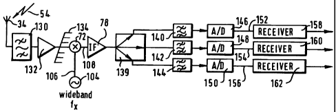
With regard to FIG. 4, an improved receiver path arrangement constructed
in accordance with a preferred embodiment of the present invention is
shown. For the purposes of explanation only, the preferred embodiment of
the present invention is described in relation to a receive module for a
CDMA communication network having three contiguous frequency carriers
spread across a five MHz bandwidth. In practice, this means that each
communication carrier nominally has a 1.25 MHz useable bandwidth
bounded by 0.675 MHz guard bands.
The preferred embodiment of the present invention utilises a single local
oscillator operable to convert received frequencies to intermediate
frequencies, whereby cross-talk between multiple synthesisers is
eliminated. In this respect, the present invention has a front end similar to
the wideband receiver chain of FIG. 3.
Nortel Confidential Proprietary
CA 02256287 1998-12-17
-14-
Looking in detail at the diagram of a preferred embodiment of the present
invention, incident RF signals 54 are received by antenna (such as main
antenna 34) and routed, via a radio frequency filter or diplexer 130 to an
amplifier 132. Received signals are amplified by amplifier 132 before being
fed to a six-way splitter 134.
As will be appreciated, use of diplexer (or circulator) enables the antenna to
be used for transmission as well as reception of suitably modulated RF
signals and accommodates the integration of a power amplifier into the
circuit, while the six-way splitter 134 provides representations of the
received signals to other reception paths within the base station. In this
latter respect, the six-way splitter 134 hence endows the base station with
an ability to provide a soft hand-over capability, whereby a mobile
communication device can be retained on an antenna of a particular sector
notwithstanding that the mobile communication device has, during an on-
going communication, moved from one sector to a different sector. In this
way, the communication system is seen to provide a seamless
transmission, during hand-over, while the communication system also
benefits from not having to implement excessive changeovers for mobiles
operating along sector boundaries.
Returning the FIG. 4, in a similar way to the prior art architecture of FIG.
3,
the preferred embodiment of the present invention utilises a single oscillator
104 that provides a mixing frequency 106 for application to a mixer 72.
The mixer 72 causes down-conversion of the incident RF signals 54 to an
acceptable band of intermediate frequency signals 108. Following down-
conversion, the band of intermediate frequency signals 108 can be
amplified in an intermediate frequency amplifier 78, with an output from the
intermediate frequency amplifier 78 being split (in a three-way splitter 139,
as appropriate) and individually applied to separate and distinct band-pass
filters 140-144. The individual band-pass filters each have a narrow
Nortel Confidential Proprietary
CA 02256287 1998-12-17
-15-
bandwidth that is centred about one of the assigned frequency carriers in
the assigned block of spectrum. The pass-band nature of each of the
individual filters 140-144 therefore isolates each frequency carrier prior to
an information bearing modulated signal of each carrier being digitised in
conventional (and relatively low cost) A/D converters 146-150, similar in
construction to the A/D converter of FIG. 1. Digitised representations 152-
156 of each of the information-bearing channel carriers are then applied to
individual and separate demodulators 158-162 for recovery of encoded
information.
The three-way splitter 139 will introduce a signal loss of 4.7dB, as will be
appreciated. Additionally, in relation to the architecture of FIG. 4, it will
be
appreciated that the three-way splitter coupled be substituted for a four
way-splitter in which one of its outputs is terminated to ground through a
suitable load, such as a resistor. Generally, the hybrid splitter arrangement
of FIG. 4 is realised by a succession of cascaded splitters that operate to
isolate the various frequency signals, with each successive cascade causing
additional signal loss proportional to the number of branches provided as
outputs from the splitter.
In relation to the construction of the in-line filters, a 1.25MHz bandwidth IF
filtering specification can be met by a low-loss, temperature-stable quartz
SPUDT-type SAW filter having an operating frequency of approximately
70MHz, while the downstream effects caused by intermodulation are
minimal. Additionally, the circuit can operate with a 30 decibel (dB) gain
between the antenna and each ADC (of which approximately half, i.e.
15dB, is required after the SAW device. Additionally, the filter should
preferably have performance rejection figures approximating to a -26dB
stopband beyond a t 1.25 MHz offset from mid-band (i.e. t 625 kHz from
the pass-band edges) and an attenuation of -80dB at the aliasing
frequencies. Generally, in-line ADCs, implemented as AD6600s, would be
Nortel Confidential Proprietary
CA 02256287 1998-12-17
-16-
clocked at 19.6608 MHz.
The architecture of FIG. 4 therefore provides a receiver module capable of
providing a receive radio frequency carrier selection for three contiguous
CDMA carriers covering, for example, a 3.75 MHz PCS allocation. Typically,
each relatively narrow bandwidth filters 110-114 is implemented as a SAW
device, while the A/D converters (or "ADCs") are implemented in
conventional ADC strip technology. Indeed, the circuit configuration of FIG.
4 is IS-97 compliant with a 10dB margin on single tone desens and spurious
intermodulation attenuation for up to three RF carriers, while the circuit
does not require that the entire 5MHz bandwidth (for a three carrier system)
be cleared prior to hardware deployment. Furthermore, the circuit maintains
effective operation (without impairment of reception capabilities) even in
the face of co-carrier interferers jamming any two of the available carriers
(in a three-carrier system).
The present invention therefore provides several advantages over a
wideband receiver in that multiple spectrum blocks can easily be provided
(subject to diplexer bandwidth limitations), while the arrangement is
inherently more compatible with initially uncleared spectrum. Specifically,
while the receiver module front end has a simplified single oscillator
arrangement, processing of the received signals and isolation of individual
frequency carriers, at an intermediate frequency, is achieved by discrete
chains comprising a narrowband filter, an A/D converter and a receiver
demodulator. These chains are easily manufactured on a modular basis, and
can be programmed (in accordance with known techniques) to address and
decode specific frequency carriers.
The packaging of the receiver modules further saves costs in that the co-
location of the filters and the ADCs is more easily fabricated, with the
filters
and the ADCs having a relatively low specification and hence a relatively
Nortel Confidential Proprietary
- --- ------------- - ---
CA 02256287 1998-12-17
-17-
low cost. Additionally, as a general consequence of the infrastructure being
relatively inexpensive, implementation of CDMA type technology is
encouraged. Moreover, the present invention provides several advantages
over single carrier receivers in that there is a lower cost and size for
carrier
counts of two or more (obtained through the elimination of duplicated
circuitry), with a close to cost parity with respect to single carrier usage.
A further enhancement to the basic principle of the present invention is
shown in FIG. 5. Rather than providing a common intermediate frequency
amplifier, intermediate frequency signals 108 are each feed through
separate paths (but at least two paths provided by a single, two-way
frequency splitter 169) to be amplified by parallel, wide bandwidth
intermediate frequency amplifiers 170-172 that feed separate receiver
branches 174-176, respectively. Again, it is only after intermediate
frequency amplification that the individual carriers are isolated by discrete
band-pass filters 178-188 which then feed dedicated A/D converters
assigned to each carrier (in an identical fashion to the arrangement of FIG.
4). Again, an auto-ranging IF-sampling ADC (such as the AD6600) would
be suitable fir use in the circuit of FIG. 5. The arrangement of the discrete
band-pass filters 178-188 in the separate receiver branches 174-176 is
structured such that the odd or even carriers are separated between each
of the receiver branches 174-176, i.e. each filter is separated from any
adjacent filter by a carrier spacing of one carrier. In other words, the
branches (and hence the receiver chains) are responsible for processing
non-sequential carriers. In this way, the enhanced structure afforded by
FIG. 5 ensures that the filters substantially do not interact by ensuring
that:
i) each filter characteristic has ostensibly tailed-off before cross-over of
adjacent filter characteristics; and ii) filter interactions caused by
reflections
from subsequent components in the receiver chain are minimised.
Since a frequency "gap" exists between adjacent channel filters, the
Nortel Confidential Proprietary
CA 02256287 1998-12-17
-18-
embodiment of FIG. 5 allows these filters to be driven, if desired, by a
single amplifier within each branch. Indeed, unlike the embodiment of FIG.
4 that typically realises the 3-way splitter 139 as a transformer-based
hybrid splitter, FIG. 5 has reduced signal loss as a consequence of merely
having to provide a conventional (non-hybrid) two-way split with 3dB signal
reflection.
The structure of FIG. 5 can therefore reduce manufacturing costs by
allowing the use of lower specification filters, while still providing a low
complexity solution. Particularly, the circuit arrangement of FIG. 5 is devoid
of a hybrid splitter, and so there is an associated cost saving and saving in
circuit board area. Additionally, the elimination of a hybrid splitter
prevents
a loss in signal power provided at an output stage of an amplifier associated
therewith.
Clearly, the concept behind FIG. 5 could be extended to provide three or
more separate receiver branches, with the isolation between each filter still
further improved by having a sequential assignment of carrier bands
between each set of filters fed from a common intermediate frequency
amplifier, i.e. a first common IF amplifier could serve carriers fi, f4 and
f7,
while a second common IF filter could serve carrier f2, f5 and f8, etc.
A further embodiment of the present invention is shown in FIG. 6 in which
intermediate frequency signals 108 are applied to different branches 174-
176 prior to being amplified in IF amplifiers 170-172. A first branch 174
includes a first band-pass filter 190 having a central operating frequency of
approximately 73.75 MHz and a bandwidth of approximately 1.25 MHz.
Following filtering, second carrier signals 192, centred about the operating
frequency of the first band-pass filter, are amplified in a first narrowband
amplifier 194 before being applied to a series combination of a filter 196, a
first ADC 198 and a second channel demodulator 200. In the second
Nortel Confidential Proprietary
CA 02256287 1998-12-17
-19-
branch 176, following IF amplification, amplified IF signals are applied to
parallel IF second 202 and third 204 band-pass filters. The second band-
pass filter 202 has a central operating frequency of approximately 72.50
MHz and a bandwidth of approximately 1.25 MHz, while the third band-
pass filter 204 has a central operating frequency of approximately 75.00
MHz and a bandwidth of approximately 1.25 MHz. Outputs from both the
second 202 and third band-pass filters are each applied to respective
variable attenuators 206-208. Following attenuation, the carrier signals are
combined at node 210 before being applied to a second narrowband
amplifier 212. First and third carrier signals 214 are then applied in series
to
a filter 216 and a second ADC 218. After conversion to digital
representations, first and third carrier signals are applied to discrete,
parallel
channel demodulators 220-222. In this way, the first and third carriers
share a common digitising circuit.
The first ADC 198 and the second ADC 218 are responsive to a clock 224
generating, for example, an operating frequency reference of 19.6608 MHz.
In the structure of FIG. 6, a central carrier (at 73.75 MHz) is digitised by
the first ADC 298, while carriers either side of this central carrier are
digitised in the second ADC 218. The filter characteristics for FIG. 6 are
similar to those described in relation to FIGs. 4 and 5. First and third
carrier
signals are summed together via the variable attenuators that function to
allow one of the filter outputs to be attenuated in the case of excessive
jamming.
Clearly, the variable attenuators of FIG. 6 could be substituted for switches
that function to terminate a signal path. Additionally, while separate ADCs
198 and 218 are shown, the skilled addressee will appreciate that, after
filtering and prior to digitisation, the carrier signals could be combined.
Consequently, one of the ADC could be eliminated provided that the
Nortel Confidential Proprietary
CA 02256287 1998-12-17
-20-
remaining ADC operated in a multiplexed fashion. Without using a faster
ADC, this configuration would however more an image closer to the pass-
band, and could therefore adversely affect attenuation.
Turning now to FIG. 7, a further embodiment of the present invention is
shown. FIG. 7 has a similar structure to that of FIG. 6, but all carriers
(from
both branches 174-176) are combined in a summing unit 240. Unlike the
configuration of FIG. 6, the second carrier signal applied to the first band-
pass filter 190 is also applied to a variable attenuator 242 in parallel with
the variable attenuators used for the first and third carriers. Following
summing of the signals in summing unit 240, a combined signal is applied
in series to an amplifier 246, a band-pass fiiter 248 that rejects image noise
(specifically by attenuating noise from amplifier 246 at image frequencies)
and an auto-ranging IF-sampling ADC 250. The ADC 250 then separates
individual carrier signals for application to respective channel demodulators
200, 220-222.
As will be appreciated, if the band-pass filters of FIG. 7 are realised by
SPUDT SAW filters (that do not have a linear phase), the circuit of FIG. 7
would require there to be an appropriate offset in the phases of the filters
to ensure that these phases aligned at the band edges of the filter
parameters. In this respect, for a two or three carrier design (having two or
three filters, respectively) this phase offset can be accomplished
independent of an absolute delay incurred through the band-pass filters.
Generally, the ADCs of the preferred embodiment of the present invention
all operate by over-sampling. As will be understood by the skilled
addressee, over-sampling is beneficial because it reduces filter cost by
reducing the effects of channel images from each of the individual band-
pass (carrier) filters. In the instances of a shared bank-end (occurring with
the recombination of the carrier signals, such as shown in FIG. 7), time
Nortel Confidential Proprietary
CA 02256287 1998-12-17
-21-
sharing of the receiver path is required
FIG. 8 is another variant based on FIG. 7. In the embodiment of FIG. 8
offers a programmable strip arrangement by providing programmable
switches for carrier isolation. Specifically, pairs of programmable switches
260-270 isolate the band-pass filters 280-284 from a receiver path, and
hence can eliminate the effects of a rogue mobile transmitting on one of the
carriers. The programmable switches 260-270 are typically operationally
responsive to a microprocessor 271 (with only one connection to switch
262 indicated for the sake of clarity). Furthermore, unlike the previous
embodiments, the band-pass filters 280-284 have differing bandwidths
ranging from approximately 1.25 MHz through 2.50 MHz to 3.75 MHz.
Consequently, the use of non-identical filters therefore requires accurate
matching of the phases of each filter.
FIG. 9 is a further enhancement of the basic structure of the embodiment of
FIG. 8, although in the case of FIG. 9 all band-pass filters revert to a
uniform bandwidth centred on each carrier frequency. Isolation of the
individual receive paths for each of the carriers is still achieved through
the
use of switches, although in this embodiment only a single switch is
provided after each band-pass filter 190, 202-204. To achieve a high
attenuation, the band-pass filters are arranged in branches that service non-
adjacent carrier signals, as in FIG. 5.
Briefly turning to FIG. 10, a flow diagram demonstrating a wideband signal
recovery mechanism for a preferred embodiment of the present invention is
shown. At step 280, incident carrier signals at relatively high frequencies
are received by the receiver (or transceiver) equipment. These incident
signals are down-converted 282 to respective (and relatively low-level)
frequency carriers by a common frequency down-converter. Following
generation of, typically, intermediate frequency signals (rather than
Nortel Confidential Proprietary
CA 02256287 1998-12-17
-22-
baseband signals), the low frequency carrier signals are preferably isolated
(in accordance with FIG. 5, for example) by applying non-sequential carriers
to different receiver branches (step 284). Individual (and frequency distinct)
low frequency carriers are then applied, at step 286, to dedicated receiver
chains having associated band-pass (or functionally equivalent) filters. Data
encoded within (i.e. modulated onto) the carrier can finally be recovered
(step 288) by associated channel demodulator/receiver back-end circuitry.
In summary, the present invention advantageously allows reception of a
block of radio frequency carriers in a single circuit module, while satisfying
the performance requirements of IS-97 on each individual radio frequency
carrier. Additionally, the preferred embodiment of the present invention
accomplishes isolation of multiple wideband carriers without requiring free-
configuration with respect to a number of carriers to be received, and
therefore addresses and resolves problems associated with uncleared
spectrum. Moreover, the present invention advantageously provides a
modular receiver that can be scaled for a frequency block allocation of 5
MHz or larger, e.g. 15 MHz. Furthermore, use of separate intermediate
frequency filters and separate A-D converters for each radio frequency
carrier eliminates the possibility of receive channel blocking problems when
operated in single or dual channel modes.
Clearly, the improved receiver path architecture of the preferred
embodiments of the present invention can be utilised within the generic
system configuration shown in FIG. 1.
It will, of course, be appreciated that the above description has been given
by way of example only and that modification in detail may be made within
the scope of the present invention. For example, while the preferred
embodiment of the present invention has been described in relation to a
CDMA system (and especially a PCS environment), the present invention is
Nortel Confidential Proprietary
CA 02256287 1998-12-17
-23-
clearly applicable to other communication systems, such as paging and
TDM systems and universal mobile telecommunication system (UMTS), that
have spectrum subsequently released or cleared for their use. Indeed, the
architecture of the present invention is particularly and equally suited to
other present or future protocols having 5 MHz-wide digitiser/carrier
modules and a universal frequency re-use pattern. Furthermore, while the
embodiments of the present invention have generally been in relation to a
three-carrier system, it will of course be appreciated that the concepts can
be extended to wideband and narrowband systems having two carriers or
more carriers that three.
The embodiments of the invention in which an exclusive property or
privilege is claimed are defined as follows:
Nortel Confidential Proprietary