Note: Descriptions are shown in the official language in which they were submitted.
CA 02256572 1998-11-30
WO 97/47481 PCT/US96/09888
DISPLAY UNIT AND METHODS OF DISPLAYING AN IMAGE
Field of the Invention
The present invention relates to a display unit, and in particular to a
display
unit for displaying images viewable from two sides, whereby the image as
perceived
from one side can be different from the image perceived from the other side
and the
display unit is transparent or translucent when viewed from one of the sides.
The invention also relates to a method of displaying such an image as well
as printers suitable for displaying a printed image and raster image
processing
(RIP) systems for preparing the data before display, particularly before
printing.
Background of the Invention
Display devices with differing images on each side and being transparent or
translucent from one of the sides are known from a variety of documents
including
EP-A-0170472 which describes a panel comprising a light permeable material and
a
silhouette pattern, comprising any arrangement of light restricting material
which
subdivides the panel into a plurality of discrete light restricting areas
and/or a
plurality of discrete transparent or translucent areas, characterized in that
a design is
superimposed on or forms part of said silhouette pattern so that said design
is
visible from one side of the panel only, and wherein said design is less
perceptible
from said one side of the panel as the level of illumination transmitted
through the
panel from said other side increases. A number of different vision effects are
obtainable from different panels failing within the above definition. Thus
clarity of
vision can be maintained from the one side to the other side with the
exception of
the area covered by the design with clarity of vision through the whole of the
panel
from the other side to the one side. Visibility from the one side to the other
side can
be totally or partially obstructed while there is clarity of vision through
the whole of
the panel from the other side to the one side, in other words a unidirectional
vision
effect is obtained. Clarity of vision is obtainable from the one side to the
other side
except in the area of the design while visibility from the other side to the
one side is
totally or partially obstructed. Vision from either side can be totally or
partially
-1-
CA 02256572 1998-11-30
WO 97/47481 PCT/US96/09888
obstructed. In all cases through vision can be obtained in either direction
through
the panel when the level of illumination perceived through the panel from the
far
side of the panel sufficiently exceeds the illumination reflected from the
near side of
the panel. The transparent areas typically have dimensions ranging from 0.5 to
3
mm.
EP-A-0170472 and EP-00l 18638 describe methods of producing both the
silhouette pattern and also the imposed design. The methods as described may
be
summarized as either sequential printing of the silhouette and/or the design
using
screen lithographic or similar ink printing processes with as exact a
registration as
can be obtained or a method in which a mask is applied and the printing
processes
are carried out through the mask onto the substrate. When the mask is removed,
the
silhouette pattern and image remain on the substrate only in the areas which
the
mask or stencil allow the ink to penetrate.
EP-A-0234121 describes further methods of printing such an image. The
printing methods are limited to those including inks. Again a mask is
described
which is subsequently removed taking with it unwanted portions of the
silhouette
pattern and image.
US-5396559 describes a security device for use on identification cards,
monetary documents, and the like using a reference pattern and a message
pattern
each having the appearance of a random pattern of dots. The reference pattern
is a
dense pattern of randomly positioned dots, and the message pattern is a
modulated
version of the reference pattern in which the dots of the reference pattern
are
slightly repositioned by an amount depending on the gray value or color value
of a
message image at each dot location. The message image is decrypted and becomes
visible with a range of gray values when it is viewed through a film
transparency of
the reference pattern. The dot pattern may be printed, embossed or recorded as
a
photograph or a hologram. Decryption of the message image may be accomplished
by viewing through a contact mask, superposition of images of the message
pattern
and reference pattern, by viewing the message pattern through a mask
positioned at
a real image of the reference pattern, or like means.
-2-
CA 02256572 1998-11-30
WO 97/47481 PCT/US96/09888
Japanese patent application Kokai 1 (1993) - 57863 describes a production
of an image including transparent sections for areas of the image. A method is
described in which a decorative sheet is prepared by registration printing in
the
order of a rear pattern layer, a covering ink layer and a front pattern layer
on a
transparent plastic sheet in such manner that a plurality of small transparent
portions
remain in the image. No description is made as to how the registration
printing
should be carried out.
Japanese patent application Kokai I(1989) - 69397 describes a method of
producing a transparent plastic or glass substrate with a printed layer
including a
plurality of holes. The method inciudes printing the image onto a second
substrate,
perforating the image and second substrate and then transferring the image
only
from the second substrate to the transparent plastic or glass substrate.
Summary of the invention
The present invention provides a method of displaying an image on a
display device having first and second sides, said image including a light
restricting
silhouette pattern having a plurality of first transparent or translucent
areas, and at
ieast one design layer having at least one colour, said at least one design
layer being
visible from one side of said display device and substantially less visible
from the
other side, said image being substantially transparent or translucent as
viewed from
the other side, comprising the steps:
1) providing at least a definition of said design layer to a computer;
2) generating a computerized version of said design layer with the computer;
3) outputting the computerized version of said design layer to said display
device, the computerized version of said design layer being modified to
subdivide
said design layer into a plurality of second discrete transparent or
translucent areas
and other areas, and
4) displaying said modified design layer and said silhouette pattern with said
first and second transparent areas being in registry.
-~-
CA 02256572 1998-11-30
WO 97/47481 PCT/US96/09888
The present invention also includes an article having a conformable
substrate, comprising: a coiorant receptor layer and a light restricting layer
on said
substrate, said light restricting layer having a plurality of first
transparent or
translucent areas.
The present invention also includes an article comprising: a polymeric
substrate having a composition comprising vinyl chloride resin, optional
acrylic
resin, optional plasticizer, and optional stabilizer, wherein the composition
is formed
on a polymeric release liner having smoothness of a Sheffield value of from
about I
to about 10, and a light restricting layer and a design layer on said
substrate, said
design layer including at least one color layer, said light restricting layer
being
subdivided into a plurality of first transparent or translucent areas, said
design layer
being subdivided into a plurality of second transparent or translucent areas,
and said
first and second transparent areas being in registry.
The present invention further includes a printer for receiving a print file
including color separated image data, light restricting layer data and
transparency
data, and for printing the color separated image and the light restricting
layer data
including transparent areas in both the color-separated layer and the light
restricting
layer in accordance with the transparency data.
The invention further includes a raster image processing method for raster
image processing of a print file including color separated image data, light
restricting layer data and transparency data, comprising: operating on said
print file
to generate raster image bitmaps for said color separated image data and said
light
restricting layer data, and introducing said transparency data into said
raster image
bitmaps for said color separated image data and said light restricting layer
data so
that the transparent areas in said color separated image raster bitmap and
said light
restricting layer bitmap are in registry.
The invention includes in addition a raster image processing system for
raster image processing of a print file including color separated image data,
light
restricting layer data and transparency data, comprising: means operating on
said
print file to generate raster image bitmaps for said color separated image
data and
said light restricting layer data, and means introducing said transparency
data into
-4-
CA 02256572 2006-03-07
60557-6011
said raster image bitmaps for said color separated image
data and said light restricting layer data so that the
transparent areas in said color separated image raster
bitmap and said light restricting layer bitmap are in
registry.
The invention also includes a graphics computer
based system for creating graphics images including color
separated layers and light restricting layers, comprising:
first input means for image data, means for generating color
separated image data from said image data, means for
generating light restricting layer data, second input means
for transparency data, and means for outputting a display
file including said color separated image data, said light
restricting layer data and said transparency data.
The present invention may provide conformable
articles including transparent areas in images, methods of
providing the same and printers, computer graphics systems
and raster image processing systems and methods for
producing images on the articles at low coast.
The present invention may provide conformable
articles including transparent areas in images, methods of
providing the same and printers, computer graphics systems
and raster image processing systems and methods for
producing images on the articles which allow variability in
image not previously achieved.
The present invention also provides a method of
preparing an image for display, said image comprising at
least two layers, including a light restricting silhouette
layer comprising an arrangement of light restricting areas
-5-
CA 02256572 2006-03-07
60557-6011
which subdivides the display into a plurality of discrete
light restricting areas and/or a plurality of discrete
transparent or translucent areas, and at least one design
layer having at least one colour which subdivides the
display into a plurality of discrete coloured areas and/or a
plurality of discrete transparent or translucent areas,
wherein the said coloured areas do not substantially
encroach onto the plurality of discrete transparent or
translucent areas of light restricting silhouette layer,
said at least one design layer being visible from one side
of said display and substantially less visible from the
other side, said display as a whole being substantially
transparent or translucent, the method comprising the steps
of: 1. using a computer for: providing at least a definition
of said design to a computer; and generating a computerised
version of said design with the computer; and further
comprising the step of: 2. computing data defining said
design layer from said computerised version of the design by
subdividing said computerised version of the design into
said plurality of discrete coloured areas and/or a plurality
of discrete transparent or translucent areas.
The present invention further provides a computer
based system for preparing and displaying an image for
display, said image comprising at least two layers,
including a light restricting silhouette layer comprising an
arrangement of light restricting areas which subdivides the
display into a plurality of discrete light restricting areas
and/or a plurality of discrete transparent or translucent
areas, and at least one design layer having at least one
colour which subdivides the display into a plurality of
discrete coloured areas and/or a plurality of discrete
-5a-
CA 02256572 2006-03-07
60557-6011
transparent or translucent areas, wherein the said coloured
areas do not substantially encroach onto the plurality of
discrete transparent or translucent areas of light
restricting silhouette layer, said at least one design layer
being visible from one side of said display and
substantially less visible from the other side, said display
as a whole being substantially transparent or translucent,
the system comprising: a computer having an input means for
inputting at least a definition of said design and a store
for storing a computerised version of said design; means for
computing data defining said design layer from said
computerised version of the design by subdividing said
computerised version of the design into said plurality of
discrete coloured areas and/or a plurality of discrete
transparent or translucent areas; means for computing data
defining said silhouette layer by subdividing a layer into
said plurality of light restricting areas and/or said
plurality of discrete transparent or translucent areas; and
means for generating a display file including the silhouette
layer data and the design layer data.
The invention with its embodiments and advantages
will be described with reference to the following drawings.
Brief description of the drawings
Figure 1 shows a schematic cross section of a
display unit in accordance with the present invention.
Figure 2 shows a block diagram of a display system
in accordance with the present invention.
Figure 3 is a complex image including transparent
areas in accordance with the present invention.
-5b-
CA 02256572 1998-11-30
WO 97/47481 PCT/US96/09888
Figures 4A and B show characters and shapes defined by transparent areas
in accordance with the present invention.
Figure 5 the graying effect of conventional light colored window graphics
as seen in the prior art.
Figure 6 shows a schematic cross-section view of a second embodiment of
a display unit in accordance with the present invention.
Figure 7 shows a cross-section view backlight for use with the second
embodiment of the present invention.
Figure 8 shows a schematic cross-section view of a third embodiment of a
display unit in accordance with the present invention.
Figure 9 is a cross-section through a printed substrate in accordance with
the present invention.
Figure 10 is a cross-section through another printed substrate in
accordance with the present invention.
Figure ] l is a cross-section view of a printing substrate in accordance with
a seventh embodiment of the present invention.
Figure 12 is a cross-sectional view of a of a printing substrate in
accordance with an eighth embodiment of present invention.
Figure 13 is a cross-sectional view of a printing substrate of a tenth
embodiment of the present invention.
Figure 14 illustrates a cross-sectional view of a durable, optically clear,
transparent layer of the eleventh embodiment of the present invention prepared
on a
polymeric release layer.
Figure 15 illustrates a cross-sectional view of the durable, optically clear,
transparent layer of the eleventh embodiment during a lamination step.
Figure 16 illustrates a cross-sectional view of the durable, optically clear,
transparent layer of the eleventh embodiment in combination with an imaged
substrate.
Figure 17 illustrates a cross-sectional view of the durable, optically clear,
transparent layer of the present invention in combination with an imaged
substrate
as a modification as a twelfth embodiment of the invention.
-6-
CA 02256572 1998-11-30
WO 97/47481 PCT/US96/09888
Figure 18 is a block diagram of the components of a printing system in
accordance with embodiments fourteen to sixteen of the present invention.
Figure 19A is a cross-section and 19B is a top view of a printed substrate
for use with embodiments fourteen to sixteen of the present invention.
Figure 20 is a schematic drawing of a printing head in accordance with the
fifteenth embodiment of the present invention.
Figure 21 is a schmatic drawing of a printer in accordance with another
embodiment of the present invention.
Definitions
As used in this application:
"colorant" means any material that imparts color to another niaterial or
mixture and maybe either, dyes or pigments,
"colorant receptor layer" means any layer on a printing substrate which is
provided for the purpose of transferring colorants to the substrate.
"durable" means the substrates used in the present invention are capable of
withstanding the wear and tear associated with signage and may be 2 to 5 years
in
exterior environments;
"plastic" means a material that is capabie of being shaped or molded with
or without application of heat and include thermoplastics types, thermosets
types,
both of which may be flexible, semi-rigid or rigid, brittle or ductile;
"smear-resistant" as used in this application means resistant of the ink jet
ink to smear as described in the following test, printing an image with black
lines,
allowing a minimum of five minutes time to dry, rubbing the line with the pad
of the
finger with a light to moderate pressure, such as might be used during normal
handling of images, and observing whether spread of the line occurs;
-7-
CA 02256572 1998-11-30
WO 97/47481 PCT/US96/09888
"durable" means the substrates useful in the present invention are capable
of withstanding the wear and tear associated with signage and may be used 2 to
5
years in exterior environments;
"conformable" means the substrates in a direct print film are capable of
conforming to uneven surfaces and retaining such conformation during use
without
significant force applied per unit area of the film. Typically the conformable
substrate can be adhered with hand pressure and conform to a surface having
periodic or compound irregularities, such as a rivet or welded ridge on the
exterior
metallic surface of a tractor trailer, without the substrate lifting from the
surface.
Preferably, a conformable substrate in a direct print film exhibits a yield
point and/or
permanent strain when subjected to a maximum tensile stress of about 3.5 X 10'
N/mz (5000 lb./square inch) at room temperature according to ASTM D638-94b
(1994), when the caliper used for the test includes the total cross-sectional
thickness
of the substrate, the thickness of the adhesive, and the thicknesses of any
further
layers such as ink receptor, conductive or dielectric layers. More preferably,
the
maximum tensile stress limit is about 1.4 X 10' N/M2 to provide more
conformable
films. Most preferably, the maximum tensile stress limit is about 7 X 10G N/M2
to
provide even more conformable films. Conformability of the films still require
internal integrity. Desirably, the minimum tensile stress limit is about 6.9 X
104
N/M2 (10 lb./scluare inch) and preferably the minimum tensile stress limit is
about
1.7 X 10⁵ N/M2 (25 lb./square inch) .
Testina Methods
Bulk Powder Resistivity: "The Application of ZELEC ECP in Static
Dissipative Systems" (Du Pont Chemicals, Deepwater, New Jersey September
1992)
Specific Resistance: "Tego Conduct S Resistivity Measurement and
Apparatus" (available from Esprit Chemical Company, Rockland, Maryland)
Surface Resistance: ASTM D 4496- 87 and ASTM D 257- 93 published
by American Society for Testing and Materials.
-8-
_ __...~
___.___
CA 02256572 2006-03-07
60557-6011
Color Shift; ASTM D 2244 - 93 published by American Society for
Testing and Materials.
Color Density: "Reflective Optical Density on a Status T Method" " under
the requirements of ANSI/ISO 5/3-1984, ANSI PH2. 18-1985 published by the
Graphic Communications Association of Arlington, Virginia. Reflected optical
density is measured using techniques well known to those in the printing
industry.
Examples herein were evaluated with a Gretag SPM50 densitometer from Gretag
Limited, CH-8105 Regensdorf, Switzerland. Other instruments will give similar
comparisons, but not necessarily the same values. "Color Density" is the
measure of
the intensity of the individual primary colors on a recording medium to form
the
latent image and is important to films of the present invention because color
density
has a major impact upon the perceived aesthetics of the image on the recording
medium. By comparison, transmission optical density may be measured using an
optical densitometer such as a Macbeth TD 904.
Sheffield: Sheffield method measurement described in TAPPI Test T 538
om-88 published by the Technical Association of the Pulp and Paper Industry of
Atlanta, Georgia.
Embodiments of the invention
The figures are intended for illustrative purposes only. Certain dimensions
may have been exaggerated to improve clarity.
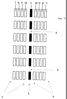
Figure 1 shows a schematic cross section through a display unit of the kind
used with the present invention. A display includes a first silhouette pattern
2,
comprising an arrangement of light restricting material which subdivides the
panel
into a plurality of discrete light restricting areas 5 and/or a plurality of
discrete
transparent or translucent areas 6. The light restricting areas 5 have light
transmission reducint', properties. These may be, in one extreme, completely
-9-
CA 02256572 1998-11-30
WO 97/47481 PCT/US96/09888
opaque, i.e. the optical density in transmission is infinite. Transmission
optical
density TOD (which is to be distinguished from reflection optical density,
ROD) is
defined by the formula:
TOD = logio C I~) ,
h
where I; is the intensity of the incident light on the sample material and I,
is the
intensity of the transmitted light passing through the material. The present
invention
accepts that the light restricting layer 5 may not be perfectly opaque but may
allow
some light to transmit. It is preferred if the TOD of the light restricting
layer is
greater than 1, preferably greater than 2, more preferably greater than 2.5
and most
preferably 3 or greater.
The translucent or transparent areas 6 allow light to pass through. In one
extreme the transparent areas 6 transmit all light and reflect or scatter no
light, i.e. a
TOD of infinity and a ROD of infinity, where the optical density in reflection
is
given by:
ROD = logiolh,
\IxJ
IR being the reflected light intensity.
The present invention accepts that the translucent/transparent areas 6 may
not be perfect light transmitters, i.e. they may absorb and/or reflect and/or
scatter
some light. It is preferred if the TOD of the transparent or translucent areas
have an
ROD of less than 1, preferably less than 0.5. The translucent areas 6 should
differ in
optical density from the light restricting areas 5 by a sufficient amount to
make a
clear visual difference. The TOD difference between areas 5 and 6 should
preferably
be greater than 0.3. According to the present invention the areas 6 are
preferably
transparent, more preferably optically clear.
The pattern of light restricting 5 and/or transparent/translucent areas 6 may
be any array of pixels, for example, a pattern of parallel lines, dots,
circles, squares,
etc. which niay be arranged in a regular array, in the form of a design , in
an
irregular array or in a random way. The transparent areas 6 may have any
-10-
CA 02256572 1998-11-30
WO 97/47481 PCTIUS96/09888
dimension depending upon the display device used, and may be diameters
typically
in the range of 0.1 mm to 8 mm, preferably 0.2 mm to 3 mm. The ratio of the
transparent areas 6 to light restricting areas 5 may be chosen as desired but
is
typically 0.3 to 3, usually about 1, i.e. 50% Of the surface area is covered
by
transparent areas 6. In accordance with the present invention the silhouette
pattern
2 may be provided by any spatial light modulator or filterwhich comprises a
plurality of discrete light restricting areas 5 and/or a plurality of discrete
transparent
or translucent areas 6. The spatial light modulator or filter 2 may be a
silhouette
pattern similar to that described in EP-A-0170472 or a pattern created by the
back-
light of a liquid crystal (LCD) display device or any other appropriate
display
device.
Substantially coextensive with the spatial light modulator or filter 2 is
placed a display device 3 and/or a display device 4. Display device 3 or 4 can
display an image which may be a full color image represented schematically by
the
four layers 7-10, 7'- 10' and the image is divided into transparent or
translucent
areas 6 and colored design areas 7-10,7'-10' so that the transparent or
translucent
areas 6 of the spatial light modulator or filter 2 are aligned (in registry)
with the
translucent or transparent areas 6 of display device 3, 4. The display device
3 or 4
may be a printed image, for instance, in accordance with EP-A-01 70472 or
similar,
or may be a LCD or LED display device which is capable of displaying a
monochrome or full color image. At least one of display device 3 or 4 may be a
black or dark colored pattern.
The display unit I may be self-standing or may be laminated to a substrate
such as a transparent sheet of glass-like or polymeric material. The glass or
polymeric sheet may be laminated to the display device 3, the display device 4
or
may be interposed between any of the layers 7-10,7'-10' or between display
device
3 and silhouette pattern 2 or between silhouette pattern 2 and display device
4. The
substrate may be the window of a car, bus or building or may be a flexible
polymeric sheet. When the display device 3 or 4 is black or a dark color and
is
located next to the transparent sheet 1, the dark display device 3, 4 may be
partly or
-11-
CA 02256572 1998-11-30
WO 97/47481 PCT/US96/09888
completely provided by tinting the transparent sheet as taught in EP Patent
No. 0
133 761.
Fig. 2 shows a schematic block diagram of the first embodiment of the
present invention. A suitable graphics image for display purposes is generated
in
image generation means 12. The image may be generated using computer 13 and
special software deveioped for production of graphic images such as Adobe
Photoshopl~" , Adobe IllustratorTM, Corel-DrawTM , Alduso PagemakerTM, Quark
XpressTM or similar. The image generation means 12 may be a scanner with which
all or part of picture information from an image, a picture or photograph is
converted point by point into electrical signals to be stored in computer 13
as digital
data.
Once the graphics image has been stored in computer 13 as a matrix of
digital data which include sufficient data to determine the luminosity and
color of
each pixel of information, the data may be prepared such that it may be
displayed
with a plurality of transparent areas 6 within the graphics image.
In accordance with the present invention this may be done in several
different ways:
Method 1. The color-separated layers of data (conventionally CMYK,
cyan, magenta, yellow and black or if the black layer is not used: CMY) may be
modified to include no color data representing the transparent areas 6 in each
of the
layers . This modification to the data may be done in computer 13 but the
invention
is not limited thereto. The pattern of transparent areas 6 may be provided by
overlaying the transparent areas 6 as areas of "no-color" onto the graphics
image
within computer 13. The no-color data may be stored as raster or pixel data.
In
general there is no need to modify the half-tone algorithms as disclosed for
instance
in US Patent Nos. 5,253,084; 5,258,832; 5,264,926; or 4,758,886 used to create
the full color image. However, if small diameters of the transparent areas are
used
(< 0.5 mm) it may be advisable to select the size of the transparent areas 6
and their
spacing so that they are not a multiple of the size of halftone cells in order
to avoid
rhythmic color shifts. With small size transparent areas 6, method 2 is
preferred.
The translucent/transparent areas 6 may be a regular, irregular, or random
array of
-12-
CA 02256572 1998-11-30
WO 97/47481 PCT/US96/09888
dots, lines, squares, circles, polygons, or similar, or a separate array of
these
representing a design or image. Both the size and the distribution of the
transparent
areas 6 may be varied through the image.
As shown in Fig. 3 the transparent areas 6 may be a complex and attractive
design 5, 6, 11 which has image portions 22 which may be light restricting and
a
transparent design portion 23 made up of transparent/translucent areas 6
surrounded by image areas which may be light restricting areas 5. The
transparent
areas 6 may have differing diameters and shapes in order to represent the
detail of
the design correctly. It is understood that on the reverse face of the design
22, 23, a
full color image 3 or 4 may be displayed. The representation of the filigree
patterns
of the fern leaves in a plurality of transparent areas 6 which are in registry
through
multiple layers of printing requires exact printing of small size repetitive
transparent
areas 6 separated by substantially opaque regions 5 in order to create a vivid
and
clear design.
] 5 Method 2. The data representing the transparent areas is stored in a
separate layer - a "T" layer - in computer 13. A display output file from
computer
13 includes the color separated primary printing color layers, CMYK or CMY
layers, plus the T layer. As will be described later, the information in the T
layer
may be used in different ways. For instance, where Raster Image Processing
(RIP)
is carried out, the data of the T layer may be introduced into each of the
CMYK
layers in the final raster bitmap during or immediately after the RIP.
Introducing this
data into the raster bitmap has the advantages that small repetitive structure
distortion may be reduced and the registration of the final image may be
improved,
as each color separated bitmap has the identical positions of the transparent
areas.
Alternatively, the T layer may bypass the RIP and be used by a display control
circuit to control the display 3,4 in such a way that the transparent areas 6
are
generated. For instance, where the display device 3,4 is a printer, the
transparent
areas 6 may be generated by activating or de-activating the printer head
during
printing in accordance with the T layer data.
Method 3. Method 3 is a modification of method 2 and uses a separate
transparent data layer T. The difference lies in the form of the data. In
accordance
-13-
CA 02256572 1998-11-30
WO 97/47481 PCT/US96/09888
with method 3, transparency data is stored in the same way as dot matrices are
stored, except instead of a dot representing a colored dot in the final
display the dot
represents a transparent area 6. All the techniques of word processing and
graphics
software can be duplicated in the inverse: instead of colored dots on a white
background, the data represents a transparent areas in a light restricting
background. For instance, the data may be stored as transparent fonts. Thus a
letter
such as "I" is stored in the computer as a character which includes a
predetermined
array of transparent areas 6 as shown schematically in Fig. 4A. When in the
"T"
mode, i.e. when generating the data for the transparency layer T, the key
stroke "I"
stores the array of transparent areas 6 shown in Fig. 4A. Similarly
transparency
graphic programs can be used to create designs in transparent areas. Thus
straight
lines or shapes may be generated. Graphic elements: a rectangle and a line of
transparent dots, are shown schematically in Fig 4B.
Method 4 is a modification to method I in which the silhouette layer 2 is
included in addition to the CMYK or CMY layers. The silhouette layer 2 may
generally be included as a light colored spot color, in particular, white. It
contains
the transparency data in registry with the transparency data in each of the
CMY or
K layers.
Method 5 is a modification of method 2 in which the silhouette layer 2 is
included in addition to the CMYK or CMY layers. The silhouette layer 2 may
generally be included as a light colored spot color. In preparing the
silhouette layer
2 for display, the same methods (e.g. RIP) may be used as described for the
CMYK
or CMY layers.
Method 6 is a modification of method 3 in which the silhouette layer 2 is
included in addition to the CMYK or CMY layers. The silhouette layer 2 may
generally be included as a light colored spot color. In preparing the
silliouette layer
2 for display, the same methods (e.g. RIP) may be used as described for the
CMYK
or CMY layers.
Method 7 is a modification to method 4 in which the image of display
device 4 is included in addition to the first image of display device 3 and
the
silhouette layei- 2. The second image may generally be included as further
CMYK or
-14-
CA 02256572 1998-11-30
WO 97/47481 PCT/US96/09888
CMY layers. These contain the transparency data in registry with the
transparency
data in all of the other layers.
Method 8 is a modification of method 4 in which the image of display
device 4 is included in addition to the first image of display device 3 and
the
silhouette layer 2. In preparing the second image 4 for display, the same
methods
(e.g. RIP) may be used as described for the CMYK or CMY layers of the first
image 3.
Method 9 is a modification of method 6 in which the image of display
device 4 is included in addition to the first image of display device 3 and
the
silhouette layer 2. In preparing the second image 4 for display, the same
methods
(e.g. RIP) may be used as described for the CMYK or CMY layers of the first
image 3.
For Methods 1-9, the image is output to a display device 14 which, in
accordance with the present invention, may be a direct display device similar
to an
LCD or LED display, an indirect printing device 16-19, or a direct printing
device
20, 21.
The method of displaying the data depends upon the method of storing the
data.
Methods 1, 2 and 7. As these methods have the transparency data stored in
each of the layers of the CMY1C or CMY data, the CMYK or CMY data can be
handled as in conventional display devices provided these can display the
number of
layers for the particular method.
Methods 2, 3 5, 8 and 9 include a separate "T" layer, which may be
processed by display devices according to the present invention. On some
existing
graphics software it may be possible to specify a transparent spot color or to
specify
a spot color of any desired color but modify the display device so that it
displays
this spot color as transparent. In accordance with this application, devices
capable
of processing data according to methods 2,3,5,6,7,9 are called transparency
layer
display devices or TLD devices.
When the display device 3 or 4 of Fig. 1 is viewed from the front and the
level of illumination on that side is high, the transparent areas 6 appear
dark,
-15-
CA 02256572 1998-11-30
WO 97/47481 PCT/US96/09888
normally black. If the image to be displayed is simply provided with
transparent
areas 6 without modification to the colors of the image, this image appears
uniformly darker than the original. This is particularly noticeable when the
display
device 3,4 is placed adjacent to the same image in which there are no
transparent
areas 6. This can occur when the display device 3,4 covers the window of a
vehicle
and the graphics continue onto the body of the vehicle. This is shown in Fig.
5
(Prior Art) which a photocopy of a photograph of a train in which large white
lettering has been applied over the side of the train. The white lettering
passes over
windows which have been covered with conventional punched film window
graphics. The gray appearance of the window areas 54 in comparison to the
adjacent areas 52 on the body of the train can be clearly seen. Hue changes
can also
occur in the arrangement such described with respect to Fig. 3 in which full
color
portions 22 of the image may be adjacent to portions 23 with transparent areas
6.
The following embodiment of the present invention provides a solution to this
problem.
The technique of undercolor removal is known in printing and
photography (see for example "The Reproduction of Color in Photography,
Printing & Television", Fountain Press, UK, Second Impression 1988). Instead
of
printing or displaying dark areas of the image with a combination of the three
traditional colors Cyan, Magenta and Yellow, using undercolor removal the
black
component of the color is provided separately, e.g. by using separate black
toners
or inks. In accordance with the present embodiment of the invention this
technique
is used in a novel way. When preparing the data for display, the computer
graphics
program of computer 13 of Fig. 2 carries out undercolor removal in the normal
way, however, the apparent dark color of the transparent areas 6 is taken into
account in the undercolor removal. For example, if 50% of the image area is
provided by transparent areas 6, a color with a black component of 50 + X %
will
be displayed with only a black component of X%. The color displayed is the
true
color as the remaining 50% black is provided by the transparent areas 6 which
appear black. For a color with less than 50% black, no black is displayed.
This
results in sonie darkening of the color with respect to the original but the
total
-16-
CA 02256572 1998-11-30
WO 97/47481 PCTIUS96/09888
effect is still improved. To prevent differences in hue between light colored
areas of
the image with and without transparent areas 6, the light colored areas of the
image
which do not have the transparent areas 6 (e.g. outside window areas or area
22 of
Fig. 3) are provided with additional black - in effect undercolor addition.
With the
example given above, if a color only has a 10% black component, this component
is removed as completely as possible from this color in the areas of the
transparent
areas 6. In parts of the image without transparent areas 6, this same color
has 40%
black added so as to match the hues throughout the image.
It is accepted that with some of the embodiments of the present invention
the display device 4 may be partly visible from the other side of the
silhouette layer
2, i.e. viewed from the side of display device 3. This may be due to the fact
that the
silhouette layer 2 can not be produced (e.g. by some kinds of printing
methods)
with such opacity that the display device 4 is totally isolated optically.
When display
device 4 has a dark color, the result of a light restricting but not opaque
silhouette
layer 2 is that all the colors of display device 3 become darker. In
accordance with
the present invention, any darkening of the image displayed on display device
3 is
also compensated for by undercolor correction, or if this is not possible, by
increasing the black content of any part of the image 3 which lies outside the
area
where there are transparent areas 6.
A further method of compensating for the darkening effect of the
transparent areas 6, is to partly metallize these areas. This has the effect
of reducing
transmission but provides a gain in reflected white light from the image 3. To
achieve metallization, the whole area of the substrate may be partly
metallized using
techniques known for two way mirrors.
A direct or simultaneous display device 15 in accordance with the present
invention is a display device which displays at least the image directly from
the
electrical output of the computer 13 and combines this with the silhouette
pattern 2
so that the transparent areas 6 of the silhouette layer 2 are in registry with
the
transparent areas of the image. Such a direct display device 15 in accordance
with a
second embodiment of the present invention is shown schematically in Fig. 6. A
conventional LCD display 24 is addressed by an addressing unit 28 which is
-17-
CA 02256572 1998-11-30
WO 97/47481 PCT/US96/09888
connected to the computer 13 in the conventional way e.g. by means of cable
and
connector 29. The LCD array 24 may form part of a window. Behind the LCD
array 24 is placed a back-light or reflector 25 which has a light source 26
connected
to a suitable power supply (not shown) by cable and connector 27.
The back-light 25 produces illumination in the form of strips, squares,
circles or similar shapes separated by areas of transparent material such as
to
produce the silhouette pattern 2 as shown in Fig. 1. An example of such a back-
light 25 is shown schematically in Fig. 7. The back-light 25 consists of a
series of
optical fibers 30 producing distributed light separated by transparent areas
31 which
may be a transparent material such as optically clear acrylic resin. The
optical fibers
30 are modified so that they distribute the light from the light source 26 and
emit
the light in a distributed way along their length in a direction perpendicular
to the
plane of the back-light 25 towards the LCD display 24. This may be done by
introducing an irregularity 32 called an optical element such as a slit, on
the surface
of each fiber 30 away remote from the LCD display 24. Such optical fibers 30
including optical elements 32 for producing a distributed series of cones of
light are
described in the article entitled "Control of light output from plastic
optical fiber
with optical elements" by Mary Poppendieck and David Brown, published at the
International Congress and Exposition of the Engineering Society for Advancing
Mobility Land Sea Air and Space, February 26-29 1996.
When the optical elements 32 are arranged on the side of each optical fiber
which is remote from the LCD display 24 then the individual cones of light are
reflected towards the LCD display 24 such as to illuminate parts, e.g. strips
or
rectangles of the LCD display 24. As explained in the above mentioned article,
the
25 spacing of optical elements 32 along the fiber 30 may be arranged so that
the
spacing of the elements 32 is closer together or intrude deeper into the fiber
dependent upon the distance from the light source 26. In this way, a uniform
extraction of light along the length of the fiber 30 may be achieved.
Further descriptions of how to produce a back light from optical fibers are
30 given in U.S. Pat. Nos. 5,226,105, 4,907,132; 4,885,663; 4,845,596;
4,519,017;
-18-
CA 02256572 2006-03-07
60557-6011
4,234,907, 5,432,876; 5,187,765; and 5,005,93 1.
The LCD display 24 is driven by the computer 13 via cable and connector
29 and addressing unit 28 so that only those iicluid crystal cells of LCD
display 24
which are illuminated by the optical fibers 30 are addressed with data of the
image 3
or 4 of Fig. I of the present application prepared in accordance with method 2
or 3
above. When the transparent areas are small, it is preferred if the
introduction of the
transparent areas in the data is delayed until immediately before display. For
instance, the output data file for the image on the display device is first
prepared in
the computer 13. Then the transparent areas 6 are introduced. It has been
found
that, particularly when the transparent areas 6 are small and are in a regular
array,
introducing the transparent areas at an earlier stage may result in distortion
of these
areas, when the image is manipulated by other algorithms, e.g. filters.
The under color removal mentioned above is carried out allowing for the
percentage of transparent areas 6 in the image 3,4 to be displayed. In the
areas of
the LCD display 24 which are opposite the transparent areas 31 of back-light
25,
the computer 13 outputs the relevant data so that the LCD display 24 is
transparent
in these areas. Thus the image 3,4 displayed on LCD display 24 consists of
areas of
the image 3 or 4 illuminated by optical fibers 30 separated by transparent
areas 31.
When viewed from the front of the LCD display 24, a full image 3 or 4 may be
seen
separated by the transparent areas 6 which appear dark when the general
illumination on the back-side of the LCD display 24 is lower than the general
illumination on the front side of the LCD display 24. On the other hand, when
viewed from the back of the LCD display 24, the display device 25 has
transparent
areas 31 separated by opaque areas provided by the back of the optical fibers
30.
In accordance with a modification of the second embodiment the back-
light 25 may be provided by a series of LED units 33 separated by transparent
areas
34 as shown in Fig. 8 schematically. The LED elements 33 may be formed in
lines
or squares or circles or in similar shapes and are arranged so that the light
emitted
from the LED elements 33 is projected towards the LCD display 24. Thus the LED
elements 33 illuminate those parts of LCD display 24 which contain image data
fed
-19-
CA 02256572 1998-11-30
WO 97/47481 PCTIUS96/09888
to the LCD display 24 via connector and cable 29 and addressing unit 28 from
the
computer 13. The data output from the computer 13 provides transparent areas
in
the LCD display 24 which are in registry with the transparent areas 34 of the
back-
light 25 shown in Fig. 8.
Alternatively, the display device 14 in accordance with a third embodiment
of the present invention may be an indirect printing device 16-19.
An indirect printing device in accordance with the present invention is a
printing method with which there is sequential colorant transfer of individual
color-
separated images from intermediate image carriers to the printing substrate.
Typically this requires a set of color-separated, i.e. single primary color,
intermediate image substrates 17 which are used in printing device 18 to
produce
the final printed iinage 19. The intermediate imaged substrates 17 are
produced
frorn the coniputer output data in the intermediate imaging device 16. Such an
indirect printing method may be for example lithographic or screen printing.
With reference to lithographic printing, the imaged substrates 17 may be a
series of imaged polyester lithographic plates, suitable for lithographic
printing on a
printing press 18. The lithographic substrates 17 may be generated directly
from the
information from the computer 13 in a suitable imaging device 16. The set of
lithographic substrates 17 may be used to print sequentially all or part of
the image
4, silhouette pattern 2 and image 3 of Fig. I in accordance with the present
invention. For instance, as shown schematically in Fig. 9, the image 4 may be
a
pattern of black 42 on a transparent sheet 41 in registry with an iight
restricting
white silhouette pattern 43 onto which is printed in registry a full 4-color
image 44-
47 leaving transparent areas 48. Data preparation may be performed by any of
the
methods 7 to 9 above. Thus, a total of 6 plates 17 may be necessary : black,
white,
cyan, magenta, yellow and black. An individual plate 17 may be used several
times
for each color in order to obtain sufficient depth of color or opacity of the
printed
layer 42-47 . Where a dark tinted transparent sheet 41 is used it may be
possible to
omit the first black layers and use only five coior layers: white, cyan,
niagenta,
yellow and optionally black. Data preparation may then be made in accordance
with any of the niethods 4 to 6 above. In order to obtain good registration
between
-20-
CA 02256572 2006-03-07
60557-6011
the various lithographic substrates 17, they may be produced by a method
described
in co-pending European patent publication no. EP 0741336 filed on May 4, 1995.
After preparation of the intermediate imaged substrates 17 from the image
data, the final prints 19 are produced in printers 18 in the conventional way
on clear
films. The printing films used for all the embodiments of the present
invention
involving printing are conformable due to the conformable nature of the
substrates
selected and tiie conformable adhesive layer contacting one major surface of
the
substrate.
An alternate sequence of color layers 42-47 may be printed as shown
schematically in Fig. 10. The order of the layers 42 to 47 is reversed and the
last
color printed is the black layer 42. As applied to a window substrate,
transparent
substrate 41 may now form the outer layer or overlaminate of the sheeting 40.
An
adhesive layer 50 may be applied optionally to the printed side of sheeting 40
in
order to secure the sheeting 40 to a window or similar. Adhesive layer 50 may
be
any of the adhesives mentioned below with reference to overlaminates. It is
preferred if the transparent substrate 41 of Figs 9 and 10 is the optically
clear vinyl
sheeting in accordance with the eleventh embodiment of the present invention.
It is
also preferred if the adhesive layer 50 is optically clear, preferably an
acrylic
pressure sensitive adhesive.
Although it is preferable to use a pressure-sensitive adhesive, any adhesive
that is particularly suited to the particular substrate selected and end-use
application
can be used on the sheeting 41. Such adhesives are those known in the art any
may
include adhesives that are aggressively tacky adhesives, pressure sensitive
adhesives, repositionable and/or positionable adhesives, hot melt adhesives
and the
like. Pressure sensitive adhesives are generally described in Satas, Ed.,
Handbook of
Pressure Sensitive Adhesives 2nd Ed. (Von Nostrand Reinhold 1989),
Also, as indicated in Fig. 10, any errors in registration between the printed
layers 42-47 may be compensated for by making the transparent areas 48 in the
silhouette pattern, i.e. the white layer 43, slightly smaller than in the
colored layers
-21-
CA 02256572 1998-11-30
WO 97/47481 PCT/US96/09888
44 to 47. Similarly, the transparent areas 48 in the black layer 42 may be
made
slightly smaller than the areas 48 in the white layer 43. By this means,
missregistration of the colored layers will not encroach into the transparent
area 48,
similarly missregistration of the white layer 43 will also not encroach into
the
transparent areas 48 of black layer 42.
The intermediate imaged substrates 17 may also be a set of screens for a
screen printing device 18. The output from computer 13 is then fed to an
automatic
screen producing device 16 as is known to a skilled person in screen printing
techniques. The final image 19 is produced by sequential printing of the
colors using
the screens 17 and conventional screen printing techniques.
A major disadvantage with indirect printing methods is that the
intermediate imaged substrates 17 are located in a printing device 18 in
sequence
and the maintenance of exact registration between the various layers of images
3
and 4 and silhouette pattern 2 of Fig. I is difficult or requires time
consuming
proofing and adjustment. Some improvement may be obtained by using a full
color
laser printer. In this case the intermediate imaged substrates 17 are provided
by the
imaged semi-conductive drums used to print substrates 19 by means of the
attraction of toner to the charged electrostatic areas of the drum. Providing
six or
more drums requires a special printer which is expensive, or in the
alternative, using
the same drum six times may make exact registration difficult. The AGFA
ChromapressTM electrostatic printing system supplied by AGFA-Gevaert NV,
Mortsel, Belgium, may be an indirect printer in accordance with the present
invention. The system includes 8 electrostatic printer drums arranged as a
series of
four drums on each side of the substrate to be printed. The printing drums are
controlled by a computer graphics system suitable for producing the modified
images in accordance with the present invention. This system is designed for
printing onto paper but could be modified to print onto clear films,
especially
optically clear polyester films of the type known for overhead transparencies.
It is preferred in accordance with fourth to sixteenth embodiments of the
method of the present invention if the display device 14 is a direct printing
device
20. In accordance with the present invention a direct printing device is
capable of
-22-
CA 02256572 1998-11-30
WO 97/47481 PCT/US96/09888
deposition of colorants of a full color image directly to a single printing
substrate.
The printing substrate may be the final printed article or an intermediate
substrate.
Hence a direct printing method is one which does not make use of a set of
intermediate imaged substrates 17 which must be used in sequence in order to
print
a substrate 19 in a printer 18. A direct printing device 20 in accordance with
the
present invention is able to convert the signals from the computer 13 into a
full
color image on a substrate 21 or a single intermediate substrate used for
transferring the image, e.g. a decal, in order to produce, for example, the
sheeting
40 shown schematically in Fig. 9 or 10.
Such direct printing methods may include but are not limited to, ink-jet
including bubble jet and spark jet, thermal and piezoelectric impulse jet,
thermal
transfer including sublimation or mass thermal transfer or electrostatic or
electrophotographic printing methods. In accordance with the present invention
a
direct printing method may also be the electrostatic transfer method known as
ScotchPrintT" Electronic Graphics System available from Minnesota Mining and
Manufacturing Company in which an electrostatic image is first created on
special
electrostatic paper and then is transferred in a single operation to a
transparent
substrate 21. The distinction between the ScotchPrintTM process described
above
and the indirect printing methods such as screen printing or lithographic
printing is
that the transfer of the image is carried out with a single substrate and is
in full color
whereas the indirect printing methods make use of a set of color separated
imaged
substrates 17 in order to generate a full color image. The registration of
electrostatic printing may be considerably better than that of an indirect
printer
method, independent of whether the transfer process is used.
An example of a printing process used in the present invention comprises
feeding the niaterial 41 in either sheet form or dispensed from a roll into a
printer,
printing a desired color image and silhouette pattern 42-47 in accordance with
the
present invention, retrieving the image from the printer and, optionally,
overlaminating the image with a film 50 to protect the receptor coatings and
image
from water, scratching and other potential sources of damage to the iniage,
and
-23-
CA 02256572 1998-11-30
WO 97/47481 PCT/US96/09888
then removing the release liner, and affixing the printed image to a
transparent
substrate for viewing.
It is preferred if the direct printing method has good local registration. An
example of good local registration printing is that produced by a conventional
high
quality ink-jet printer which prints relatively local areas of full color.
Thus, very
high quality registration can be obtained locally on the receptor niedium. As
very
high definition is required around each small transparent area in the image,
good
local registration may be advantageous and some distortion of the complete
image
over long distances may be toierated. On the other hand, electrostatic
printers have
distances of several centimeters between each color station so that full color
printing is not carried out as locally as ink jet printers, even with single
pass
machines.
Many factors may affect the iocal registration of printing. Ink jet printers
move the substrate a distance of 2- 3 mm between colors, whereas a single pass
electrostatic printer moves the substrate between 100 and 150 mm and a thermal
transfer printer such as the Summagraphics SummachromeTM Imaging system prints
the whole area before changing color. Tests have indicated that the amount of
movement between color changes is not a reliable guide to the degree of local
registration.
Printers are often characterized by "dots per inch" or DPI. Tests have
indicated that DPI is a better guide but not an infallible one for the choice
of printer
in accordance with the present invention as can be seen from Table I below.
Warp or distortion or thermal expansion/contraction of the substrate 21 or
of intermediate substrates 17 may also affect or reduce the theoretical level
of local
registration.
It has been determined that the degree of local registration can be
determined practically by printing a special test image which includes a
special full
color image with a regular array of transparent circles of different
dianleters in the
image. When the diameter of a transparent area drops below a certain value,
the
errors in printing registration are such that individual transparent areas are
reduced
significantly in diameter.
-24-
CA 02256572 1998-11-30
WO 97/47481 PCTIUS96/09888
The special test image is preferably constructed of all the layers to be
printed and each layer being printed at 100% color. Each layer includes the
pattern
of transparent circles with decreasing diameter in registration with every
other
layer. As an example, layers of the colors black, white, magenta, yellow, cyan
and
black are printed at 100% color intensity sequentially, each layer including
the array
of transparent circles. As the colors are at 100%, any missregistration will
be easily
visible as the respective color encroaching into the transparent areas and
reducing
their diameters.
In accordance with the present application, the "locai registration index"
(LRI) of the printing method/printer involved, is defined as the transparent
area
diameter in mm at which the diameter of a substantial number of the
transparent
areas in the printed image has reduced to 50% of its intended diameter in any
direction. Typical values are given in Table I for some commercial printers.
Actual
values of LRI depend on the accuracy of setting up the printer and of
calibration. It
is advantageous if the printer in accordance with the present invention has a
local
registration index (LRI) better than (i.e. less than) 1.0 mm and preferably
less than
0.6 mm and more preferably about 0.3 mm when printing 4 or more colors.
Table 1
Printer Type LRI print DPI
(mm) ualit
Encad Novajet Thermal Ink jet 0.6 excellent 360
SummaChromeTM, Thermal transfer -0.4* excellent 406
Summa ra hics Corp.
DesignJetTM HP750C Thermal Ink jet -0.4* excellent 360
Hewlet Packard Corp.
Xerox 8954 Electrostatic 0.7 good 200
multipass
3M ScotchPrintTM 9512 Electrostatic, one 0.6 good 400
pass
Raster Graphics Inc. Electrostatic, 1.0 good 200
DCS 5400 multi-pass
* The quality of printing was very good that it was difficult to determine the
limit
due to extraneous effects probabiy introduced by the graphics software.
-25-
CA 02256572 1998-11-30
WO 97/47481 PCT/US96/09888
Generally, the silhouette pattern 2 includes an light restricting light
colored
or white layer or metallic silvery or gold layer which faces the display
device 3
and/or the display device 4 of Fig. 1. In accordance with the present
invention, this
light restricting light colored layer 2 may be printed using light colored,
silver
metallic or white ink or toner depending on the printing method used. A white
spot
color is preferred. "Light restricting" means that the deposited layer has a
transmission optical density (TOD) of at least 1.0, preferably of at ieast
2.0, more
preferably of 2.5 and most preferably of 3.0 or greater. The software required
for
computer graphics using computer 13 in accordance with the present invention
is
modified so that areas of white are printed with the white toner or ink as a
spot
color, whereas the transparent areas are "printed" as "no ink" areas.
To prepare the data for the graphics design, the image 3,4 may be first
created and stored in computer 13 including data for a light restricting layer
43.
Under-color removal in accordance with the invention may be carried out on the
image data as described above. The image is normally stored as color separated
layers or planes of data for each primary printing color. Each of the planes
represents the data for one color, e.g. black, cyan, magenta or yellow or a
spot
color. With conventional equipment, data preparation method 7 is used and the
following is created: a 100% black or dark colored plane of data representing
layer
42 as the first image 4 within the graphics software. This may be created as a
spot
color layer. Next, a 100% white, silver or light colored plane of data
representing
light colored layer 43 as the light restricting layer 2 is produced. Finally,
the data for
layers 44-47 as the full color graphics image 3 is generated. The black and
white
layers 42, 43 are preferably specified as spot colors. This results typically
in
producing 6 sets or pianes of data: one for the black layer 42, one for the
white
layer 43 and four for layers 44-47 of magenta, yellow, cyan and black used for
a
full-color print. However, the invention is not limited thereto. Where a good
quality
process black may be produced, i.e. a black from a mixture of cyan, magenta
and
yellow, the final black layer 47 may be omitted. Where a tinted substrate is
used the
first black or dark layer 42 may be omitted. One or more of the layers 42-47
may be
-26-
CA 02256572 1998-11-30
WO 97/47481 PCT/US96/09888
applied as a plurality of layers. For instance, the white layer 43 may be
stored as a
series of planes of data representing white layer 43 in order to obtain
sufficient
opacity in the final print.
The array of transparent areas 48 may be generated within computer 13
and the image data modified by introducing the transparent areas 48 into each
of the
layers of data representing the printed layers 42-47 by overlaying or other
technique. Typically f o r printing devices 16 - 21, "EPS" Separation files
are
constructed from the modified image including the transparent areas 48 and
these
files are communicated to the relevant intermediate imaging device 16 or
printer 20.
Alternatively and preferably, the introduction of the transparent areas 48
into the
data to be printed is delayed to the last possible step before creation of the
intermediate imaging substrates 17 or printing to form printed images 21. This
is
best achieved using data preparation methods 5,6,8, or 9 in which a separate T
layer
is output from the computer 13. The T layer data is introduced into the CMYK
layer data and the silhouette layer data when the output data from the
computer 13
is raster image processed into raster bitmaps of the various print layers 42-
47. This
has the advantage that operating on the data with algorithms, e.g. to prepare
print
files, change scale, change from Macintosh format to DOS format, is carried
out
before small scale repetitive structures such as the transparent areas 48 are
introduced into the image data. Due to truncation errors, small scale
repetitive
structures in digital data may suffer distortions when operated on by
algorithms.
Such distortions may appear as rhythmic changes of size or shape or loss of
part of
the image.
To protect the printing, a transparent overlaminate 49 may be used which
is preferably optically clear. It is preferred if the overlaminate 49 is the
optically
clear sheeting in accordance with the eleventh embodiment of the present
invention.
In this application, overlaminate layer 49 refers to any clear material that
can be adhered to the surface of any existing coated or uncoated sheet
material.
"Overlamination" refers to any process of achieving this adherence,
particularly
without the entrapment of air bubbles, creases or other defects that might
spoil the
appearance of the finished article or image.
-27-
CA 02256572 1998-11-30
WO 97/47481 PCT/US96/09888
The deleterious effects of ambient humidity may be slowed by the
overiamination of a transparent protective coat or sheet herein referred to as
an
overlaminate. Overlamination has the further advantage that the images are
protected from scratching, splashes, and the overlaminate can supply a high
gloss
finish or other desired surface finish or design, and provide a degree of
desired
optical dot-gain. The overlaminate layer 49 may also absorb ultraviolet
radiation or
protect the underlayers and image from deleterious effects of direct sunlight
or
other sources of radiations. Overlamination is, for example, described in US
patent
4,966,804.
After printing an image or design of the present invention, the image is
preferably overlaminated with a transparent colorless or nearly colorless
material
49. Suitable overiaminate layers 49 include any suitable transparent plastic
material
bearing on one surface an adhesive. The adhesive of the overlaminate layer 49
could be a hot-melt or other thermal adhesive or a pressure-sensitive
adhesive. The
surface of the overlaminate layer 49 can provide high gloss or matte or other
surface texture. Preferred overlaminate layers 49 are designed for external
graphics
applications and include materials such as those commercially available from
3M
Company as ScotchprintTM 8910 Exterior Protective Film, 8911 Exterior
Protective Film, and 8912 Exterior Protective Film. However, other films are
available or could be fabricated and the invention is not limited to those
exemplified.
In the absence of the use of a clear, transparent overlaminate, a protective
clear coat of a vinyl/acrylic material may be applied, such as Product Nos.
3920,
8920, 9720, 66201, and 2120 protective coatings from the Commercial Graphics
Division of Minnesota Mining and Manufacturing Co. of St. Paul, USA to protect
the durable, imaged substrate. Such coating may be performed by some printers
at
the end of the image printing process.
Pressure sensitive adhesives useful for layer 41 can be any conventional
pressure sensitive adhesive that adheres to both layer 4 1 and to the surface
of the
item upon which the sheeting 40 having the permanent, accurate image is
destined
to be placed. Pressure sensitive adhesives are generally described in Satas,
Ed.,
-28-
CA 02256572 2006-03-07
60557-6011
Handbook of Pressure Sensitive Adhesives 2nd Ed. (Von Nostrand Reinhold
1989), Pressure sensitive
adhesives are commercially available from a number of sources. Particularly
preferred are acrylate pressure sensitive adhesives commercially available
from
Minnesota Mining and Manufacturing Company of St. Paul, Minnesota and
generally described in U.S. Pat. Nos. 5,141,790, 4,605,592, 5,045,386, and
5,229,207.
Non-limiting further examples of pressure sensitive adhesives useful with
the present invention include those adhesives described in U.S. Pat. Nos. Re.
24,906 (Ulrich), 2,973,826; Re. 33,353, 3,389,827;4,112,213; 4,310,509;
4,323,557; 4,732,808, 4,917,929; and 5,296,277 (Wilson et al.) and European
Publication 0 051 935.
A presently preferred adhesive is an acrylate copolymer pressure sensitive
adhesive formed from a 90/10 weight percent monomer ratio of 2-methylbutyl
acrylate/acrylic acid in a 65/35 heptane/acetone solvent system (39-41%
solids) and
having an inherent viscosity of about 0.7-0.85 dl/g.
Thickness of adhesive 318 can range from about 0.012 mm to about 1 mm
with a thickness of about 0.025 mm ( l mil) being preferred.
The adhesive may be protected with an optional liner (not shown) which
can be constructed from any conventional release liner known to those skilled
in the
art for image graphic media. Non-limiting examples include PolyslikT"" release
liners
commercially avaiiable from Rexam Release of Oak Brook, Illinois and polyester
liners such as a 0.096 mm polyethylene terephthalate film with a matte
backside
coating on one major surface and on the other major surface, a vanadium
oxide/surfactant/sulfopolyester antistatic primer coating and a condensation
cure
silicone exterior coating. These antistatic coatings are generally described
in U.S.
Pat. No. 5,427,835 (Morrison et al.).
Ideally the liner is optically flat. The liner preferably has a Sheffield
value between 1 and 10.
Non-limiting examples of further release liners include silicone coated
Kraft paper, silicone coated pofyethylene coated paper, silicone coated or non-
-29-
CA 02256572 2006-03-07
60557-6011
coated polymeric materials such as poiyethylene or polypropylene, as well as
the
polymeric materials coated with polymeric release agents such as silicone
urea,
urethanes, and long chain alkyl acrylates, such as defined in U.S. Pat. No.
3,957,724; 4,567,073; 4,313,988; 3,997,702; 4,614,667; 5,202,190; and
5,290,615,
In accordance with the present invention the transparent areas in the
printing may be introduced after the RIP. The printer 20 or the intermediate
imaging device 16 may be a "TLD" device configured to introduce the
transparent
areas of the image. For instance when printer 20 is an inkjet printer, the
printer may
be configured so that no printing is carried out for the whole width of a
printing
substrate at regular intervals. This produces a series of parallel transparent
areas.
Alternatively the printing head may be deactivated a repeated number of times
to
produce a distribution of square or rectangular transparent areas. If the
printer 20 is
an electrostatic printer, portions of each printing head may be missing or
deactivated, which produces a series of longitudinal transparent areas.
Portions of
the heads may be deactivated in sequence to introduce square or rectangular
transparent areas.
A TLD printer in accordance with the present invention may be created by
control of the printer 20 using the T layer data. After raster image
processing, the
raster bit maps may be operated on by a further algorithm using the T layer
data
which changes the raster bit map such that transparent areas are produced when
printed. Such a modification may be done by a hard-wired circuit in the
printer 20
or by software run on a local processor in printer 20. Alternatively, the T
layer data
may be used to control the printing head directly. For instance, for an ink
jet printer
the print signals going to the printing head may be suppressed in accordance
with
the T layer data to produce transparent areas at the required positions.
In accordance with the fourth embodiment of the present invention the
silhouette pattern 2 and images 3 or 4 are printed using ink-jet or bubble jet
printing methods. Ink-jet printing includes a variety of procedures including
thermal
ink-jet printing and piezo-electric ink-jet printing. All these methods have
in
common that discrete quantities of ink are sprayed from fine nozzles towards a
-30-
CA 02256572 1998-11-30
WO 97/47481 PCT/US96/09888
receptor sheet. Recently, wide format printers have become commercially
available,
and therefore the printing of larger articles such as large engineering
drawings,
blueprints and color posters and signs has become feasible. Suitable receptor
sheeting for non-durable use may be transparent polyester marking film
8501/8501H, supplied by Minnesota Mining and Manufacturing Company. The
optically clear, flexible vinyl substrate in accordance with the eleventh
embodiment
is particularly preferred. The formation of accurate inkjet images is provided
by a
variety of commercially available printing techniques. A suitable large format
printer, including warranted clear films and inks is the Hewlett Packard HP
Design
Jet 750C or 755CM printer, supplied by Hewlett Packard Corporation of Palo
Alto,
California, USA, however, may other brands are available. Non-limiting
examples
include thermal inkjet printers such as DeskJet brand, PaintJet brand,
Deskwriter
brand, DesignJet brand, and other printers commercially available froni
Hewlett
Packard Corporation as well as piezo type inkjet printers such as those from
Seiko-
Epson, spray jet printers and continuous inkjet printers. To perform the
invention,
additional cartridges should be added to the printing head in addition to the
usual
four colors, cyan, magenta, yellow and black. To print a black layer 42 and a
white
layer 43 of Figs. 9 or 10, at least an additional white station and black
station are
required. To obtain good opacity two or more white or black cartridges may be
added to the printing head.
From the test results shown in Table 1, it can be seen that ink jet printing
provides highly accurate local registration printing. Pigmented ink jet
printing inks
are available from the Commercial Graphics Division of Minnesota Mining and
Manufacturing Company (3M). Generally, pigmented ink jet inks from 3M a water-
based pigmented ink which comprises a suspension of commercially available
pigment particles and a dispersant of a formula of
-31-
CA 02256572 1998-11-30
WO 97/47481 PCT/US96/09888
3
H ~ C02R2a
R N C02R21
R5 4
m
wherein R is an alkyl, aryl, or aralkyl group obtained by the removal
of primary amino groups from alkyl, aryl, or aralkyl amines;
m =1 to6;
R'' and R'' are hydrogen or lower alkyl;
R' is the residue of the nitrogen reactive compound selected from
the group consisting of acylating reagents, carbamoyl halides, sulfamoyl
halides,
alkylating reagents, alkylating (epoxide) reagents, iso(thio)cyanates,
sulfonating
reagents, and aziactone reagents;
wherein R20 and R21 are independently, alkyl, aryl, or aralkyl groups,
or a cation selected from the group consisting of a proton, lithium, sodium,
potassium, ammonium, or tetraalkyl ammonium.
Pigments for ink jet inks use the standard colors of cyan, magenta,
yellow, and black.
For black inks, carbon black can be used as the black pigment. The
selection of carbon blacks suitable for use with the present invention is
based
primarily upon considerations of surface oxidation (high "volatiles"
preferred), and
the degree of blackness (also called jetness) of the pigment. Pigments that
are acidic
or surface-treated provide suitable interaction sites for strong dispersant
adsorption.
Pigments having a high surface oxide content are more hydrophilic, and thereby
much easier to disperse. Pigments with a high degree of blackness orjetness
provide a high quality printed image.
For yellow inks, the use of nickel azo yellow pigment offers several
advantages. First, such pigments provide inks which are highly durable in
outdoor
environments. Second, such pigments contain nickel ions which may be able to
form complex bonds with the novel dispersants. Lastly, such pigments are
believed
-32-
CA 02256572 1998-11-30
WO 97/47481 PCT/US96/09888
to offer a high degree of thermal conductivity. As a result, if particle
deposition
onto a heater element does occur during the jetting process, the deposited
film will
not significantly reduce the heating efficiency of the ink, thereby allowing
proper
bubble formation. For magenta inks, a primary consideration is lightfastness,
since it is very desirable to produce graphic images that are adapted to
outdoor
applications. Quinacridone magenta pigment is known to have excellent
lightfastness, and therefore, is one preferred magenta pigment.
For cyan inks, the considerations above, (i.e., lightfastness, durability,
etc.),
apply as well. As a variety of satisfactory properties may be found using
copper
phthalocyanine as a cyan pigment, inks comprising such pigments are one
preferred
embodiment.
Preferably, pigmented ink jet inks can be prepared with dispersants of the
following formula.
R3
H -C - CO 2R e
R N C CO yR 10
R4
H
N X (CH 26 *"'Y NR' IRB
---,.-fy R5
O Rs R O
m
Specific compositions of suitable dispersants are given in the Tabie below.
Ex R* R' R-' R R' R R" R9 R'" R1 n
i
a R H H H CH, CH3 C4H9 Na Na H 2 0
b R H H H CH3 CH3 CRH,, Na Na H 2 0
c R H H H CH3 CH, C, ,H,; Na Na H 2 0
d R H H H CH3 CH, C1KH3- Na Na H 2 0
c R H H H CH, CH3 CH,CH,Cr,H; Na Na H 2 0
f C,H,CH-CH- H H H CH, CH, C.,Hq Na Na H 1 0
g N(CH2CH_-); H H H CH3 CH3 C.,H9 Na Na H 3 0
h R H H H CH3 CH, R** C2HS CZH, H 2 0
R H H H CH, CH3 R*** C2HS C,Hs H 2 0
-33-
CA 02256572 1998-11-30
WO 97/47481 PCT/US96/09888
*The aspartic ester used in the preparation of the dispersant of examples a-e,
h and j
was DesmophenTM XP 7059E, available from the Bayer Corporation, Pittsburgh,
PA. DesmophenTM XP 7059E contains a short chain alkyl group.
**The amine used in the ring opening reaction to prepare dispersant of Example
h
was JeffamineTM M-600 [O-(2-aminopropyl)-O'-(methoxyethyl)polypropylene
glycol 500] (available from Fluka Chemical Corp. Ronkonkoma, NY).
***The amine used in the ring opening reaction to prepare dispersant of
Example j
was JeffamineTM M- 1000 [O-(2-aminopropyl)-O'-(2-methoxyethyl)copoly(ethylene,
propylene glycol 900] (available from Fluka Chemical Corp. Ronkonkoma, NY).
In the practice and the field of the fifth embodiment, the groups which are
not directly involved in the reaction steps forming the compounds of the
present
invention may be substituted to meet desired physical property requirements in
the
final dispersants. This is not only allowable, but may be highly desirable or
essential
in the formation of tailored dispersants. Where individual substituents may
tolerate
such broad substitution, they are referred to as groups. For example, the term
"alkyl group" may allow for ester linkages or ether linkages, unsubstituted
alkyls,
alkyls with such useful substitution as halogen, cyano, carboxylic ester,
sulfonate
esters or salts, and the like. Where the term "alkyl" or "alkyl moiety" is
used, that
term would include only unsubstituted alkyls such as methyl, ethyl, propyl,
butyl,
cyclohexyl, isooctyl, dodecyl, etc.
In addition to the pigments and dispersants described above, the inks will
comprise primarily water as a pigment suspension agent. Such inks will
typically
also include further additives to provide various properties. For example, an
alcoholic polyol, may be employed to control the drying rate of the ink.
Suitable
alcoholic polyols include, for example, polyalkylene glycois such as
polyethylene
glycol and polypropylene glycol; alkylene giycols whose alkylene group has 2-6
carbon atoms, such as ethylene glycol, propylene glycol, butylene glycol,
triethylene
glycol, 1,2,6-hexanetriol, thiodiglycol, hexylene glycol, and diethylene
glycol,
glycerol; and lower alkyl ethers of alcoholic polyols such as ethylene glycol
monomethyl or monoethyl ether, diethylene glycol methyl or ethyl ether, and
triethylene glycol monomethyl or monoethyl ether. A surfactant, useful for
wetting
and reducing the surface tension of the ink system, can be provided as well.
In
-34-
CA 02256572 1998-11-30
WO 97/47481 PCTIUS96/09888
addition to the above, other ink additives commonly known in the art may also
be
used. These include, water-soluble organic cosolvents, humectants, biocides,
fungicides, defoamers, corrosion inhibitors, viscosity modifiers, pH buffers,
penetrants, sequestering agents, and the like.
Current compounding technology for the processing of pigment
dispersions employs numerous processing technologies. One such technology
makes use of ultrasonic energy to achieve mixing and particle deflocculation.
Another technology makes use of media mills, such as ball mills, sand mills or
attritors. Media mills achieve acceptable pigment dispersions by subjecting
the
pigment mixture to high intensity microshearing and cascading which breaks
down
agglomerations of the pigment particles. However, media mill processing
systems
often suffer from disadvantages including media wear product contamination.
Additionally, if the flow rate in a media mill is raised beyond a certain
level, the
resulting grinding and dispersion becomes uneven, and much of the material
leaves
the system without being sufficiently processed.
Problems associated with media milling systems can be overcome, at least
in part, using homogenizers and emulsifiers. These systems generally function
by
forcing a premix of solids and liquids to collide against a surface, or to
collide
against itself. Unfortunately such high pressure devices are considered to be
unsuitable for processing pigment dispersions due to the abrasive nature of
the
pigment particles and the relatively large size of pigment agglomeration
structures
which can plug narrow gaps through which such systems force the mixture being
treated. Such clogging can be avoided, at least in part, by filtration or
preprocessing to reduce the size of pigment agglomerations and to ensure
sufficient
dispersion of the pigment prior to use of high pressure processing.
In still another processing method, the pigment dispersion can be forced
through a series of small nozzles having diameters on the order of about 150
micrometers to about 1000 micrometers. Such systems must be able to withstand
very high pressures at high fluid velocities. Three different configurations
for such
systems may be used: a) a "wedge" configuration with orifices of decreasing
diameter, b) a "wedge" configuration within which the orifices have cavitation
-35-
CA 02256572 2006-03-07
60557-6011
enhancement devices, and c) an "impinging jet" configuration in which the
dispersion stream is split into at feast two elements, each stream is passed
through
an orifice to create a jet, and the jet streams are recombined by impinging
them
against each other. Each of these systems has been found to yield satisfactory
results when processing water-based pigmented inks,
After the ink has been processed using either of the "wedge"
configurations or the "impinging jet" configuration at a concentration of
about 15
% by weight, it is diluted with an additional amount of deionized water and
diethyiene glycol to produce a final ink concentration of about 4 %
concentration
with a given diethylene glycol-to-water ratio. In the dilution step, the
dispersion is
mixed using a shear mixer (avaiiable, for example, from Silverson Machines
Inc.,
East Longmeadow, MA) at moderate speed while water and diethylene glycol are
sequentially added. The addition of diethylene glycol is carried out slowly to
prevent flocculation of the dispersion.
Following the dilution step, the ink is filtered using, for example, a 5
micron Whatman Polycap 36 HD cartridge type filter (available from Arbor
Technology, Ann Arbor, MI). A pump, such as a Masterflex peristaltic pump
(available from Barnant Co., Barrington, IL) can be used to feed the ink
through the
filter. A flow rate of about 120 milliliters per minute with a back pressure
of about
3 psi is preferred. Further examples of suitable inks are given in the
US patent also owned by Minnesota Mining and Manufacti-iring Co. having serial
no. 5,840,106.
In accordance with the present invention the display device 4 of Fig. 1 may
be a black or dark layer. This layer faces towards the inside of a bus or
building
window to which the graphic has been applied. It is preferable that this black
layer
is uniform and that the graphic is durable, in particular water resistant.
Another ink jet formulation replaces the dispersants previously described
with water-soluble silicone polymers such as poly(dimethylsiloxane)-g-
poly(acrylate)s as additives in water-based pigmented inks for ink jet
printing,
-36-
CA 02256572 2006-03-07
60557-6011
particularly thermal ink jet printing. Further information about these ink jet
formulations can be found in copending, coassigned PCT patent application
publication no. WO 97/18272.
Not only the inks but also the ink jet printing substrate is preferably
durable. In accordance with the seventh and eighth embodiments, suitable
durable
receptor sheetings for durable ink jet printed graphic products of the present
invention will now be described. Advantageously the articles of the seventh
and
eighth embodiments accept pigment-based ink jet inks when the substrate is
comprised of weatherable plastic materials, allowing for heat and light stable
image
constructions under such circumstances as are found in exterior signing
environments.
Referring to Fig. 11 an ink jet printing sheet (101) of the present invention
is illustrated comprising (a) an image receiving layer (111-112) on (b) a
substrate
(110), wherein the sheet may optionally have (c) a layer of adhesive (113)
coated or
laminated to the substrate ( l 10) on the surface away from the image
receiving layer
(1 1 1-112). The adhesive layer (113) may or may not be backed with release
liner
(114). In this embodiment (Fig. 11), the image receiving layer (1 1 1-1 12)
comprises
at least two layers, wherein one layer is a protective penetrant layer (112)
and one
layer is an ink jet receptor layer ( l l 1).
Once the ink jet printing sheet has been imaged with ink jet ink (shown as
patches of dried ink containing pigment particles) (115) using an ink jet
printing
process, the printed sheet (101) may be overlaminated with a transparent
protective
layer (116). The transparent protective layer (116) may be a transparent
plastic
sheet bearing on one side a pressure-sensitive adhesive or hot-melt (thermal)
adhesive, or a clear coat, or a processing technique that will affect the
surface of the
printed sheet (101).
Both ink jet receptor iayer (1 1 1) and protective penetrant layer (112) have
particies (117) and (118), respectively, that contribute to the performance of
the
printed sheet.
-37-
CA 02256572 1998-11-30
WO 97/47481 PCT/US96/09888
Typically, a release liner (114) comprises a paper or plastic or other
suitable sheet material coated or otherwise treated with a release material
such as a
silicone or fluorocarbon type material on at least one surface in contact with
adhesive layer such that adhesive layer adheres to release layer but is easily
removed
from the release liner when desired so that the adhesive layer is exposed.
Briefly, in one aspect of the seventh embodiment of the present invention,
an ink jet printing sheet is provided comprising a substrate and an image
receiving
layer contacting the substrate, wherein the image receiving layer comprises of
at
least one protective penetrant layer of one composition and at least one ink
jet
receptor layer of a second composition, and wherein the ink jet receptor layer
contains dispersed particles or particulates of a size that causes protrusions
from the
protective penetrant layer. Optionally, on the side of the substrate opposite
from the
image receiving layer, in sequential order, is an adhesive iayer and a release
liner.
An advantage of the seventh embodiment is an ink jet printing sheet
wherein the substrate and adhesive are durable for periods of several years in
an
exterior environment where the materials and images can be exposed to rain,
sun,
and such variations in temperature as are found in exterior environments and
on
surfaces in exterior environments. Typically, the articles of the present
invention
have some flexibility such that it may be adhered onto surfaces having some
curvature or non uniformity e.g. windows with screw heads or rivets, without
easily
ripping the material or cracking or delamination of the image receiving
layers,
overlaminating layers, other coatings or image or "tenting" of the material
over the
protrusion.
The ink jet printing sheet provides useable images using both dye-based
and pigment-based ink jet inks suitable for use, for example, in wide-format
ink jet
printers wherein both narrow or wide images can be made by ink jet printing
process. The resultant printed sheet is easily handleable without easy
smearing of
the image and can be applied, when an adhesive layer is part of the ink jet
printing
sheet, to a window, vehicle side or other surface using techniques well known
in the
art without use of other devices such as spray adhesives.
-38-
CA 02256572 2006-03-07
60557-6011
Finally, the articies of the seventh embodiment maintain other desirable
properties of an ideal ink jet printing sheet, such as, dye bieed resistance
and low
background color. Good color saturation and density are also observed in the
printed images. The printed articles do not curl excessively on exposure to
humidity or during the ink jet printing process, and printed images exhibit
quick ink
drying times following printing with good image sharpness.
Ink jet printing sheets are commercially available from the Commercial
Graphics Division of3M. Ink jet printing sheets are also described in PCT
Publication WO 96/08377.
Further embodiments are described in co-pending US Patent
Serial No. 5,747,148 and its corresponding PCT patent publication no. WO
96/08377
from claiming priority therefrom.
In accordance with the present invention and sliown schematically in Figs.
1, 7 and 8, six or seven layers of ink may be printed with close registration
to each
other. It is preferable if the inks are quick drying. The eighth embodiment of
the
present invention addresses quick drying receptor materials for ink jet
printers.
Further, ink receptor layers are not perfectly and a method of improving the
transparency would be preferable.
The eighth embodiment may provide in one aspect an inkjet recording
medium comprising a hydrophilic, microporous, polymeric membrane having
opposing major surfaces and a non-porous hygroscopic layer residing on at
least
one major surface of the membrane.
The hygroscopic layer provides a means for receiving an inkjet image and
retaining dyes and pigments contained in the ink.
The hydrophilic, microporous, polymeric membrane provides a means for
durably supporting the hygroscopic layer containing the inkjet image and also
a
means for diffusing the solvents contained in the inks from the dyes and
pigments
retained in the hygroscopic layer.
The combination of the hygroscopic layer and the hydrophilic,
microporous, poiymeric membrane provides the means for rapidly producing a
precise inkjet image in a durable medium.
-39-
CA 02256572 1998-11-30
WO 97/47481 PCT/US96/09888
For purposes of this invention, "hydrophilic" means that the contact angle
of the liquid on the surface is less than 90 degrees.For purposes of this
invention,
"hygroscopic" means the layer is capable of being wet by a water-based blend
of
solvents and surfactants used in inkjet inks, and the water-based blend is
absorbed
by the layer. For purposes of this invention, "microporous polymeric membrane"
means a polymer film that contains an interconnecting void structure. For
purposes
of this invention, "non-porous layer" means a layer that does not contain an
interconnecting void structure. For purposes of this invention, "hydrophilic
microporous polymeric membrane" means a polymer film whereby the capillary and
surface tension forces of the water-based liquids, such as a blend of solvents
and
surfactants, will cause the liquid to be absorbed, i.e., to enter the pores of
the
membrane. Preferably, the membrane will absorb water with less than one
atmosphere of pressure. For the purposes of this invention, "precise" means
that dot
spread resulting from appiying an ink jet drop to the sheet is below a level
at which
the resolution of the image is adversely affected. Examples without precise
imaging
might show image bleed, uneven edges, or mottled colors.
In an eighth embodiment of the invention, inkjet recording medium 210 of
Fig. 12 is comprised of a hydrophilic, microporous, polymeric membrane 212
having a hygroscopic layer 214 thereon. The layer 214 can be coated on or
laminated to the membrane 212 using techniques known to those skilled in the
art
of coating or laminating of muitiple layered constructions. Non-limiting
examples
of coating or laminating techniques include notched bar coating, curtain
coating,
roll coating, extrusion coating, gravure coating, calendering, and the like.
Hydrophilic, microporous, polymeric membrane 212 is hydrophilic and
receptive of aqueous solvents typically used in inkjet formulations.
Microporous
membranes are available with a variety of, pore sizes, compositions,
thicknesses,
and void volumes. Microporous membranes suitable for this invention preferably
have adequate void volume to fully absorb the inkjet ink discharged onto the
hydrophilic layer of the inkjet recording niedium. It should be noted that
this void
volume must be accessible to the inkjet ink. In other words, a microporous
membrane without channels connecting the voided areas to the hygroscopic
surface
-40-
CA 02256572 1998-11-30
WO 97/47481 PCTIUS96/09888
coating and to each other (i.e., a closed cell film) will not provide the
advantages of
this invention and will instead function similarly to a film having no voids
at all.
Void volume is defined in ASTM D792 as the ( l-Bulk density/Polymer
density)* 100. If the density of the polymer is not known, the void volume can
be
determined by saturating the membrane with a liquid of known density and
comparing the weight of the saturated membrane with the weight of the membrane
prior to saturation. Typical void volumes for hydrophilic, microporous,
polymeric
membrane 212 range from 10 to 99 percent, with common ranges being 20 to 90%.
Void volume combined with membrane thickness determines the ink
volume capacity of the membrane. Membrane thickness also affects the
flexibility,
durability, and dimensional stability of the membrane. Membrane 212 can have a
thickness ranging from about 0.01 mm to about 0.6 mm (0.5 mil to about 30
mils)
or more for typical uses. Preferably, the thicknesses are from about .04 mm to
about .25 mm (about 2 mils to about 10 mils).
The liquid volume of typical inkjet printers is approximately 40 to 140
picoliters per drop. Typical resolution is 118 to 283 drops per centimeter.
High
resolution printers supply smaller dot volumes. Actual results indicate a
deposited
volume of 1.95 to 2.23 microliters per square centimeter with each color.
Solid
coverage in multicolor systems could lead to as high as 300% coverage (using
undercolor removal) thus leading to volume deposition of 5.85 to 6.69
microliters
per square centimeter.
Hydrophilic, microporous, polymeric membrane 212 has a pore size that is
less than the nominal drop size of the inkjet printer in which the inkjet
recording
medium is to be used. The pore size may be from 0.01 to 10 micrometers with a
preferred range of from 0.5 to 5 micrometers with pores on at least one side
of the
sheet.
The porosity, or voided aspect, of membrane 212 need not go through the
entire thickness of the membrane, but only to a sufficient depth to create the
necessary void volume. Therefore, the membrane may be asymmetric in nature,
such that one side possesses the aforementioned properties, and the other side
may
be more or less porous or non-porous. In such a case, the porous side must
have
-41-
CA 02256572 2006-03-07
60557-6011
adequate void volume to absorb the liquid in the ink that is passed through
the
hygroscopic layer 214.
Non-limiting examples of hydrophilic, microporous, polymeric membranes
include polyolefins, polyesters, polyvinyl halides, and acrylics with a micro-
voided
structure. Preferred among these candidates are a microporous membrane
commercially available as "Teslin" from PPG Industries as defined in U.S. Pat.
No.
4,833,172 and hydrophilic microporous membranes typically used for
microfiltration, printing or liquid barrier films as described in U.S. Pat.
Nos.
4,867,881, 4,613,441, 5,238,618, and 5,443,727.
Teslin microporous membrane has an overall
thickness of approximately 0.18 mm, and the void volume has been measured
experimentally to be 65.9%. The ink volume capacity of the membrane is thus
11.7
microliters per square centimeter. Therefore, this membrane has sufficient
void
volume combined with thickness to fully absorb the ink deposited by niost
inkjet
printers, even at 300% coverage, without considering the amount retained in
the
hygroscopic iayer.
Membrane 212 can optionaily aiso include a variety of additives known to
those skilled in the art. Non-limiting examples include fillers such as
silica, talc,
calcium carbonate, titanium dioxide, or other poiymer inclusions. To obtain
clarity
these fillers may be milled until their particle size is below the wavelength
of light. It
can further include modifiers to improve coating characteristics, surface
tension,
surface finish, and hardness.
Hygroscopic layer 214 can be a coated layer or laminated layer on that
portion of membrane 212 upon which the inkjet image is to be formed. Thus,
layer
214 need not cover completely the membrane 212. Nor need layer 214 cover both
sides of membrane 212. Layer 214 preferably iies substantially on the surface
of
membrane 212 and does not contact the inner pore surfaces of the membrane.
Depending on the ultimate purpose for the medium 210, at least one side of
membrane 212 may be covered at least in part by layer 214 and the other side
may
be sealed or coated with another material, such as an anti-static coating,
adhesive,
barrier layer, strength enhancing layer, etc.
-42-
CA 02256572 2007-04-02
60557-6011
Laver 214 can be constructed from a variety of naturally occurring or
synthetically constructed materials known to those skilled in the art for
providine an
ink receptive surface. Non-limiting examples of the rnaterials used for
forming layer
14 inciude polyvinyl alcohol, polyvinyl pyrrolidone, cellulose derivatives
such as
carboxymethyl cellulose, polyethylene oxide, water soluble starches and gums.
In
addition, inorganic filiers such as silica, talc, calcium carbonate, titanium
dioxide
can be beneficial to enhance handiing, strength, wetting, or control
viscosity.
Mordants, such as in U.S. Pat, No. 5354813 and 5403955 and cofor stabilizers
can
also be included.
Of these materials, hygroscopic, polymeric coatings are preferred due to
ease of manufacturing and performance to provide an ink receptive surface for
receiving and permanently contacting and retaining dyes and pigments in a
precise
inkjet image. Of these coatings, poly(N-vinyl lactams), polyethylene oxides,
methyl
and propyl cellulose derivatives, and poly(vinyl alcohols) are particularly
preferred.
Hygroscopic layer 214 may be formed on membrane 212 using a number
of techniques, including coating, laminating, or co-extrusion. When a
hydrophilic
coating solution is applied to the membrane, solution viscosity and
concentration
will affect the performance of the resulting inkjet recording medium. For
example,
low viscosity coating solutions coated on membranes with very high porosity
and/or
large pore size tend to fill the pores, resulting in a coated membrane that is
saturated with hygroscopic polymer and has little or no coating on the
surface.
Membranes coated in such a manner do not meet the requirements of this
invention
because the imaged medium usually exhibits lower image density and contrast
and
can dry more slowly.
Preferably, medium 2 10 after imaging can have the pore structure of
membrane 212 collapsed to provide transparency by a post treatment such as
heating or calendering,, such as disclosed in U.S. Pat. No. 5,443,727.
Further embodiments are given in PCT publication
number WO 97/33758 published September 18, 1997.
-43-
CA 02256572 1998-11-30
WO 97/47481 PCT/US96/09888
Ninth and tenth einbodiments of a direct printing method in accordance
with the present invention relate to electrostatic printing. The term
"electrostatic"
is used for recording processes in which a recording head is utilized to
impose an
electrostatic pattern upon a recording medium, and in which a toner material
is
subsequently attracted to, and affixed to the electrostatic pattern. Processes
of this
type are employed for preparing engineering graphics, artwork for
advertisements,
displays and the like.
In a typical electrostatic imaging process, a recording head which includes
a linear array of a plurality of separately chargeable electrodes, generaliy
referred to
as "nibs", is scanned across a recording medium, and the nibs are selectively
energized to impose an electrostatic pattern upon the medium. The charged
medium is contacted with a toner, which typically comprises a liquid
containing a
pigment or dye thereon. Excess toner is removed from the medium, leaving toner
only in the charged areas. The toner is subsequently dried or otherwise fixed
to
produce a pernianent image. The process can be utilized for single color or
full
color graphics and can be completed in a single pass across the medium or in
multiple passes across the medium.
The recording medium is an important component of the electrostatic
imaging system. The medium must be able to accept, retain, and discharge the
eiectrostatic pattern. The medium must also be compatible with the toner
system
employed as well as the particular imaging hardware, such as a single or
multiple
pass electrostatic printer.
In accordance with the ninth embodiment of the present invention
electrostatic printing of media requires the printing of electrostatic images
on a
dielectric paper construction followed by transfer of that image to polymer
films.
Such conventional electrostatic imaging is disclosed in U.S. Patent No.
5,114,520
(Wang et al.).
The dielectric paper construction typically comprises a paper or paper-like
substrate, a conductive layer coated on a major surface of the substrate, a
dielectric
layer coated over the conductive layer, and a release layer coated above,
beneath, or
with the dielectric layer to assure that the image received above the
dielectric layer
-44-
CA 02256572 1998-11-30
WO 97/47481 PCT/US96/09888
can be transferred to the final substrate upon application of heat and
pressure. A
commercially available example of this transfer process and the products to
accomplish that process is the ScotchprintT"' Electronic Graphics System
available
from Minnesota Mining and Manufacturing Company of St. Paul, Minnesota which
is one direct printing method in accordance with the present invention. A
further
suitable system for carrying out the present invention is the printer DCS 5400
and
associated inks, including white and silver spot colors for the silhouette
layer 2,
available from Raster Graphics Inc., San Jose, California, USA.
Both single pass and multipass electrostatic printers may be used.
Multipass printers have a single printing head and feed the appropriate
primary
color to the head in each pass. In accordance with the present invention the
sequence of toners may be used to print the sequence of colors described with
reference to Figs. 9 and 10: an initial dark layer 42, a light colored light
restricting
layer 43 and CMYK layers 44 to 47 or vice versa. Single pass machines have
presently four or five printing heads arranged parallel to each other in the
longitudinal printing direction. In accordance with the present invention
conventional single pass machines may be modified to run multipass. For
instance, a
four head electrostatic printer may be modified to apply the dark layer 42
including
printing registration marks along the longitudinal edges of the printing
substrate,
and three identical layers of the light restricting layer 43 on top of each
other to
increase the opacity of this layer. In the second pass, the CMYK image layers
44 to
47 are applied using the registration marks to maintain registration.
Alternatively, a
five head electrostatic printer may be used to print the dark layer 42, the
light
restricting layer 43 and then CMY image layers 44 to 46 in one pass, using
process
(CMY) black instead of the final black station. Due to the considerable under
color
removal in accordance with the present invention, a separate black (K, layer
47) is
often not necessary.
A preferred transparent printing substrate, to which the image is
transferred from the electrostatic paper, is the optically clear vinyl
sheeting of the
eleventh embodiment. Transfer of the image from the electrostatic paper to the
transparent substrate in the laminator may result in some reduction of optical
clarity
-45-
CA 02256572 1998-11-30
WO 97/47481 PCT/US96/09888
of the printing substrate in the transparent areas. This can be corrected by
running
the printed substrate through the laminator again after transfer of the image
using an
optically flat sheet as a former such as polyester sheet. Polyester does not
soften at
laminator temperatures so that there is no transfer of the image to the
polyester.
One aspect of the tenth embodiment of the present invention is the
construction of a film for the direct printing of electrostatic images.
In one aspect, the direct print film comprises a durable, conformable,
polymeric substrate having a conductive layer prepared from a coating solution
comprising conductive pigment and organic solvent.
Preferably, the conductive pigment in the conductive layer has a bulk
powder resistivity ranging from about 2 to about 15 Ohm-cm.
"Bulk powder resistivity" means electrical resistivity of the bulk powder
used in the conductive pigment according to the following test described by
E.I.
DuPont, one of the commercial suppliers of conductive pigments. As described
in
Capano et al., "The Application of ZELEC ECP in Static Dissipative Systems"
(Du
Pont Chemicals, Deepwater, New Jersey September 1992), a cylindrical cell,
with
electrodes at the top and bottom is used to make bulk powder resistivity
measurements. A weighed amount of powder is placed into the cell and then
pressed with a laboratory press into a pellet. The resistance between the two
electrodes is then measured as a function of the pressure applied and the
thickness
of powder pellet. The bulk powder resistivities of Du Pont conductive pigments
commonly range from about 2 Ohm-cm to about 20 Ohm-cm according to this test.
Another supplier of conductive pigments, Goldschmidt A.G. of Essen, Germany,
identifies bulk powder resistivity as "specific resistance" and employs a test
method
available from Esprit Chemical Company of Rockland, Maryland. For purposes of
this application, the property of "bulk powder resistivity" includes the
concept of
the property of "specific resistance".
In another aspect, the direct print film comprises a durable, conformable,
polymeric substrate having on a major surface a conductive layer coated
thereon,
and a dielectric layer coated on the conductive layer, wherein the dielectric
layer
includes spacer particles and abrasive particles. Spacer particles, which are
generally
-46-
CA 02256572 1998-11-30
WO 97/47481 PCT/US96/09888
of a lower hardness than abrasive particles and/or have a more rounded
configuration than abrasive particles, function to provide a roughness that
maintains
a relatively small gap between the imaging head of the electrostatic printer
and the
remaining surface of the direct print film. Abrasive particles function to
provide
abrasivity to contact the imaging head of the electrostatic printer in order
to clean
oxidation and other unwanted debris from the imaging head.
Optionally, the direct print film has a field of pressure sensitive adhesive
coated on the other major surface of the direct print film, protected by a
release
liner. The field of pressure sensitive adhesive permits the direct application
of the
film having an image printed thereon to be adhered to a final location.
An advantage of the present invention is the ability to eliminate
manufacturing steps for the preparation of electrostatic images on a final
substrate.
An electrostatic direct printing film can have a surface resistance in its
conductive layer of about 2 x 1 O5 to about 3 x 10⁶ OhmsP; and can have a
surface
resistance in its dielectric layer of greater than about I x 10' Ohms/C. This
difference in surface resistance results in clear, crisp images generated by
the
electrostatic printer.
"Surface Resistance" is the measure of D-C resistance of moderately
conductive materials according to ASTM Test Designations D 4496-87 and D 257-
93.
Referring to Fig. 13, a typical construction of a film of the present
invention 310 coniprises a substrate film 312 having on a major surface
thereof, a
conductive layer 314 and a dielectric layer 316. On the opposite major surface
of
film substrate 3 12 resides optional pressure sensitive adhesive 318 protected
by a
release liner 320.
For electrostatic imaging on filni 3 10, a conductive coating layer 314 is
provided from an organic solvent-based conductive coating solution on the
upper
major surface of film substrate 3 12, which can be any substrate described
above for
prior embodiments. Electronically conductive layers employ a plurality of
particles
of a transparent, electrically conductive material such as antimony doped tin
oxide
or the like, disposed in a pol_ynieric matrix. Conductive layer 314 is
prepared from a
-47-
CA 02256572 1998-11-30
WO 97/47481 PCT/US96/09888
solution of a conductive formulation that generally comprises a binder,
conductive
pigments, dispersant, and organic-based solvent, the latter of which is
removed
during the manufacturing process. The weight percent of solids to organic
solvent
in the conductive formulation can range from about 10 to about 40, with about
25
weight percent being presentiy preferred for ease of application to film
substrate
312.
After coating of conductive formulation on film substrate 312 and
evaporation or other removal of organic solvent, the thickness or caliper of
the
conductive layer 314 can range from about 2 to about 5 m with about 3 m
being
presently preferred.
Non-limiting exampies of binders include acrylics, polyester, and vinyl
binders. Among acrylic binders, carboxylated acrylate binders and hydroxylated
acrylate binders are useful for the present invention, such as those
commercially
available from Allied Colloids of Suffolk, VA such as "Surcol SP2"
carboxylated
acrylate binder and "Surcol SP5 hydroxylated acrylate binder. Among some of
the
polyesters materials which can be employed as binders are materials sold by
Goodyear of Akron, Ohio under the brand "Vitel", of which grades PE222 and
PE200 are particularly suitable for use in the present invention. Also vinyl
resins
such as "UCAR" "VAGD" brand resins from Union Carbide of Danbury,
Connecticut can also be useful.
Conductive pigments can include antimony-containing tin oxide pigments
or other pigments such as indium doped tin oxide, cadmium stannate, zinc
oxides,
and the like.
Non-limiting examples of antimony-containing tin oxide conductive
pigments include those pigments disclosed in U.S. Pat. No. 5,192,613 (Work,
III et
al.); U.S. Pat. No, 4,431,764 (Yoshizumi); U.S. Pat. No. 4,965,137 (Ruf); U.S.
Pat.
No. 5,269,970 (Ruf et al.); and in product literature for "Tego S" pigments
commercially available from Goldschmidt AG of Essen, Federal Republic of
Germany and "Zelec" pigments commercially available from DuPont of Wilmington,
Delaware. Generally particle size should be reduced by a milling process
particularly
when the Goldschmidt Tego S conductive pigment is employed. Pigments are
-48-
CA 02256572 1998-11-30
WO 97/47481 PCT/US96/09888
preferably niilled until the particle size is smaller than the wavelength of
visible light.
Scattered transmittance of conductive layer 3 14 should be 10% or lower.
Particle size of the conductive pigments in the conductive layer 314 can
range from about 0.02 to about 0.4 m. Below about 0.02 m particie size, the
conductive pigment is too easily imbibed with solvent action, whereas at
greater
than 0.4 m, the conductive layer 314 may affect transparency.
Preferably, the average particle size can range from about 0.05 m to
about 0.2 m, with particles of about 0.1 pm being most preferred.
The bulk powder resistivity can range from about 2 to about 15 Ohm-cm
with about 2 to about 10 Ohni-cm being preferred and about 6 to about 7 Ohm-cm
being presently preferred. With the DuPont pigments, the bulk powder
resistivity
can be about 2-5 Ohm-cm for "Zelec 341 0-T" pigments and 4-15 Ohni-cm for
"Zelec 2610-S" found acceptable for the present invention. The bulk powder
resistivity has been found to be important in controlling the final appearance
of the
image on the direct print film because materials that are too resistive
require the use
of a larger amount of conductive pigment can cause an objectionable amount of
background color in the final image.
The "Tego S" particies are identified to have a specific resistance of 10,
which is believed to compute to about bulk powder resistivity of about 10.
A variety of surfactant materials can be employed as dispersants for the
conductive layer 314 in the present invention, including nonionic and anionic
dispersants. In general, anionic dispersants are most preferred, although the
invention is not limited thereto. One particularly preferred anionic
dispersant is a
material branded "Lactimon" dispersant from BYK-Chemie USA Corporation of
Wallingford, Connecticut. Also commercially available from BYK-Chemie USA
Corporation is a nonionic dispersant is branded "Anti Terra U" dispersant.
Non-limiting examples of solvents for the conductive formulation include
ethyl acetate and ethanol.
Formulations of the conductive layer 14 require a weight ratio from about
5:1 to about 1:1 of pigment:binder with a preference of a weight ratio of 3:1
pigment:binder. When "Tego S" conductive pigment is employed, the weight ratio
-49-
CA 02256572 1998-11-30
WO 97/47481 PCT/US96/09888
can range from about 3.0:1 to about 4.7:1 pigment: binder. When the DuPont
"Zelec" conductive pigment is employed, the weight ratio can range from about
1: 1
to about 4:1 pigment:binder.
When the pigment to binder ratio falls below 1: 1, there is inadequate bulk
conductivity of layer 314. When the weight ratio of pigment:binder exceeds
about
5:1, there is insufficient cohesive strength of the layer 314 on film
substrate 312.
Dielectric layer 316 can be coated on conductive layer 314 to provide the
electrostatic capacitance required for electrostatic imaging.
The dielectric layer 316 is of relatively high electrical resistivity and
contributes to the performance of film 3 10 for direct printing of images
electrostatically. In addition to providing the interface of film 10 with the
recording
head and toner, dielectric layer 316 covers and protects conductive layer 314
and
provides the top surface for film 3 10.
Dielectric layer 3 16 is coated on layer 314 from a dielectric formulation
that comprises particulate matter of both spacer particles and abrasive
particles,
preferably in particular ratios dispersed in a binder.
Both the spacer particles and the abrasive particles should be selected with
consideration to the refractive index thereof, so as to provide index matching
to the
remainder of dielectric layer 316 and film 310. In this manner, film 310 has a
uniform transparent appearance. The spacer particles can be fabricated from a
material having sufficient rigidity to withstand coating and handling, but
need not be
highly abrasive. Non-limiting examples of materials useful as spacer particles
include relatively soft materials such as a polymer or a mineral or relatively
hard
materials such as silica or glass, provided that such relatively hard
materials have a
relatively rounded configuration. More particularly, useful spacer particles
can be
made from synthetic silicas, glass micro beads, natural minerals, polymeric
materials
such as polypropylene, polycarbonate, fluorocarbons or the like.
Typically spacer particles have an average size ranging from about I to
about 15 pm, and preferably below about 10 pm. In general, spacer particles
will
be present in a distribution of sizes, although it is most preferred that the
particies
-50-
CA 02256572 1998-11-30
WO 97/47481 PCT/US96/09888
remain in a size range of about 3-10 pm. To improve transparency particle
sizes
may be reduced to 0.4 m or below.
One particularly preferred group of spacer particle materials comprise
amorphous silica, of which is most preferred the synthetic, amorphous silicas
sold
by the W.R. Grace Corporation under the brand "Syloid 74". These materials
have
an average particle size of approximately 3.5-7.5 pm as measured on a Coulter
apparatus and an average particle size of 6-10 pm as measured on a Malvern
analyzer. One specific member of this group of materials comprises "Syloid 74
X-
Regular" particles which have an average particle size of 6.0 as measured on a
Coulter apparatus.
Abrasive particles useful for dielectric layer 3 16 of the present invention
are provided to assure that the performance of spacer particles and abrasive
are
effectively decoupled so as to provide an optimized dielectric medium.
The abrasive particles will generally be harder than the spacer particle
material chosen and will usually have a more irregular configuration or
texture than
the spacer particle material. Among some of the preferred abrasive materials
are
silica materials such as microcrystalline silica and other mined or processed
silicas,
as well as other abrasives such as carbides and the like.
The abrasive particles generally have the same size range as the spacer
particles, typically in the range of about 1 to about 15 pm and preferably
less than
10 pm.
One particularly preferred group of abrasive materials comprises mined,
microcrystalline silica sold under the brand "Imsil" by Unimin Specialty
Minerals,
Inc. of Elko, Illinois. These materials comprise 98.9% silica with minor
amounts of
metal oxides. One grade having particular utility comprises "Imsil A-l0" which
has
a median particle size of 2.2 m, and range of particle sizes such that 99% of
the
particles have a size less than l0pm and 76% of the particles have a size of
less than
5pm.
The proportion of spacer particles to abrasive particles are such that the
spacer particles are present in a larger amount. Preferably, the ratios of
spacer to
-51-
CA 02256572 1998-11-30
WO 97/47481 PCT/US96/09888
abrasive particles fall within the range of about 1.5:1 to about 5:1. Most
preferably,
the ratio of spacer to abrasive particles is approximately 3: 1.
The spacer particles and abrasive particles are disposed is a binder which
generally comprises a polymeric resin. The resin should be of fairly high
electrical
resistivity, and should be compatible with both types of particles and the
toner. The
resin should have sufficient durability and flexibility to permit it to
function in the
electrostatic imaging process and should be stable in ambient atmospheric
conditions and transparent.
There are large number of resins that meet these criteria. One preferred
group of materials are the acrylic copolymers of the type commercially
available
from Rohm and Haas of Philadelphia, Pennsylvania under the brand "Desograph-
E342-R".
A coating niixture to prepare dieiectric layer 316 can employ solvents such
toluene into which the binder, spacer particles, and abrasive particles can be
added
as solids. The range of total solids in the coating mixture can be from 10 to
about
35 and preferably about 15 to 25 weight percent of the total coating mixture.
Of
the total solids, the binder solids can comprise from about 93 to about 78 and
preferably 82 weight percent. Of the total solids, the particles solids
(preferably in a
3:1 spacer:abrasive mixture) can comprise from about 7 to about 22 and
preferably
18 weight percent.
The particle solids for the coating mixture can be blended by ball milling
for approximately two hours at room temperature. Under these conditions, there
is
no significant reduction in particle morphology, and the ball milling process
only
serves to mix and disperse the particles. Other processes could be employed.
There is a conflict between the need for surface roughness for good
printing and a need for a smooth surface to provide good transparency. Surface
roughness is desired to provide topography for deposition of toner particles
is based
on a Sheffield measurement method described in TAPPI Test T 538 om-88
published by the Technical Association of the Pulp and Paper Industry of
Atlanta,
Georgia, incorporated herein by reference. For printing, the dielectric layer
316
should have a surface roughness ranging from about 50 to about 200 Sheffield
units
-52-
CA 02256572 1998-11-30
WO 97/47481 PCT/US96/09888
and preferably from about 80 to about 180 with 140 being presently preferred.
On
the other hand, a surface with less than 10 Sheffield units is preferred for
transparent, particularly optically clear areas in the print. According to the
present
invention it is preferred to print onto a surface of 50 to 80 Sheffield units
(lower
end of the acceptable range) and then to subject the finished print to a post-
print
callendering process using an optically flat former such as an optically clear
polyester film.
Referring again to Fig. 13, a pair of electroconductive ground stripes 322
and 324 can be provided in order to aid in the prevention of "leading edge
fog" by
providing an avenue for residual charge to be eliminated from the ground
plane.
These stripes 322 and 324 ranging from about 0.76 to about 2.54 mm wide are
applied to dielectric layer 316 at opposing lateral edges of film 310.
Stripes 322 and 324 can be made from a conductive ink sold under the
brand "Multifilm, Conductive Black Ink 9093E20J" from Raffi and Swanson of
Wilmington, Massachusetts and are configured to permeate dielectric layer 316
at
such lateral edges of film in order to provide an electrical ground to the
conductive
layer 312.
Thus, a film 310 of the present invention can have in sequential order, a
release liner 320 comprising from about 0.07 to about 0.15 mm (about 3 to
about 6
mils) thickness, a field of pressure sensitive adhesive 318 comprising about
0.03 mm
(about I mil) thickness, a film substrate 312 comprising from about 0.05 to
about
0.10 mm (about 2 to about 4 mils) thickness, a conductive coating layer 314
comprising from about I to about 5 micrometers (0.04-0.2 mils), a dielectric
layer
316 comprising from about 2 to about 4 micrometers (0.08-0.16 mils) thickness,
and a pair of electroconductive ground stripes 322 and 324 at lateral edges of
film
310 that permeate layer 316 to layer 314.
A preferred method of constructing films of the present invention
comprises a modular construction, but can comprise a sequential construction.
In
the sequential construction, beginning with release liner 320, each of the
layers 318,
316, 314 and 312 are built on top of release liner 320.
-53-
___
CA 02256572 1998-11-30
WO 97/47481 PCT/US96/09888
Preferably, the method of the present invention employs a modular
construction wherein the first step is the casting of a film organosol onto a
temporary release liner, preferably an optically flat release liner in
accordance with
the eleventh embodiment of the present invention, followed by fusing the
organosol
to form a substrate 312 according to techniques known to those skilled in the
art.
In an independent module, the field of pressure sensitive adhesive 318 is cast
on
release liner 320, preferably an optically flat liner in accordance with the
eleventh
embodiment of the present invention and the techniques described later. Then,
the
module of film substrate 3 12 on the temporary liner is joined with the module
of
field of pressure sensitive adhesive 318 on liner 318 and the temporary liner
is
discarded.
Alternatively, one can employ a commercially available pressure sensitive
adhesive-backed polymeric film in substitution for the above described modular
construction.
Conductive layer 314 can be coated on film substrate 312 using any
technique known to those skilled in the art, preferably a wire bar coating
technique
as known to those skilled in the art. The # wire bar of from about 6 to about
40 is
used to achieve the 1-5 micrometer thickness described as suitable for layer
314,
with a #10 wire bar being useful for DuPont conductive particles and a #12 to
#40
wire bar being useful for Tego conductive particles. The wire bar coating
process
step can operate at a line speed ranging from about 9 meters per minute to
about 19
meters per minute and preferably about 12 meters per minute (40 feet per
minute).
Dielectric layer 316 is coated on conductive layer 14 according to coating
techniques known to those skilled in the art, preferably a reverse gravure
coating of
the dielectric layer 316 onto conductive layer 314. In those instances where a
wire
bar is utilized, the total solids are preferably about 16 weight percent.
Where a
reverse gravure process is employed, the total solids are preferably about 25
weight
percent. The ruling mill cylinder having a theoretical "lay down" factor of
about
0.031 mm to about 0.078 mm is used to achieve the 1.5-5 micrometer thickness
described as suitable for layer 316 with 3 micrometer thickness being
preferred.
The reverse gravure coating process step can operate at a line speed ranging
from
-54-
CA 02256572 2006-03-07
60557-6011
about 1.5 to about 62 meters per minute, and preferably about 15 meters per
minute. The reverse gravure can operate at a roll ratio ranging from about 0.5
to
about 1.5, and preferably about 1Ø
When ground stripes 322 and 324 are employed, such stripes can be
applied to lateral edges of film 3 10 using techniques known to those skilled
in the
art, preferably an offset gravure or flexographic coating of stripes 322 and
324.
Stripes 322 and 324 permeate layer 316 at such lateral edges to create a
ground
path from stripes 322 and 324 to layer 314. The offset gravure or flexographic
coating process step can operate at a line speed ranging from about 12 meter
per
minute to about 31 meters per minute, and preferably about 15 meters per
minute
(50 feet per minute).
After ima~ing, film 3 10 can be protected with overlaminate films as has
been described previously. The overlaminating film of the eleventh embodiment
of
the present invention is particularly preferred.
Films 310 of the present invention can provide an average color density as
measured according to a "Reflective Optical Density of a Status T Method"
under
the recluirements of ANSI/ISO 5/3-1984, ANSI PH2. 18-1985 published by the
Graphic Communications Association of Arlington, Virginia of from about 1.0 to
about 1.6 O.D. Units. Preferably, the average color density ranges from about
1.3
to about 1.5 O.D. Units. These values show that films 310 of the present
invention
has an excellent color imaging capability after electrostatic printing
directly onto
film 3 10 using electrostatic printers otherwise used for the processes
described in
Wang et al. and Chou et al. above.
Before calendering, fiims 310 of the present invention can provide a 60
Gloss from about 10 to about 30. 60 Gloss can be measured as described in
ASTM D2457-90 (1990). After post-print calendering, transparent areas of film
310 may have a 60 Gloss of 100 to 150. Further embodiments are given in co-
pending U.S. patent serial no. 5,736,228.
Sheeting for overlaminates and printable substrates for use in the
embodiments in accordance with the present invention are preferably flexible,
-55-
CA 02256572 1998-11-30
WO 97/47481 PCT/US96/09888
weather resistant and optically clear. A suitable substrate is a vinyl
sheeting in
accordance with an eieventh embodiment of the present invention. Optionally
the
sheeting may be provided with an optically clear adhesive.
While the optically clear, transparent overlaminates and printing substrates
known in the art and mentioned above are quite acceptable for large format
graphics uses, vinyl-based optically clear, transparent overlaminate and
printing
substrate films remain extremely elusive to achieve.
One aspect of the eleventh embodiment of the present invention is an
inexpensive, durable, optically clear, transparent layer formed on a polymeric
release liner that has preferred surface properties to permit the layer of the
present
invention to have optical clarity within acceptable ranges.
This layer in accordance with the eleventh embodiment of the invention
comprises a composition comprising vinyl chloride resin, optional acrylic
resin,
optional plasticizer, and optional stabilizer, wherein the composition is
formed on a
polymeric release liner having thickness values from about 0.05 mm (0.002
inches) to about 0.12 mm (0.005 inches).
The method of forming the layer comprises the steps of: forming the
optically clear, transparent layer having two major surfaces from an organosol
on a
first polymeric release liner having a thickness ranging from about 0.05 mm
(0.002
inches) to about 0.127 mm (0.005 inches); optionally adhering a field of
pressure
sensitive adhesive to a second release liner; and optionally laminating the
field of
pressure sensitive adhesive to an exposed major surface of the optically
clear,
transparent layer; and optionally removing the first polymeric release liner.
An advantage of the eleventh embodiment is the ability of the durable,
optically clear, transparent layer to provide stabilization and protection
from
abrasion and ultraviolet light degradation. As shown in Fig. 9, the printing
layers 42
to 47 on printing substrate 41 may be protected by an overlaminate 49 which
may
be the overlaminate in accordance with the eleventh embodiment. However, the
vinyl layer in accordance with the eleventh embodiment may also be the
printing
substrate and overlaminate 4 I of Fig. 10 which is adhered to a substrate such
as a
glass window by adhesive 50 with the image 42-47 therebetween. Therefore, the
-56-
CA 02256572 1998-11-30
WO 97/47481 PCT/US96/09888
present invention not only includes printing on to the vinyl layer in
accordance with
the eleventh embodiment but also includes a method of protecting an image in
accordance with the present invention, comprising the steps of forming a layer
of
the eleventh embodiment on a polymeric release liner; and laminating the layer
of
the eleventh embodiment over the image.
Fig. 14 shows a preparation composite 410 comprising a durable, optically
clear, transparent layer 412 of a thermally processable organosol composition
on a
polymeric release liner 414 having smooth surface properties helpful in the
formation of the optical clarity properties of layer 412.
Liner 414 can be made from a polymeric release liner material known to
those skilled in the art that has a surface roughness, measured according to
Haggerty Sheffield (see above), of from about I to about 10 Sheffleld units.
Selection of the liner 414 should recognize the nature of the surface of liner
414
contacting layer 412 will determine the appearance of the outer surface of
layer 412
on the durable, imaged substrate. Non-limiting examples of release iiners
include
silicone coated polyester, urea alkyd coated polyester, and the like.
Particularly
preferred for release liner 414 is a urea alkyd coated polyester having a urea
polymer coating coniprising a polyurea alkyd formulation of 0.005 mni caliper
on a
0.07 mm polyester film.
Release liner 414 can have a gloss ranging from about 100 to about 150
and preferably from about 120 to about 140. Gloss is measured by a Gardner 60
Glossmeter using published techniques known to those skilled in the art such
as
ASTM Standard No. D523.
Durable, optically clear, transparent layer 412 comprises a thermally
processable composition containing vinyl chloride, optional additional
thermally
processable resins, an optional plasticizer, and an optional stabilizer where
the layer
can be prepared from an organosol with a sufficient melt temperature to be
thermally processable to cause layer 412 to form on the polymeric release
liner 414
without causing harm to the surface of liner 414 responsible for formation of
the
optical clarity properties of the layer 412.
-57-
___
CA 02256572 1998-11-30
WO 97/47481 PCT/US96/09888
Vinyl chloride is an industrial chemical commercially available from many
sources throughout the world. Preferably, the vinyl chloride useful in the
present
invention is a vinyl chloride resin comprising Geon vinyl chloride resin
commercially
available from B. F. Goodrich Chemical Company of Cleveland, Ohio.
When used as another, but optional resin, in the formation of layer 12,
acrylic resin is readily available as an industrial chemical commercially
available
from many sources throughout the world. Desirably, the acrylic resin useful in
layer
12 comprises from about 75,000 to about 125,000 number average molecular
weight. Preferably, the acrylic resin useful in the present invention is an
acrylic
resin comprising Elavacite acrylic resin having about 100,000 molecular weight
commercially available from ICI Resins of Wilmington, Delaware.
Optionally, the composition for layer 412 comprises a plasticizer to aid in
the formation of layer 12 and its transfer to a durable, imaged substrate. Non-
limiting examples of plasticizer include 1,4-butylene glycol, adipic acid,
butyloctyl
phthalate; hydrocarbon resins; di(2-ethylhexyl) azelate; dibutyl azelate;
dihexyl
azelate; and the like. Particularly preferred for a plasticizer, if present in
the
composition of layer 12, is Vikoflex 7170 plasticizer commercially available
from
ATOChem of Philadelphia, PA.
Optionally, the composition for layer 412 comprises a stabilizer to aid in
the formation of layer 412, provide ultraviolet resistance, and assist
transfer to a
durable, imaged substrate. Non-limiting examples of stabilizer include Hal-
Lub,
Hal-Base, Hal-Carb, Hal-Stab brand hindered amine light stabilizers
commercially
available from Hal-stab Company of Hammond, Indiana; Nuostabe V 1923 brand
ultraviolet light stabilizer commercially available from Witco of Greenwich,
Connecticut; Cosorb brand ultraviolet light stabilizer commercia3ly available
from
3M Company of St. Paul, Minnesota; and Tinuvin brand HAL stabilizers
commercially available from Ciba-Geigy Corp. of Greensboro, N.C. Particularly
preferred for a stabilizer, if present in the composition of layer 12, is
Tinuvin 1130
and Tinuvin 292 HAL stabilizers from Ciba-Geigy or Nuostabe V1923 stabilizer.
The layer 412 can have a composition ranging from about 40 to about 60
weight percent of vinyl chloride, from about 10 to about 30 weight percent
acrylic
-58-
CA 02256572 1998-11-30
WO 97/47481 PCT/US96/09888
resin, from about 0 to about 33 weight percent plasticizer, and from about 0
to
about 10 weight percent stabilizer.
Desirably, layer 412 can have composition ranging from about 45 to about
55 weight percent of vinyl chloride, from about 15 to about 30 weight percent
acrylic resin, from about 0 to about 20 weight percent plasticizer, and from
about 0
to about 8 weight percent stabilizer.
Preferably, layer 412 can have composition ranging from about 47 to
about 60 weight percent of vinyl chloride, from about 16 to about 27 weight
percent acrylic resin, from about 10 to about 21 weight percent plasticizer,
and
from about 2 to about 6 weigllt percent stabilizer.
Coniposition for layer 412 can be prepared by dissolving the ingredients
into solvents such as ketones and aromatics, preferably Di-isobutyl ketone,
mineral
spirits, methyl ethyl ketone, methyl isobutyl ketone and toluene, more
preferably in
equal parts of such solvents. Layer 412 is knife or gravure coated on liner
414 with
a dry coating weight ranging from about 0.70 to about 1, l Og to yield a dry
thickness of from about 0.04 mm ( 0.0015 inches) to about 0.08 mm., (0.0030
inches). Preferably, liner 414 has a thickness ranging from about 0.5 mm
(0.002
inches) to about 1 mm and layer 412 has a thickness ranging from about 0.5 mm
(0.002 inches) to about 1 mm.
After coating, layer 412 is dried on liner 414 to remove solvents at a
teniperature ranging from about 90 C to about 120 C for about 2 minutes, then
it
is fused in an oven for 30 seconds to 60 seconds at 175 C to 205 C. Composite
410 is then stored until usage, optionally, but preferably as a portion of a
lamination
with a field of pressure sensitive adhesive (PSA) and a second release liner
protecting the PSA field.
Fig. 15 illustrates a laminated composite 420, formed from the lamination
of a PSA field 416 (protected by second release liner 418) laminated to a
major
surface of layer 412 opposite polynieric release liner 414.
Field 416 and liner 418 are combined in a separate step prior to lamination
according to techniques well known to those skilled in the art.
-59-
CA 02256572 1998-11-30
WO 97/47481 PCT/US96/09888
Field 416 can be any conventional pressure sensitive adhesive that has
optical clarity at least as good as and preferably better than the optical
clarity
properties of layer 412. Non-limiting examples of such adhesives include
polyacrylates, polyvinylethers, natural rubber, silicone, rubber, styrene
butadiene,
cis-polybutadiene, styrene-isoprene block copolymers. Preferably, adhesives
used
include vinyl acrylic blends having a weight percent ratio ranging from about
50/50
to about 90/10 and preferably about 75/25 and a viscosity of 1100-1500
centipoise.
Field 416 can have a laminated thickness of from about 0.013 mm to about
0.05 mm, and preferably from about 0.015 to about 0.03 mm.
Release liner 418 can be made from a release liner material known to those
skilled in the art. Preferably, the release liner material 418 has a surface
roughness,
measured according to Haggerty Sheffield of from about 5 to about 40
Sheffields.
Selection of the liner 418 will affect the appearance of layer 412 and PSA
field 16
during storage and prior to usage, which may be material to customer
preference
for the layer of the present invention. Non-limiting examples of release
liners
include silicone coated polyester, silicone coated paper, urea alkyd coated
polyester,
urea alkyd coated paper, and the like. Particularly preferred for release
liner 418 is a
silicone coated polyester commercially available from Rexam Release of Oak
Brook, IL having a silicone coating of 0.005 mm caliper on a 0.07 mm polyester
film.
Release liner 418 can have a gloss ranging from about 80 to about 130
and preferably from about 100 to about 130. Gloss is measured by a Gardner 60
Glossmeter using published techniques known to those skilled in the art such
as
ASTM Standard No. D523.
After lamination of PSA field 416 to layer 412, first polymeric release liner
414 can be removed prior to storage and use.
Fig. 16 illustrates the cross-sectional appearance of final composite 430
composed of layer 412 having PSA field 416 adhered to a major surface thereof
and
also adhered to a substrate 422 having an image 424 on the major surface
thereof to
which field 416 is adliered. Layer 412 and PSA field 416 contact a major
surface
of substrate 422 without enveloping substrate 422. Preferably, substrate 422
has
-60-
CA 02256572 1998-11-30
WO 97/47481 PCT/US96/09888
image 424 on one major surface and a field 424 of adhesive (not shown) on the
opposing major surface. Image 424 is formed in accordance with the present
invention.
Image 424 can comprise dyes, pigments, or combinations of both from
toners, inks, or paints, all as known to those skilled in the art, in
particular those
described in embodiments of the present invention.
Preferably, image 424 comprises compositions capable of withstanding
processing temperatures of at least about 100 C, and preferably at least about
105 C. This film surface is receptive to most inks, pigments, toners, dyes,
and
paints.
Substrate 422 can be any transparent substrate known to those skilled in
the art of image graphics. Non-limiting examples include transparent glass,
transparent acrylic sheets and transparent polycarbonate sheets. Substrate 422
may
be the window of a building or vehicle.
Layer 412 and PSA field 416 are transferred from liner 418 on composite
420 to image 424 and substrate 422 by application of pressure of a range
sufficient
to adhere PSA field 416 to substrate 422 and preferably frotn about 1 kg. to
about
5 kg.
Layer 412 and PSA field 416 can have a combined caliper of from about
0.05 mm (0.002 inches) to about 0.13 mm when adhered to image 424 and
substrate 422. Preferably, the caliper ranges from about 0.10 mm to about 0.13
mm.
After layer 412 and PSA field 416 are applied to image 424 and substrate
422 , liner 18 can be renioved, rolled, and can be recycled for later use.
Machinery conventionally used in the formation of durable imaged
substrates can be used for the pressure sensitive transfer of layer 412 to
substrate
422. Non-limiting examples of machinery include laminators such as
ScotchprintTM
9540 and 9542 brand laminators from 3M Company.
Fig. 17 illustrates a twelfth embodiment of the present invention where an
image 426 is placed on layer 412 of composite 410 prior to adhering of PSA
field
416. Transfer layer 412 and PSA field 416, with image 426 between layer 412
and
-61-
CA 02256572 1998-11-30
WO 97/47481 PCT/US96/09888
PSA field 416, is adhered to a substrate 422 (with or without a second image
424 as
seen in Fig. 17) to become final composite 430. In this embodiment, an
electrostatic
imaging transfer process can be used such as the ScotchprintTM Electronic
Imaging
system and electrostatic imaging paper, such as No. 8601 image transfer paper,
both commercially available from Minnesota Mining and Manufacturing Co. St.
Paul, USA, to place a 4-color design and silhouette pattern layer toner image
from
the electrostatic paper onto layer 412. Optionally, a PSA field 416 is adhered
and
the liner 414 is pealed away leaving image 426 on layer 412 for lamination
transfer
to a desirable durable film. Alternatively, any of the printing methods of the
embodiments of the present invention, e.g. ink-jet or thermal transfer, may be
used
to print the image onto layer 412 . Thermal mass transfer printing in
accordance
with the thirteenth embodiment is particularly preferred.
Use of layer 412 provides abrasion and ultraviolet light protection to image
424, image 426, or both, and substrate 422.
Abrasivity for layer 412 of the present invention before the image 424
wears away ranges from about 500 to about 2000 cycles with CS-10 abrasion
wheels commercially available from Taber Industries of Tonowanda, New York and
preferably from about 500 to about 1000 cycles, depending the type of
substrate
used.
Layer 412 provides protection to image 424 and substrate 422 without
detracting from the appearance of the image. Layer 418 is optically c{ear,
transparent as determined by visual perception. Preferabiy, optical clarity
gives
acceptable vision when measured with a standard vision test with and without
the
film between one's eyes and the vision chart.
A protective clear layer was prepared on an urea alkyd coated
polyester having a urea polymer coating comprising a polyurea alkyd
formulation of
0.005 mm caliper on a 0.07 mm polyester film from the following components.
46.7 weight percent Geon 178 vinyl resin (B.F. Goodrich, Cleveland,
Ohio); 17.9 weight percent Elvacite acrylic resin (ICI Resins, Wilmington,
Delaware), 17.2 weight percent Vikoflex 7170 plasticizer (ATOChem,
Philadelphia,
PA.); 2.3 weight percent Tinuvin 292 HAL stabilizer (Ciba-Geigy, Greensboro,
-62-
CA 02256572 1998-11-30
WO 97/47481 PCT/US96/09888
N.C.); 2.3 weight percent Nuostabe V1923 stabilizer (Witco, Greenwich, CT) and
13.6 weight percent of a solvent system of two parts of di-isobutyl ketone and
one
part mineral spirits.
A layer was knife coated on the liner with a wet thickness of 0.127
mm and dried to remove solvents at a temperature of 120 C for 2 minutes, and
then
fused in an oven for 45 seconds at 175 C to a dry thickness of about 0.05 mm.
An adhesive was prepared from the following components:
VYHH (Union Carbide, Danbury, CT) 69 parts
Acryloid B82 (Rohm and Haas, Philadelphia, PA) 17 parts
Paraplex G62 (C.P. Hall, Bedford Park, IL) 14 parts
The components were dissolved in a solvent mixture comprised of
equal parts xylol, methyl ethyl ketone and methyl isobutyl ketone to yield a
final
solution viscosity of 1100 - 1600 centipoise. A field of solution was knife
coated at
0.076 mm wet thickness on a silicone coated polyester release liner having a
silicone
coating of 0.005 mm caliper on a 0.07 mm polyester film (Rexam Release,
Chicago,
IL.) and dried at 120 C for 2 minutes to obtain a dry thickness of 0.0025 mm.
The layer on liner from Example 9 was then contacted to the adhesive field
from Example 10 to produce the laminate as seen in Fig. 15 , applying a
pressure of
about 2.3 Kg/cmz.
In accordance with a thirteenth and particularly preferred embodiment of the
present invention, the display device 20,21 of the present invention is a
thermal
transfer, including thermal mass transfer or sublimation printer. In thermal
mass
transfer printing a donor sheet or "ribbon" is placed in contact with a
receptor sheet
and the donor sheet is heated in an imagewise manner (usually from the back)
by a
localized thermal print head. The imagewise distribution of heat (and
pressure, if
necessary) causes an imagewise transfer of material from the donor sheet to
the
receptor sheet. The material transferred is usually a binder containing
colorant (e.g.
a dye, pigment or inixture of the two). The binder is a thermally softenable
material
(e.g. a wax or a resin), which releases from a carrier layer on the donor
sheet and
transfers and adheres to the receptor sheet. The thermal head typically
consists of a
-63-
CA 02256572 2006-03-07
60557-6011
matrix of minute heating elements, each of which can be addressed
individually,
normally with highly controlled pulses of current being passed through
resistors
which comprise the heating elements. Recently, large format thermal mass
transfer
printers have become commercially available with good local registration, e.g.
the
SummaChromeTM Imaging system (406 DPI) from Summagraphics Corporation,
USA., or the GerberScientific Products/ Gerber Edge Graphtec Corp. USA / GC
1300 system (400 DPI), or Roland Digital Group CoiorCamm PNC-5000 system
(360 DPI). Such systems can be addressed directly by the computer ] 3 of the
present invention.
Thermal sublimation printers differ from thermal mass transfer printers in
that the donor ribbon does not contact the receptor sheet. The term
"sublimation"
refers to the fact that the colorant layer on the donor ribbon vaporizes and
condenses onto the receptor sheet without going through an intermediate liquid
state. By controlling the number of current pulses sent to each cell of the
thermal
printing head, the heat generated can be controlled which, in turn, determines
the
amount of sublimation and hence, the color density at that location. An
example of
a sublimation printer is the RainbowT" series of printers supplied by
Minnesota
Mining and manufacturing Co., St. Paul, USA. These printers are typically
small
format.
Ribbons and printing methods for thermal transfer printing of light
restricting including opaque silver metailic, white opaque and brilliant
durable
colors are known, for example, from US Patent No. 5,409,883 and US Patent No.
5,312,683 as well as US Patent No. 5,472,932.
The light restricting white and silver metallic ribbons known from US
Patent No. 5,409,883 and US Patent No. 5,312,683 are preferred to print the
light
restricting light colored silhouette pattern 2 in registry with the colored
image 3,4 of
the present invention onto a suitable substrate. The optical density of the
white light
restricting layer should be at least 1, preferably at least 2, more preferably
at least
2.5 and niost preferably 3.
Extremely smooth, optically clear substrates having a very flat surface are
preferred as the transfer process is sensitive to surface errors and the final
sheeting
-64-
CA 02256572 1998-11-30
WO 97/47481 PCT/US96/09888
shouid restrict vision as little as possible. The clear vinyl sheeting in
accordance
with the eleventh embodiment of the present invention is particularly
preferred.
Thermal transfer colorants used in thermal transfer ribbons are advantageous
as
commercially available ribbons provide UV light and moisture resistant images
in
full color.
For example, the SummaChromeTM Imaging system (406 DPI) from
Summagraphics Corporation , USA includes a printer with eight stations for up
to
eight different ribbons each of which can be conveyed to the thermal printing
head
individually and in any order. Four of these ribbons may be the conventional
black,
magenta, yellow and cyan ribbons with four other ribbons being spot colors, in
particular at least an light restricting light colored ribbon, such as
metallic silver or
white ribbons as mentioned above. Resin based ribbons are preferred as they
provide good scratch resistant prints with good weatherability and durability.
Trials
with the SummaChromeTM Imaging system have demonstrated very good local
registration between multiple layers of different colored ribbons (see Table
1)
resulting in exact registration printing down to transparent area diameters of
less
than 1 mm.
The substrate for thermal transfer printing may be commercially available,
clear, particularly optically clear films such as the transparent marking film
VM
4414 from Minnesota Mining and Manufacturing Co., St. Paul, USA or
commercially available optically clear polyester fiims. Particularly preferred
are the
opticaliy clear vinyl films in accordance with the eleventh embodiment of the
present invention. In order to give adequate mechanical stability to the vinyl
film, it
is preferably supplied in a laminate form with a polyester film with optional
pressure
sensitive adhesive between the vinyl and the polyester.
In accordance with the fourteenth to sixteenth embodiments of the present
invention the TLD device 14 in accordance with the present invention may be a
conibination of direct printers 60, 70 or a combination of direct printer
types in a
printer 80.
-65-
CA 02256572 1998-11-30
WO 97/47481 PCTIUS96/09888
The fourteenth to sixteenth embodiments of the present invention provide
printed substrates of exceptional quality providing transparent areas 6 with
optical
clarity and free of printing aids and also colored images of the highest
quality.
As shown schematically in Fig. 18, the output of computer 13 which
includes both CMYK image data as well as T-layer data is supplied to printer
60
and optionally also to printer 70. Printer 60 is used to print a special
silhouette
pattern 2 onto a conformable, translucent or transparent, preferably optically
clear
substrate. The vinyl substrate of the eleventh embodiment is particularly
preferred.
The output print 62 from printer 60 is fed to printer 70 which may be a
separate
printer or a printing head integrated with the printing head of printer 60.
The final
full color image 3 including transparent areas 6 is produced by printer 80 as
a final
print 72.
Referring to Figs. 19A and 19B, the transparent substrate 63, which may
be any of the translucent, transparent and/or optically clear substrates
mentioned in
the previous embodiments, particularly the optically clear, conformable
substrate of
the eleventh embodiment, is printed with layers 64 to 66 in registry leaving
transparent areas 67 in accordance with the transparency data from the T
layer.
Printer 60 is preferably a thermal transfer printer as described with
reference to the
thirteenth embodiment. Layer 64 is a dark colored layer equivalent to layer 42
of
Figs. 9 or 10. Layer 65 is a light colored silhouette layer and preferably has
a
transmission optical density of at least 1, preferably at least 2, more
preferably at
least 2,5 and most preferably at least 3. The white and metallic ribbons
described in
US Patent Nos. 5,312,683 and 5,409,883 are preferred. Layer 66 is a colorant
receptor layer printed at the same time as layer 65 or printed as a separate
layer.
Certain general principles about colorant receptor layers are described in
US Patent No. 5,472,932. In accordance with the present invention, layer 66
may
be an ink jet image receptor layer, for instance as described with reference
to the
seventh embodiment of the present invention including both a penetrant layer
and an
ink receiving layer. Alternatively, layer 66 may be the hygoscopic layer of
the eighth
embodiment and tiie substrate 63 niay be the microporous layer of the same
embodiment. Alternatively, layer 66 may be the conductive and dielectric
layers of
-66-
CA 02256572 1998-11-30
WO 97/47481 PCTIUS96/09888
the tenth embodiment. Conductivity is maintained by providing a continuous
path in
layer 66 about the transparent areas 67 as best shown in Fig. 19B. The ribbons
for
printer 60 may be produced by embedding the particular type of colorant
receptor
layer in a suitable resin or wax.
As the colorant receptor layer 66 is placed in registry with the light colored
layer 65, there is no need for layer 66 to be transparent. This has the
advantage that
receptor layer 66 may be better optimized for acceptance of the inks or
toners. In
particular the particle size limitations required in the ninth embodiment may
be
relaxed. For the conductive layer, the particle range may be extended to 0.02
to 10
m. Also the surface roughness may be increased to 200 Sheffield units without
affecting the clarity of the transparent areas 67.
The pigments, particles and other materials required for the colorant
receptor layer 66 may be incorporated into a suitable binder for transferring
to
layer 65 by heat and pressure as is known for thermal transfer printing.
Printed substrate 62 may be transferred to a second printer 70. When
printer 70 is an electrostatic printer, the substrate 62 may be printed
directly in the
printer 70 as described in the tenth embodiment of the present invention.
Surprisingly, the transparent areas 67, which contain no dielectric and
conductive
layer, do not receive charge and do not take up toner. Hence, there is no need
to
provide printer 70 with the T layer data. This method of printing should be
distinguished over European Patent No. EP 0234121 and US Patent No. B 1
4,925,705 in which a mask is used and subsequently removed. In accordance with
this embodiment no mask is used.
The fifteenth embodiment of the present invention will be described with
reference to Fig. 20. Substrate 62 is prepared as described above whereby
layer 66
is an ink jet ink receptor layer. The substrate 62 is printed in a modified
ink jet
printer 70. As shown in Fig. 20 the printer 70 may include a conventional four
color
ink jet printing head 76 which runs on a guide 71 across the width of the
substrate
62. Associated with head 76 is a continuous tape having closely spaced
registration
marks. A sensor (not shown) in head 76 detects the marks on tape 77 and sends
reference position data of the head 76 to the printer control circuit (not
shown).
-67-
CA 02256572 1998-11-30
WO 97/47481 PCT/US96/09888
Attached to the head 76 is a light source 78 which may be a laser and which
provides a narrow beam of light directed substantially perpendicular to the
substrate
62. On the other side of substrate 62 is mounted a head 74 on a further guide
73.
head 74 is driven synchronously with head 76 by means of synchronized stepper
motors or DC servomotors as is known in the art. Alternatively a mirror may be
placed in the position of guide 73 and both head 74 and light source 78 may be
mounted on the head 76. Head 74 includes a light sensor 75. When the light
beam
from light source 78 passes through transparent region 67 of substrate 62, the
sensor 75 sends a signal 79 to the control circuit of the printer. The control
circuit
modifies the print signal 69 to head 76 so that printing is only carried out
in registry
with layers 63 to 66.
A sixteenth embodiment of the present invention will be described with
reference to Fig. 21. Items with the same reference numbers are identical to
those of
the fourteenth and fifteenth embodiments. The printer 80 includes a thermal
transfer
printer 84, 86 to 89 and an ink jet printer 85, 90 to 93 combined in a single
head.
Thermal transfer printer 84,86 to 89 includes two or more ribbons, 88,89 which
print layers 64 to 66 onto substrate 62. The ribbons are held in ribbon
carriers
86,87. The thermal printer prints layers 64 to 66 on top of each other and in
the
width of one pass of the ink jet printer 85. Under control of the printer
control
circuit, the ink jet printer 85 then prints a full color image in registry
with the
patterned layers 64 to 66 using CMYK cartridges 90 to 93. The combined
printing
head may be mounted on a guide 81 supported by supports 82, 83 at each end and
may traverse the width of substrate 62 as is conventional for ink jet
printers. A
registration mark tape such as 77 of Fig. 20 may be used to improve registry
as is
conventional in ink jet printers. Alternatively, the printing head may be
stationary
and the substrate 62 is moved in the X-Y directions by means of a known X-Y
plotter drive.
As the ink jet printer does not print in areas where there are no layers 64 to
66, these areas do not require ink receptor layers. The transparent areas 67
may
therefore be maintained optically clear.
-68-
CA 02256572 1998-11-30
WO 97/47481 PCT/US96/09888
While some embodiments of the invention have been described, the
invention is not limited thereto. For example, various ways of identifying the
invention include the following.
A method of displaying an image on a display device having first and
second sides, said image including an light restricting silhouette pattern
having a
plurality of first transparent or translucent areas, and at least one design
layer
having at least one color, said at least one design layer being visible from
one side
of said display device and substantially less visible from the other side,
said image
being substantially transparent or translucent as viewed from the other side,
comprises the steps:
1) providing at least a definition of said design layer to a computer;
2) generating a computerized version of said design layer with the computer,
3)outputting the computerized version of said design layer to said display
device, the computerized version of said design layer being modified to
subdivide
said design layer into a plurality of second discrete transparent or
translucent areas
and other areas, and
4) displaying said modified design layer and said silhouette pattern with said
first and second transparent areas being in registry.
The method also can have a display device be an LCD display. The method
can have the first step include providing a definition of a silhouette layer
to the
computer, the second include generating a computerized version of said
silhouette
layer, and the third step includes outputting the computerized versions of
said
silhouette layer and said design layer, the computerized version of said
siihouette
layer being modified to subdivide said silhouette layer into the plurality of
said first
discrete transparent or translucent areas. The method can have third step
include
introducing the plurality of said second discrete transparent or translucent
areas
into said computerized version of said design layer using the computer. The
method can have the third step include introducing the plurality of said first
discrete
transparent or translucent areas into said computerized version of said
silhouette
layer using the computer. The method can have said display device be a
printer.
The method can have the printer be a direct or indirect printer. The method
can
-69-
CA 02256572 1998-11-30
WO 97/47481 PCT/US96/09888
have the printer be a local exact registry printer. The method can have the
local
registry index of the printer be smaller than 1 mm, preferably smaller than
0.6 mm
and most preferably smaller than 0.4 mni. The method can have said
computerized
version of said design layer include data of color-separated layers of said
design
layer. The method can have said computerized versions of said design layer and
said silhouette layer include data of said first transparent or translucent
areas as
separate transparency data. The method can have said display device be a
transparent layer dispiay device.
An article can have a conformable substrate and comprise: a colorant
receptor layer and a light restricting layer on said substrate, said light
restricting
layer having a plurality of first transparent or translucent areas.
The article can have a conformable substrate, further comprising: said
colorant layer having a plurality of second transparent or translucent areas,
and
said first transparent or translucent areas being in registry with second
transparent
or translucent areas. The article can have colorant receptor layer include a
conductive layer suitable for electrostatic printing. The article can have
said
receptor layer include a dielectric layer suitable for electrostatic printing.
The
article can have said conductive layer inciude a conductive pigment comprising
particles of antimony intimately mixed with tin oxide. The article can have
the
particles be antimony doped tin oxide. The article can have said conductive
layer
have a surface resistance ranging between 2.0 X 10⁵ to about 3 X 10⁶ Ohms/'='.
The
article can have the dielectric layer comprise spacer particles and abrasive
particles
with the ratio of spacer particles to abrasive particles present within the
range of
about 1.5:1 to about 5:1. The article can have colorant receptor layer include
a
conductive layer suitable for eiectrostatic printing. The article can have
said
receptor layer inciude a dielectric layer suitable for electrostatic printing.
The
article can have said substrate be a vinyl-containing polymeric substrate. The
article can have said colorant receptor layer include an ink receiving layer
suitable
for ink jet printing. The article can have said colorant receptor layer
include an
ink receiving layer suitable for ink jet printing. The article can have said
substrate
include a hydrophilic, microporous, polymeric membrane and said colorant
receptor
-70-
CA 02256572 1998-11-30
WO 97/47481 PCT/US96/09888
layer includes a hygroscopic layer. The article can have the pore structure of
the
membrane be collapsed to provide transparency by a post treatment after
imaging
such as heating or calendering. The article can further comprise a protective
penetrant layer and said ink receiving layer containing dispersed particles of
a size
that causes protrusions from the protective layer. The article can comprise a
protective penetrant layer and said ink receiving layer containing dispersed
particles
of a size that causes protrusions from the protective layer. The article can
be
durable. The article can have said substrate be transparent, preferably
optically
clear.
An article can comprise a polymeric substrate having a composition
comprising vinyl chloride resin, optional acrylic resin, optional plasticizer,
and
optional stabilizer, wherein the composition is formed on a polymeric release
liner
having smoothness of a Sheffield value of from about 1 to about 10, and
a light restricting layer and a design layer on said substrate, said design
layer
including at least one color layer, said light restricting layer being
subdivided into a
plurality of first transparent or translucent areas, said design layer being
subdivided
into a plurality of second transparent or translucent areas, and said first
and second
transparent areas being in registry.
The article can further comprise acrylic resin. The article can have the
amount of vinyl chloride resin range from about 49 to about 72 weight percent;
the
amount of acrylic resin ranges from about 9 to about 33 weight percent; the
amount
of plasticizer ranges from about 0 to about 25 weight percent; and wherein the
stabilizer ranges from about 0 to about 8 weight percent. The article can have
the
amount of vinyl chloride resin range from about 55 to about 65 weight percent;
the
amount of acrylic resin ranges from about 16 to about 27 weight percent; and
the
composition includes an amount of plasticizer ranging from about 10 to about
16
weight percent; and an amount of stabilizer the ranging from about 2 to about
6
weight percent. The article can have said substrate be transparent, preferably
optically clear.
A printer for receiving a print file includes color separated image data,
light
restricting layer data and transparency data, and for printing the color
separated
-71-
CA 02256572 1998-11-30
WO 97/47481 PCT/US96/09888
image and the light restricting layer data including transparent areas in both
the
color-separated layer and the light restricting layer in accordance with the
transparency data.
The printer can be an electrostatic printer, an ink jet printer, or a thermal
transfer printer. The electrostatic printer can include a linear array of a
plurality of
separately chargeable electrodes, and said printer prints said transparency
data by
selectively controlling ones of the separately chargeable electrodes. The ink
jet
printer includes a plurality of ink jet heads and said printer prints said
transparency
data by selectively controlling ones of said ink jet heads. The thermal mass
transfer
printer can print said light restricting layer and a further printer device to
print said
color separated image data.
A raster image processing method for raster image processing of a
print file including color separated image data, light restricting layer data
and
transparency data, can comprise operating on said print file to generate
raster image
bitmaps for said color separated image data and said light restricting layer
data, and
introducing said transparency data into said raster image bitmaps for said
color
separated image data and said light restricting layer data so that the
transparent
areas in said color separated image raster bitmap and said light restricting
layer
bitmap are in registry.
The raster image processing method can have said color separated
image raster bitmap and said light restricting layer bitmap are first created
and then
said transparent areas are introduced.
A raster image processing system for raster image processing of a
print file including color separated image data, light restricting layer data
and
transparency data, comprises means operating on said print file to generate
raster
image bitmaps for said color separated image data and said light restricting
layer
data, and means introducing said transparency data into said raster image
bitmaps
for said color separated image data and said light restricting layer data so
that the
transparent areas in said color separated image raster bitmap and said light
restricting layer bitmap are in registry.
-72-
CA 02256572 1998-11-30
WO 97/47481 PCT/US96/09888
The raster processing system can be hard-wired. The raster
processing system can include a programmable digital processor.
A graphics computer based system for creating graphics images including
color separated layers and light restricting layers, comprises first input
means for
image data, means for generating color separated image data from said image
data,
means for generating light restricting layer data, second input means for
transparency data, and means for outputting a display file including said
color
separated image data, said light restricting layer data and said transparency
data.
The graphics computer based system can further comprise storage means for
storing a plurality of standard transparency data templates.
The claims follow.
-73-