Note: Descriptions are shown in the official language in which they were submitted.
CA 02256583 1998-12-18
PLL FOR REPRODUCING STANDARD CLOCK FROM
RANDOM TIME INFORMATION
BACKGROUND OF THE INVENTION
Field of the Invention
The present invention relates to a phase locked loop (hereinafter, called
PLL), and particularly relates to a digital PLL for reproducing the standard
clock at a receiving side in a transfer system of the standard clock used for
image coding for systems larger than current TV systems such as MPEG 2
(Moving Picture Experts Group 2).
Background Art
According to the specification of MPEG of ISO, wherein the digital
transfer systems of the dynamic image are under investigation, a
transmitting side transmits a numerical information corresponding to a
count of a transmitting counter by reading the count at an random time
intervals, while, a PLL at the receiving side reproduces a standard clock
synchronized with that of the transmitting side based on a numerical
information obtained as a difference by comparing between the numeral
information at the transmitting side and the count of the standard clock
obtained by counting at the receiving side. A digital signal processing-type
CA 02256583 1998-12-18
2
PLL is known as a circuit for reproducing the standard clock from the second
numerical information.
Experimental and simulation results including of a first order-, a second
order- and third order- all digital type PLLs are reported in a paper entitled
"Response of an All Digital Phase-Locked Loop" by Joseph Garodnick et al. in
'IEEE transactions on Communication, vol. COM-22, No. 6, June 1974'.
The operation of this digital signal processing-type DPLL (Digital PLL)
will be described hereinafter referring to a block diagram shown in Fig. 7.
An input of a receiving FM wave including noise is turned into X(t) as a
l0 wave with a restricted band by passing a band-pass filter BPF having a band
width B, and after sampling, X(t) is subsequently turned into a digital signal
Xk after conversion into binary codes by an A/C converter. The digital signal
Xk generates a phase error signal Ek by inputting the signal with an output
Wk of VCO (Voltage Controlled Oscillator) into a multiplier which
corresponds to a phase comparator. The phase error signal Ek is turned into
a control signal Yk by passing through a digital filter and determines the
output Wk+1 of the new VCO. While, after the control signal Yk is
converted into a step-wise signal by a D/A converter as the output of the
loop,
the control signal is taken out as an analog signal Y(t) by LPF (Low Pass
Filter). There are various types of digital filters such as a linear pass type-
,
a linear plus integral pass type-, and a linear plus integral plus double
integral pass type-filters, and these filters are called first order-, second
order-, and third order- DPLLs.
CA 02256583 1998-12-18
3
In the conventional digital signal processing type PLL, a problem arises
that, since the transmitting clock information is processed assuming that the
information is sampled at a fixed cycle, fitter suppression characteristics of
the system become unstable when PLL is driven by information sampled at
an random time intervals, which results in deteriorating the transmission
quality.
That is, in the digital signal processing type-DPLL, calculation is
performed using a fixed differential time, since essential elements such as
the primary low pass filter and the integrator are formed by a delay element
l0 having a fixed delay time of Ts second. However, when sampling intervals
are random, since scattering of the arrival time of numerical information
causes fluctuation of the delay time each time and fluctuation of the time
constant of the delay element, the fitter suppression characteristic of the
system becomes unstable.
Therefore, it is an object of the present invention to provide a PLL
capable of reproducing the standard clock which is fixed in a stable fitter
band from the random time information.
SUMMARY OF THE INVENTION
The present invention is directed from a point that an equation 1, which
represents the time integral,
y = S f (t) dt (1)
CA 02256583 2001-10-24
77530-5
4
can be replaced with an equation 2.
y = E f (i) ~t (2)
That is, the delay line of the present invention
is capable of operating in response to random time
information by using ~t obtained from a differential time
between the present count T(i) and the preceding count
T(i-1) as an operator for each constituting elements.
In accordance with the present invention, there is
provided a PLL for counting a standard clock and reading the
counted value at a random time interval at a transmitting
side, and for transmitting read time information to a
receiving side, wherein the standard clock is reproduced by
a voltage control oscillator, and the reproduced standard
clock is counted for reproducing the standard clock with a
synchronized phase with the standard clock of the
transmitting side by counting the reproduced standard clock
for obtaining a count value and the time information,
wherein said standard clock transfer-type PLL at the
receiving side comprises: a differential time calculator
for calculating a differential time between the present time
and the proceeding time at the receiving side; a primary low
pass filter or an integrator using said differential time as
an operator; a receiving counter, which has the same
structure as that of a counter at the transmitting side, for
counting the received standard clock; a subtractor, which
reads the counted value of the counter at the receiving side
whenever the counted value of the transmitting side is
transmitted to the receiving side, for comparing between the
counted value transmitted and the counted value of the
counter at the receiving side; a differential time
calculator for calculating a differential time between the
present counted value and the preceding counted value of the
CA 02256583 2001-10-24
77530-5
receiving counter at the receiving side; a first attenuator
for attenuating the output gain of the subtractor; a second
attenuator for attenuating the output of the first
attenuator; an adder for adding the output of the first
5 attenuator and an integrator; a converter for converting the
result of the adder into a voltage signal; a voltage
oscillator for converting and receiving said voltage signal
of the output of the converter, and converting into a
control signal for outputting to the receiving counter.
In accordance with the present invention, there is
further provided a method of reproducing a standard clock in
an imperfect second order type PLL, which counts the
standard clock and reads the counted value at a random time
interval which is shorter than a predetermined time interval
T seconds at a transmitting side, and transmits read time
information to a receiving side, wherein the standard clock
is reproduced by a voltage control oscillator, and the
reproduced standard clock is counted for reproducing the
standard clock with a synchronized phase with the standard
clock of the transmitting side by counting the reproduced
standard clock for obtaining a counted value and the time
information from the reproduced received clock, wherein said
imperfect second order PLL includes a differential time
calculating means for calculating between the present count
value and the preceding count value; wherein said method
comprises the steps of: obtaining the difference between
the standard clocks at the transmitting side and the
receiving side by comparing both standard clocks by a
subtractor; filtering high frequency band in said difference
by a primary low pass filter which uses the differential
time calculated by said differential time calculator as an
operator; attenuating said output of the primary low pass
CA 02256583 2001-10-24
77530-5
5a
filter by an attenuator; converting the attenuated value
into a voltage signal; reproducing the standard clock at the
receiving side by inputting the converted voltage signal
into the voltage control oscillator; and performing feed-
s back the reproduced standard clock to the receiving standard
counter.
In accordance with the present invention, there is
further provided a method of reproducing a standard clock in
a perfect second order type PLL which counts a standard
clock and reads the counted value at a random time interval
which is shorter than a predetermined time interval T
seconds at a transmitting side, and transmits time
information at the transmitting side to a receiving side,
wherein the standard clock is reproduced by a voltage
control oscillator, and the reproduced standard clock is
counted for reproducing the standard clock with a
synchronized phase with the standard clock of the
transmitting side by counting the reproduced standard clock
for obtaining a counted value and the time information from
the reproduced received clock; wherein said imperfect third
order PLL includes a differential time calculating means for
calculating between the present count value and the
preceding count value; and wherein said method comprises the
steps of: obtaining the difference between the standard
clocks at the transmitting side and the receiving side by
comparing both standard clocks by the subtractor; filtering
high frequency band in said difference by a primary low pass
filter which uses the differential time calculated by said
differential time calculator as an operator; attenuating
said output of the primary low pass filter by a first
attenuator; further attenuating the output of said first
attenuator; integrating the output of said second attenuator
by an integrator using the differential time obtained by
CA 02256583 2001-10-24
77530-5
5b
said differential time calculator as an operator; adding the
outputs of the first attenuator and the integrator;
converting the result of the addition into a voltage signal;
reproducing the standard clock at the receiving side by
inputting the converted voltage signal into the voltage
control oscillator; and performing feed-back of the
reproduced standard clock to the receiving standard counter.
In accordance with the present invention, there is
further provided a method of reproducing a standard clock in
a third order type PLL which counts a standard clock and
reads the counted value at a random time interval which is
shorter than a predetermined time interval T seconds at a
transmitting side, and transmits read time information to a
receiving side, wherein the standard clock is reproduced by
a voltage control oscillator, and the reproduced standard
clock is counted for reproducing the standard clock with a
synchronized phase with the standard clock of the
transmitting side by counting the reproduced standard clock
for obtaining a counted value and the time information from
the reproduced received clock, wherein an imperfect second
order PLL includes a differential time calculating means for
calculating between the present count value and the
preceding count value; wherein the method of reproducing the
standard clock comprises the steps of: obtaining the
difference between the standard clocks at the transmitting
side and the receiving side by comparing both standard
clocks by a subtractor; filtering high frequency b and in
said difference by a primary low pass filter which uses the
differential time calculated by said differential time
calculator as an operator; attenuating said output of the
primary low pass filter by a first attenuator; further
attenuating the output of said first attenuator; integrating
the output of said second attenuator by an integrator using
CA 02256583 2001-10-24
77530-5
5c
the differential time obtained by said differential time
calculator as an operator; adding the outputs of the first
attenuator and the integrator; converting the result of the
addition into a voltage signal; reproducing the standard
clock at the receiving side by inputting the converted
voltage signal into the voltage control oscillator; and
performing feed-back of the reproduced standard clock to the
receiving standard counter.
The third order PLL according to the present
invention is provided with a primary low pass filter which
receives the output of the subtractor of the second order
PLL and the output of the differential time calculator and
inputs its output to the first attenuator.
Operations and actions of the present device will
be described hereinafter for a case of the primary low pass
filter.
Fig. 4 shows a structure of the primary low pass
filter, Fig. 5 shows its extended view in the Z plane, and
Fig. 6 shows a frequency response characteristic of this
circuit.
As shown in Fig.4, the primary low pass filter can
be constructed by a RC circuit. The frequency transfer
characteristic Y(jw) is expressed by,
Y(jw) - 1/jw RC + 1 (3)
that is, on the S plane, the equation in turned into,
CA 02256583 1998-12-18
6
Y (S) = 1/ S/A +1 (4)
where, A is a gain of this system, which is a reciprocal of the time constant,
1/RC.
When this transfer characteristics is extended on the Z plane, S is
expressed as,
S = 1-Zn/ 0 t (5)
Here, Z'' represents a delay element , and the delay is generated
expressed by, O t = T (i) - T (i-1), and a datum received at the time of T (i-
1) is
output in T (i).
When the equation (5) is substituted into the equation (4), the following
equation is obtained.
Y(Z)=a ~ b/1-b ~ Z'1 (6)
where, a = A ~ 0 t, b= 1/(1+A ~ O t) .
The frequency response characteristic extended on the Z plane shown
in Fig. 6 is obtained by setting the maximum sampling intervals as 0.1 sec.
The frequency response characteristic in a frequency range less than 10 Hz
obtained when 0 t is set at 0.01 sec is coincides with the characteristic
shown
CA 02256583 1998-12-18
7
by the equation (3).
It was confirmed that an uniform characteristic is obtained in a
frequency range less than 4 Hz, even if D t fluctuates.
It is to be understood that, although a peak is observed at a frequency of
5 Hz and at 0 t = 0.1 sec, it does not cause any problem because the
significant frequency range is less than a half of the sampling frequency as
decided by the sampling theory.
BRIEF DESCRITION OF DRAWINGS
l0 Fig. 1 is a block circuit diagram showing a secondary type PLL
according to the first embodiment of the present invention.
Fig. 2 is a block circuit diagram showing a tertiary type PLL according
to the second embodiment of the present invention.
Fig. 3 shows a integrator which operates by the differential time
intervals.
Fig. 4 shows a block circuit diagram of a primary low pass filter .
Fig. 5 is a diagram of the primary low pass filter extended on the Z
plane.
Fig. 6 shows a frequency response characteristic of the primary low pass
filter extended on the Z plane.
Fig. 7 is a block circuit diagram showing a conventional digital PLL.
DESCRIPTION OF PREFERRED EMBODIMENTS
CA 02256583 1998-12-18
8
Preferred embodiments of the present invention will be described
hereinafter with reference to attached drawings.
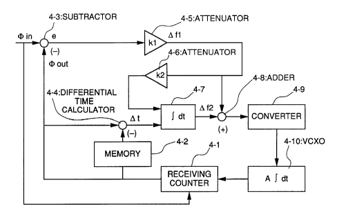
As shown in Fig. 1, the secondary type PLL according to the first
embodiment of the present invention is a standard clock transfer system
which, at a transmitting side , reads out counted values of the standard clock
at a random time intervals less than a time interval of T and transfers the
time information obtained at the transmitting side . This PLL device
comprises a receiving counter 4-1, which has the same structure as that of
the counter at the transmitting side , for counting the standard clock
received
by the receiving side; a memory 4-2 for storing an output of the receiving
counter for a predetermined period; a subtractor 4-3 for comparing between a
counted value of the receiving counter 4-1 and the received count value by
reading out the counted value of the receiving counter 4-1 whenever the
counted value of the counter of the transmitting side is transmitted; a
differential time calculator 4-4 for calculating the differential time between
the present count value and a preceding count value of the receiving counter
4-1; a first attenuator 4-5 for attenuating the output gain of the subtractor
4-
3; a second attenuator 4-6 for further attenuating the output of the first
attenuator 4-5; an integrator 4-7 for integrating an output of the second
attenuator 4-6 based on the differential time obtained by the differential
calculator 4-4; an adder for adding an output of the first attenutor 4-5 to an
output of the integrator 4-7; a converter 4-9 for converting the added value
of
the adder 4-9 into a voltage signal; and a voltage control oscillator 4-10 for
CA 02256583 1998-12-18
9
inputting the voltage signal converted by the converter 4-9 and for outputting
to the receiving counter 4-1.
Fig. 3 shows a construction of the integrator 4-7.
The transfer characteristic of the integrator is expressed by the
following equation.
Y (S) = 1/ S (7)
When it is extended on the Z plane, the characteristic can be rewritten
as,
Y (Z) = D t / 1- Zu (8)
The secondary type PLL is capable of operating such that the delay
element performs corresponding to D t for the random time information by
using 0 t as an operator for the integrator 4-7 by calculating 0 t from the
time
difference between the present count T(i) and the preceding count T(i-1).
As hereinabove described, the present invention is effective in providing
a PLL device having a fixed fitter suppression characteristic, by using
0 t obtained from the difference between the present count value T(i) and the
preceding count value T(i-1) as the operator for each constituting element for
enabling the delay element to operate coping with random time information.