Note: Descriptions are shown in the official language in which they were submitted.
CA 02256866 2002-09-26
1
COMMUNICATION SPEED SWTTCHING DEVICE
BACKGROUND OF THE INVENTION
Field of the Invention
The present invention relates to a device for
switching communication speed in a modem.
Description of the Related Art
In a facsimile protocol such as V.17 and V.29 in the
recommendation T.30, a calling side first transmits
Digital Identification Signal ("DIS") signal, Digital
Command Signal ("DCS") signal and so on at a low speed of
300bps, next transmits Training Check ("TCF") signal, an
image signal ("PIX") at a high speed, then transmits End
of Procedures ("EOP") signal again at a low speed.
In the latter half of the image signal PIX Return To
Call("RTC") signal is added. Tn the above recommendation,
the RTC signal is intended to be detected in an answering
side. When the answez-ing side detects the RTC signal, the
answering side shafts an apparatus mode from a high speed
signal reception mode to a low speed signal reception
mode, which enables t:he arnswering side to receive the EOP
signal that is a low speed signal coming next.
However the RTC signal is hard to recognize because
the generation tame is short. And it sometimes occurs
that the RTC signal cannot be detected when a switching
device is momentaril~~ interrupted by impulse noise and so
on, because the noise resistance of the RTC signal is
low. In this case, the low speed is received at the high
speed signal reception mode, which remains the problem
that the low speed signals after the EOP signal
CA 02256866 1998-12-22
2
can not be received.
SUMMARY OF THE INVENTION
It is an object of the present invention is to
provide a communication speed switching device capable
of shifting assuredly from a high speed signal reception
mode to a low speed signal reception mode.
The object is achieved by a communication speed
switching comprising a detecting section for detecting
a first frequency used in a low speed reception mode,
and a reception mode switching section for switching the
mode to the low speed reception mode when the detecting
section detects the first frequency for a predetermined
interval.
BRIEF DESCRIPTION OF THE DRAWINGS
FIG.l is a sequence diagram illustrating a
facsimile protocol in the recommendation T.30;
FIG.2 is a diagram illustrating the spectrum of a
high signal;
FIG.3 is a diagram illustrating the spectrum of a
low speed signal;
FIG.4 is a block diagram illustrating a schematic
configuration of a communication speed switching device
in the first embodiment of the present invention;
FIG.5 is a flow chart illustrating an operation of
the communication speed switching device in the above
embodiment;
FIG.6 is a diagram illustrating a signal point
CA 02256866 1998-12-22
3
arrangement on the complex plane;
FIG.7 is a diagram illustrating a signal point
arrangement on the complex plane in the above embodiment;
FIG.8 is a block diagram illustrating a schematic
configuration of a communication speed switching device
in the second embodiment of the present invention; and
FIG.9 is a flow chart illustrating an operation of
the communication speed switching device.
DETAILED DESCRIPTION OF THE
PREFERRED EMBODIMENTS
A communication speed switching device of the
present invention comprises a detecting section for
detecting a first frequency used in a low speed reception
mode, and a reception mode switching section for
switching the mode to the low speed reception mode when
the detecting section detects the first frequency for
a certain interval.
In the above constitution, it is possible to
acquire the timing of switching a mode to a low speed
signal reception mode by other signals except the RTC
signal . That makes it possible to detect a signal coming
after the RTC signal when the RTC signal can not be
detected so as to achieve the reliable communication.
It is preferable that the communication speed
switching device comprises a first deciding section to
decide, when the detecting section detects a signal of
a first frequency for a predetermined interval, that the
..... ....u..~. ~......_...~..~.W.~,....~._.~~.w __._ .........._.~...
CA 02256866 1998-12-22
4
detected signal is a low speed signal. In this manner,
it is possible to recognize a low speed signal indicative
of protocol end and so on, which enables the apparatus
to shift to the low speed mode assuredly after at the
time of the protocol end.
In the communication speed switching device, it is
preferable that the first deciding section decides, when
the first deciding section detects a signal of a second
frequency used in a high speed reception mode, that the
detected signal is not a low speed signal. In this
manner, it is possible to recognize the mode is still
in the high speed reception mode in spite of receiving
a low speed signal, and continue receiving a high speed
signal such as image signal. As a result, it is possible
to prevent the change of the mode as receiving the image
signal and so on.
In the above communication speed switching device,
it is preferable that the detecting section decides that
a signal of the first frequency is detected when the
energy of the detected (first frequency) signal exceeds
the predetermined level. In this case, it is preferable
that the detecting section detects a signal of a
frequency around the first frequency that has the energy
exceeding the predetermined energy level.
In some signal patterns, the signal of the
frequency around the first frequency has higher energy
than the signal of the first frequency. By the
CA 02256866 1998-12-22
constitution, even in such case, it is possible to
recognize a low speed signal and shift to a low speed
reception mode assuredly.
In the communication speed switching device of the
5 present invention, it is preferable that the detecting
section comprises a second deciding section for deciding
whether or not the energy level of a demodulated signal
is within a predetermined level. In this manner, it is
possible to easily recognize a low speed signal by
deciding whether or not the energy level is within the
predetermined level, because, for instance, a low speed
signal that is not QAM modulated indicates a certain
energy level after QAM demodulated.
In the communication speed switching device, it is
preferable that the second deciding section decides that
a received demodulated signal is not a low speed signal
when the energy level of the received demodulated signal
is out of the predetermined level. In this manner, it
is possible to recognize the mode is still in the high
speed reception mode in spite of receiving a low speed
signal, and continue receiving a high speed signal such
as image signal. As a result, it is possible to prevent
the change of the mode as receiving the image signal and
so on. In the communication speed switching device, it
is preferable that the predetermined level is indicated
in a signal point arrangement diagram in the complex
plane.
CA 02256866 2002-09-26
6
It is preferable that the communication speed
switching device comprise a third deciding section for
counting a signal of the first frequency and deciding
that the signals are low speed signals when the
predetermined number of the signals are counted. In
this manner, it is possible to recognize a patterned
instruction signal indicative of a Low speed reception
mode shift, which allows the response to various
instruction signals for the low speed reception mode
shift from a calling side. As a result, it is possi ble
to perform the reliable shift to the :Low speed reception
mode using the patterned signal.
Hereinafter, the embodiments of the present
invention are explained in detail with reference to the
attached drawings.
FIG. 1 is a sequence diagram to explain V.17 and'T.29
facsimile protocols in T.30. In =(nose protocols, as
described above, DTS signal f rom an answering side and
DCS signal from a calling side are communicated at a low
communication speed, next TCF signal and PTX signal from
the calling side are communicated at a high communication
speed, then EOP signal and Message Confirmation ("MCF")
signal are communicated at the low communication speed.
As described above, the above protocols include Low
speed signal communication and high speed signal
communication. In the high speed signal communicat-on,
for instance, as illustrated in FIG.2, signals of 500Hz
CA 02256866 2002-09-26
7
up to 2900Hz are transmitted and received in accordance
with V.29 recommendation. In the low speed signal
communication, for instance, as illustrated in FIG.3,
two signals of 1650Hz and 1850Hz. In addition, each of
the two signal indicates "0" and "1" . In other words,
signals in the high speed signal communication are
composed of a plurality of signals at the band of 500Hz
up to 2900Hz, and signals in the low speed signal
communication are composed of only two signals of 1650Hz
and 1850Hz.
In the present invention, low speed signals are detected
utilizing the characteristics of those signals. In addition, in
the present specification, the low speed signals to be recognized
mean EOP signal, End of Message ("EOM") signal and Multi-Page
Signal ("MPS") signal in accordance with T.30 recommendation.
Hereinafter, the embodiments of the present
invention are explained with reference to the attached
drawings.
(First Embodiment)
In the embodiments of the present invention, an
explanation is given to the case of switching a mode from
a high speed reception mode to a low speed reception mode
by recognizing the low speed signal when obtained a
predetermined energy of at least one of signals at 1650Hz,
~.750Hz and 1850H~ which are signals in a low speed signal
communication for a predetermined interval.
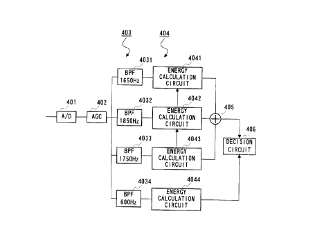
FIG.4 is a block diagram illustrating a schematic
CA 02256866 1998-12-22
8
configuration of a communication speed switching device
in the first embodiment of the present invention. The
communication speed switching device is applied in a
modem in a data communication apparatus, for instance,
facsimile apparatus. The communication speedswitching
device comprises A/D converting section 401 for
converting an analogue signal into a digital signal, AGC
section 402 for performing the automatic gain control
of the converted digital signal, band pass filter 403
for detectingeachfrequency, energycalculating circuit
404 for calculating energy of each frequency, adding
section 405 for adding a signal of each frequency and
decision circuit 406 for deciding each frequency.
Band pass filter 403 includes filter 4031 for a
signal of the frequency at 1650Hz, filter 4032 for a
signal of the frequency at 1850Hz, filter 4033 for a
signal of the frequency at 1750hz, which frequencies are
used in a low speed signal communication, and filter 4034
for a signal of the frequency at 600Hz used in a high
speed signal communication.
And energy calculating circuit 404 includes
calculation circuit 4041 a signal of the frequency at
1650Hz, calculation circuit 4042 for a signal of the
frequency at 1850Hz, filter 4043 for a signal of the
frequency at 1750hz, and calculation circuit 4044 for
a signal of the frequency at 600Hz each corresponding
to filters 4031 up to 4034 respectively.
CA 02256866 1998-12-22
9
And decision circuit 406 comprises a timer (not
shown) for counting a time receiving a signal of a
frequency used in a low speed signal communication.
Next the communication speed switching device with
the above configuration is explained using a flow chart
illustrated in FIG.5. In step (hereinafter abbreviated
as S) 501, a modem starts up and a facsimile communication
starts. In S502, it is decided whether or not the
reception is performed with respect to at least one of
a signal of 1650Hz passed through band pass filter (BPF)
4031 and processed for the energy calculation in
calculation circuit 4041, a signal of 1750Hz passed
through band pass filter (BPF) 4032 and processed for
the energy calculation in calculation circuit 4042, and
a signal of 1850Hz passed through band pass filter (BPF)
4033 and processed for the energy calculation in
calculation circuit 4043. In other words, either is
preferable to examine the reception of each signal of
1650Hz, 1750Hz or 1850Hz or to examine the reception of
added signals of 1650Hz, 1750Hz and 1850Hz.
In this embodiment, it is intended that a signal
of 1750Hz is detected along with signals of 1650Hz and
1850Hz that are used in the low speed reception mode.
It is because that a signal of 1750Hz generated higher
than a signal of 1650Hz or a signal of 1750Hz when a bit
pattern of "0101" of V.21 signal at 300bps that is the
low speed is transmitted. Therefore by detecting the
CA 02256866 1998-12-22
signal of 1750Hz, in other words, detecting a signal of
a frequency around 1650Hz or 1850Hz along with signals
of 1650Hz and 1850Hz, it is possible to perform the
reliable detection of the low speed signal assuredly.
5 Accordingly, in such case, it is possible to switch a
mode to the low speed reception mode assuredly.
Each low speed signal processed for the energy
calculation in each of energy calculation circuit 4041
up to 4043 is added in adding section 405. At this time,
10 a timer starts in decision circuit 406.
On the other hand, it is decided in S503 whether
or not the reception is performed with respect to a signal
of 600Hz (second frequency) that passes through band pass
filter 4034 and has the predetermined energy calculated
in energy calculation circuit 4044. Since a sianal of
600Hz is a signal used in a high speed reception mode,
specifically which is included in signals of 500Hz up
to 2900Hz generated in a high speed image signal mode
in accordance with V.29 and comes during high speed
signals are continued, it is decided that the high speed
reception is continued when the signal is received. In
other words, it is decided that the signal is not EOP
signal that comes after PIX signal. In this case, in
S504, the timer in decision circuit 406 is reset. And
the above operation is repeated.
In this manner, it is possible to recognize that
the high speed reception mode is continued however low
CA 02256866 1998-12-22
11
speed signals are received, which makes it possible to
continue receiving high speed signals such as image
signals. That can prevent the change of the reception
mode during receiving, for instance image signals.
Next in 5505 up to S507, when the timer in decision
circuit 406 obtains a predetermined time and the energy
level of signals of 1650Hz, 1750Hz and 1850Hz reaches
a predetermined gain level, it is decided in decision
circuit 406 that signals of 1650Hz, 1750Hz and 1850Hz
that are low speed signals are detected, and recognized
that the signals are EOP signals that come after PIX
signal. In this manner, the modem detects the low speed
signals. Accordingly, a facsimile apparatus controls
the shift to a low speed signal reception mode based on
the indication that the modem detects the low speed
signals.
Thus, by always detecting a signal of 1650 Hz and
a signal of 1850Hz after the modem starts up, it is
possible to recognize the low speed signals. That
allows the detection of the low speed signals, the
reliable switching to the low speed reception mode and
the reliable communication in the case of not detecting
a signal indicative of instruction of switching from high
speed signal to low speed signal such as RTC signal.
In addition, in this embodiment, the case is
explained where EOP signal is recognized when the signal
energy level at a predetermined interval exceeds a
CA 02256866 1998-12-22
12
predetermined level. However, it is preferable to
control the shift from the high speed reception mode to
the low speed reception mode by deciding EOP signal when
"01111110" (7E) is recognized. "0" is counted when a
signal of 1850Hz is detected for 3.33msec, and "1" is
counted when a signal of 1650Hz is detected for 3.33msec.
"01111110" is recognized by counting first "0", next six
of "1" and further "0".
That is, in this embodiment, it is possible to
recognize a patterned instruction signal indicative of
the low speed reception mode shift, which allows the
response to various instruction signals for the low speed
reception mode shift from a calling side. Thus it is
possible to perform the shift to the low speed reception
mode assuredly using a patterned signal.
(Second Embodiment)
In this embodiment, the attention is paid to that
a transmitted low speed signal that is not processed for
QAM (Quadrature Amplitude Modulation) modulation
indicates a certain energy when processed for QAM
demodulation. An explanation is given to the case of
recognizing EOP signal when the QAM demodulated signal
indicates a certain energy level, then switching from
a high speed reception mode to a low speed reception mode.
In this embodiment, specifically, a signal point
arrangement diagram in the complex plane when low speed
signals are received in the high speed signal reception
CA 02256866 1998-12-22
13
mode is recognized to utilize. Hereinafter, the
principle is explained.
FIG.6 illustrated a signal point arrangement
diagram (pattern) when receiving signals of 9600bps, and
FIG.7 illustrated a signal point arrangement diagram
(pattern) when receivingsignals of 300bps,inaccordance
with V.29 recommendation. Ordinary, a high speedsignal
is QAM modulated, and is demodulated at an answering side
by QAM demodulation.
When it is assumed that a single frequency signal
is cosc~ t(c~ :1650Hz or 1850Hz) , a carrier frequency for
QAM demodulation is co Orad/f ( 1700Hz in V.29) , a real side
(R) of a QAM demodulated single frequency signal is
expressed as below.
R=COSCJ t ~cosc~0 t =(cos(co+c~0) t +cos(c~-c~0) t )/2
Eliminating cos ( ~ -f- cu 0) t that is a high frequency side
introduces cos ( cu - w 0) t / 2 . On the other hand, an
imaginary side ( I ) of the signal is expressed as below.
I =cosco t ~sinco0 t =(sin(c~+co0) t -sin(co-coo) t )/2
Eliminating sin ( cu -~ c~ 0) t that is a high frequency side
introduces - sin ( c~ - cu 0 ) t / 2 .
The square of a length from the original point in
pattern is expressed as below.
R2+ I2=cos2(c~-~0) t/4+sin2(c~-~0) t/4=1/4
It is understood that the above equation indicates a
certain value not depending on the frequency.
Accordingly, when signals that are not processed
CA 02256866 1998-12-22
14
for QAM modulation have a certain energy after they are
QAM demodulated and make a circle in the eye pattern as
illustrated in FIG.7. Thus, the eye pattern is used to
recognize receiving a low speed signal that is not
processed for QAM modulation. This principle is used
to detect a low speed signal.
FIG.8 is a block diagram illustrating a schematic
configuration of a communication speed switching device
in the second embodiment of the present invention. The
communication speed switching device comprises QAM
demodulation section 801 for inputting sincot and
cosc~t for QAM demodulation to multiply by input data,
calculating section for calculating a scale of gain of
the eye pattern of the QAM demodulated data, and deciding
section 803 for deciding a calculation result in
calculating section 802.
FIG.9 is a flow chart to explain an operation in
a communication speed switching device configured
described above. A modem starts up in 5901, and (X, Y)
in the complex plane is always detected in S902.
It is decided whether or not a value of ~ ( X ~-+- Y ~) is not less
than 4 (d~ (X~-f-Y~) >-_4) in S903, and it is decided whether
or not the value of ,;r ( X ~-~ Y =) is more than 3 ( J'~ ( X ~+ Y')
~3) in 5904. These decisions are to examine whether or
not the value indicates a predetermined energy level in
the signal point arrangement diagram. Accordingly,
when the energy level of a low speed signal that is not
CA 02256866 1998-12-22
QAM modulated indicates, for instance, 3.674 after the
signal is QAM demodulated, NO is decided both in S903
and S904.
And in S905 and S906, when this state in the eye
5 pattern lasts for a predetermined interval, the signals
are identified as EOP signal. Then the mode is shifted
from a high speed reception mode to a low speed reception
mode.
Thus, when low speed signals are received in the
10 high speed reception mode, since the energy level in the
detected eye pattern indicates a predetermined level,
it is easy to identify low speed signals. It is thereby
possible to recognize the detection of low speed signals,
which allows the reliable communication.
15 In addition, in this embodiment in the same way as
the first embodiment, by deciding that a demodulated
signal is not EOP signal when the energy level of the
demodulated signal is out of the predetermined range,
it is possible to continue receiving high speed signals
such as image signals. That prevents the change of the
reception mode while receiving image signals and so on.
In the above embodiment, the explanation is given
to the case where it is assumed that RTC signal, which
is installed in the latter half of PIX signal, is not
received. However, the present invention is not limited
by the above case, and is applicable to any case of
switching a high speed signal to a low speed signal. And
CA 02256866 1998-12-22
16
in the present invention, it is preferable to change
frequencies or a predetermined level properly to
practice, not being limited by the numbers or values in
the embodiments.
In the above embodiments, the explanation is given
to the case where a low speed signal to identify is EOP
signal. However, the present invention is applicable
to the case where the low speed signal is EOM signal or
MPS signal in the same way.
In the above embodiments, the explanation is given
to the case where the communication speed switching
device is applied to a facsimile apparatus. However,
the communication speed switching device of the present
invention is applicable to other data transmission
apparatus.
As described above, in the communication speed
switching device of the present invention, by
recognizing a specific pattern of a signal point
arrangement obtained when detected first appearing
signals of a specific frequency as a low speed signal
(EOP signal) or detected low speed signals, it is
recognize the timing of switching high speed signals to
low speed signals. Thereby it is possible to perform
a reliable communication by shifting a mode from a high
speed signal reception mode to a low speed signal
reception mode.