Note: Descriptions are shown in the official language in which they were submitted.
CA 022~93~6 1998-12-24
Applicant Firm:MM-~esastift Manager Mem-~y GmtH
Draifaltigkaitskergstrasse 44
C-7~54~ Spaichingen
DA~A AC~IJISI~ION DEVICE FOR OP~ICA~IY AC2lJIRING AND S~ORING
VISlJA~Y MARKED AND PRO~EC~ED A~HANIJM~RICA~
CHARAC~ERS, C-RADHICS AND eHO~C-RA~HIC ~IC~IJRE AND/ OR ~HREE-
~IMENSIONA~ ~OPOGRA~HIES
A scanner fcr the electrcnic ac~uisition and storage Gf
alphanumerical characters is already knGwn from document
~O 32/11~10. ~ith su_h devices, the light of a radiation source
is prcjectad via a projêcticn davicê ontG a predetermina~le cletail
of a surface marked wi~h alphanumêrical characters and the
reflected light is reprGdu~ed via an optical unit cn an image
sensor converting the light into a se~uence of electrcnic signals.
A motion detector registers at the same time the motion of the
scanner along a line ~f characters. A signal processing
electrGnics integrated in the data acquisition device c_nverts the
signals int~ a sequence cf characters each corresp~nding with
alphanumerical sym~~ls. ~he chara~ters can ~e stored as
alphanumerical sym~_ls in an integrated memory or transmitted via
an interface to a csmputer fcr further processing.
Such scanners ara limited tc ac~uiring and st~ring
alphanumerical characters line ~y line ~u~ ar~ n~t capa~le Gf
ac~uiring graphic reprêsêntations ~r phctographic pictures.
CA 022~93~6 1998-12-24
~ urthermore, a hand-h~ld s_anner in the form of a reading
pen f_r reading in characters is kn_wn fr~m internati-nal
apFlicati~n WO 94/00825. ~-r this purp~sc, the reading pen is
m~ved line-by-line acrcss lines ~f characters. In this process,
at least part of the line is illuminatad and the reflected light
is captured and convertsd into digital informaticn, only
infcrmaticn representing a character cr the end cf a character
being recorded. ~his informaticn is subsequently supplicd to a
character recogniti_n devica and finally stcred, e.g. in an ASCII
text file.
~ his hand-h21d s~anner has the drawba~k that it is pGssible
cnly to read-in characters corresponding with the preset
recognition pattern. Reading-in pictured information not
structured alphanumerically is nct pcssible.
A hand-held copying device that becama kncwn earlier from
~uropean patent application ~e 0 278 004 does not have the above
drawback. ~his device first picks up the entire information
availakle in the plane cf a picture and files it almcst
unprocessed in a matrix data mam-ry.
Hcwever, this device, toc, is designed only for time-
oriented data acquisiticn. ~his has the drawback that a text
arranged, for example, in a curve can be acquired ~nly by
gathering a substantially quadrangular detail ccvering the entire
region cf the curve, which means that an amount of data not of
interest for the predcminating part is always jcintly acquired and
.,. ,. . .. ~
CA 022~93~6 1998-12-24
filgd .
~ herefore, the inventi~n is bassd on the problem cf creating
a data acquisiti~n device permitting mem3ry--ptimized acquisition
of any desired infcrmation available in the plane of a pictura
free of any direction _f mcticn preset f-r such acquisition.
~ his problem is s-lved by a data acquisiti3n device with the
features of claim 1 -r claim 26.
~ When employed as intsnded, the data acquisition device as
defined by the inventi~n acquires in an optical manner a freely
selectable part of an image plane marked with alphanumerical
characters, graphics or Fh_tographic images, and converts the
-ptical signals int- a sequence _f electr-nic signals, which are
stored in a manner accessible to further electrcnic processing
with retentiGn -f the complete -riginal pictured infGrmatiGn, and
which can be recalled. ~n "OCR" (Optical Character RecGgnition)
text search software thus can ke dispensed with.
Illumination usefully sh~uld take place with mGnochrome
light in Grder tc avcid dist~rtiGn of the cptical acquisition due
to dispersion. Infrared light is particularly suitable in this
cGnnection because it has greater depth cf pen=tratiGn than
visible light Gn mark2d surfac3s usually employ2d such as, fGr
example, white paper, sc that it permits distinguishing the
infGrmation to be acquired from impurities.
, . , . ... .. ~ , ...
CA 022~93~6 1998-12-24
S~ as t~ allcw variable adjustment _f the image plane
section or segment tc be acquired, it is useful if a projection
device having a shutter with a variable aperture is mounted cn the
data acquisiticn device. Particularly suitable fcr this purpose is
a slotted shutter whose slot size is infinitely variable and
permits acquisition ~f a beam-like detail.
In the interest of a simple structure of the data
acquisiti-n device provisi-n is made acc_rding to a useful further
development of the invention that the radiation source is
integrated in the image sensor, so that the light cf said source
is guided thr_ugh the same optical channel as the reflected light.
~ articularly simple handling is obtained if the motion
detector is connected with the data acquisition device in a fixed
manner, and if said detect~r has a s-anning elem_nt which is
designed rotatiGn-symmetric and which is arranged Gn the mGtion
detect_r in such a way that it is rctatable about at least Gne
axis as well as guidakle along the area to ba acquired.
Detection of the m~vement cf the data acquisition device on
the section usefully can take place with the help of the
Hall-effect. ~o this extent, provision is mada aocording tG
another impGrtant furthar develGpment of tha invanticn that the
moti_n detector has a Hall-element with a s~anning element,
whereby the scanning element is surrcunded by an inhcmcgenecus
CA 022~93~6 1998-12-24
magnetic field. ~he r~tary mcticn of the scanning element causes
a peri~~ hang2 in the Hall-v~ltaga induc3d in th2 Hall-alem2nt
Said affect parmits ths detsrminaticn cf the p~SitiGn of the data
acquisition device ~n the secti_n.
According to ancther further devel~pment the scanning
element c_nsists of a sphere supp~rted in a freely rctatable way
and having magne~ platelets arranged on its surface, such small
plates keing aqually spaced fr~m each cther. ~he movement of ths
data acquisiti_n device _n the se_ticn can be detected in this way
both in the h~rizontal and verti~al directi~ns.
In another emb~dim2nt, the data acquisiti~n device is
pr~vided with an electrcnic closure, through the actuation cf
which it is pcssikl2 t~ freely determin2 that part Gf the section
which is tc be filed by the signal processing unit in an
information packet.
For more rapid information processing it is possible tG
integrat2 the one cr mcre memcri2s intend2d fcr rec2iving the
infcrmaticn packets in the signal prccessing unit.
In yet ancther embodim-nt the signal pr~_essing unit may
have devic2s for ccnnecting external memcries. It is pcssible in
this way to stcre also compreh2nsiv2 texts or ccmplex pictured
dccuments.
~ he current uptake and the operating vcltag2 can be clearly
.. . .. .
CA 022~93~6 1998-12-24
reduced if the signal pr~cessing unit and the memory unit are
already integrated in tha imaga sansor.
For external furthar procassing of the data it is usaful if
the signal processing unit and/_r the memory unit of the data
acquisition devica are optically, alectronically or
~pt~electronically conne~ted to an interface for transmitting data
to external devices.
For easier handling, the data acquisiticn device should ke
equipped with a battery ~urrent supply whi_h usefully can be
oparated with rechargeable katterias. ~ha current infeed for
charging the katteries takes place either via a slide-in device
that is detachabla fr_m the data acquisition davica, or via a
cable connected to the interface. ~he process for charging the
batterias can ba optimized alsc by integrating a charging
ele~tronics prefarakly in tha c_mputsr intarfa~e card subjecting
the charging process t~ ccntinu~us electr~nic ~ontrol.
Furthermcre, advantage~us is als~ the p_ssikility ~f
continuously controlling th- acquired or stored data. Acccrding
~- a further emkodiment ~f the inventi~n, a m~nitor may serve for
this purpose, such monitor being contrclled by a signal processing
chip integrated in the signal prccessing unit. ~hus the acquired
image inf~rmation can be visually ~isplaye~ _nline. However~ it is
pcssible alsG t_ call in all inf_rmati-n packets which were filed
in the mem~ry unit and which are visikle as readable image
representation. ~he monitor can be designed in this c_nnaction
.. , . .. ~ ..
CA 022~93~6 1998-12-24
als~ as a slide-in unit which, when rsquired, can be ccnnected to
the data acquisiti~n device, or alsG can be separated from the
latter.
~ hs l_w space requiremants _f m~dern micr-electr_nics permit
the particularly useful emb_diment of the in~ention as a manual
device, f_r example in tha f~rm -f a f-untain Fen.
Acc~rding to yet another embodiment of the invention, the
characters, graphics or images to be acquired are marked with a
beam of visible light and a superimposed beam of infrared light
congruent with the former. ~he reflected light bundle is
decomposed into its visible and infrared components by a
semitransparent mirr_r, which is permeable -nly to infrared light,
wher~by -nlv the infrared light components are used for image
acqulsltlon .
Such infrared light image acquisition has the advantage that
it is still pcssible for the image ssns-r to process and utilize
even soiled or blurred characters. ~urthermore, the image sensor
is capable of acquiring also characters in the color of the
visible light used f~r the marking.
In an~ther embodiment, the data acquisition device has a
mcti~n detectcr permitting ccnta_t-free acquisiticn cf the
movement cf the data acquisiticn device parallel with the section.
~his is ,carticularly advantag32us if the sa_ti_n does not readily
CA 022~93~6 1998-12-24
permit detecticn cf mction, fcr exarr,ple by means of a scanning
sphere, fcr example in _ase cf a relief-like surface structure, cr
in _ase cf surfa~es whi_h are s_nsitive tc t~u~hing. ~pti~al
senscr devices can be ccnsidered in this ccnnecticn as
ccntact-free acquisiticn means; hcwever, cther pcssibilities are
conceivable as well, for example such as acquisition of the motion
ky rr,eans of scund waves cr magneti_ fialds.
AccGrding to claim 27, prcvisicn is rr,ade fcr photodiodes as
particularly advantagscus means fcr acquiring the mcticn, which
detect the light cf radiati_n scur-e reflected by the selected
se~ti~n. In this ccnne_ticn, the radiaticn s_ur_e may ke the cne
used alsc fcr rec~rding the image; hcwever, a separate radiatcr
for detecting the mcticn is con_eivable as well. During mcvement
cf the data acquisiticn device, the phctcdicdes are arranged in a
substantially parallel data a-quisiticn plane with regard tc the
selected secticn in such a way that due tc the time sequence of
the electric signals supplied by the phctcdicdes, it is possible
tc clearly allccate the mcvement perfcrmed by the data acquisiticn
device vis-a-vis the se~ticn. In crder tc detect in this manner
any mcticn parallel with a suLface it is necessary tc space the
phctodiodes in the plane in at least twc different directicns.
~he signals emitted by the phctcdicdes can be used at the same
time as reference signals in crder t~ carry ~ut a ~crrectiGn-
~crrlpensation, fcr example in crder tc assure line-ccrrect
acquisiticn cf texts.
CA 022~93~6 1998-12-24
~ he motion detactor advantageously has maans for datecting
the vertical spa~ing cf the data acquisiticn davica fr_m the
selactad saction. ~he vertical spacing is praferably measured in
tha cptical or infraredùcptical manner, for example by means of
cna Gr a plurality ~f ph-t_di-das which data_t tha light raflected
by tha saction. In this casa, tG_, provisicn can ba mada for a
saFarator radiator fcr measuring tha vertical spacing; however, it
is conceivable also to empl_y for this purpose the radiation
source used for detecting the motion and/or for the recording of
the image
In the furthar davalcpad amk-diment acc_rding tc claim 29,
it is no longar raquirad to maintain the data acquisition davica
at a constant spa~ing ralativa t_ tha secti~n. In this furthar
developed embodiment, tha f-cal langth -f the focusing unit is
adjustad in dependenca upon vertical spacing of the data
acquisition davice frcm the sale~ted sactiGn - said vartical
spacing baing datacted by a suitabla maasuring instrument - in a
way such that tha selacted saction is always reproduced on tha
image sensor at any vertical spa-ing.
In another advantagecus further developed embodiment the
radiation sour~a employed for the detaction of tha motion and/or
the vartical spa~in3 is intagrated in the moti-n detactor. A
semiconductor radiator is preferably amployad as such a radiation
sourca, which is favorable in terms of manufacturing cost and
which is saving space and energy when used.
CA 022~93~6 1998-12-24
In y3t anothar advantagesus further developed embodiment,
th2 maans f_r d2t2cti~n the mcvement and/~r the means fGr
det2cting ths v2rtical spacin~ and/-~r the radiati_n source, for
example a semiconductcr radiatcr, are integrated in a microchip,
which is arranged in the mcticn det2ctcr.
According t~ claim 32, the signals emitt2d by the means for
detection of the mct-ion and/cr the m2ans for det2cting the
vertical spacing are c_nverted int~ digital synchronizing signals,
which are stored in the memory of th2 data acquisition device
together with the inf~rmati~n packet ~f the simultanecusly
rec~rd2d imag2 inf~rmation. In this way, true-t_-scale and
correct reproduction of the pictured information is possible also
when transmitting the data t_ an axt2rnal device such as, for
example a PC.
In a furth2r dev21cp2d emk~diment acccrding tc claim 33, the
data acquisiticn devic2 is suitable fcr acquiring
thre2-dimensional infcrmaticn. ~-r this purpsse, the image s2nsor
has suitable means permitting detection of a thre2-dimensional
character of objects. Such means may be cf, fcr example the
sterecscopic or hclcgraphic type.
As a particularly advantagecus means fcr detecting the
three-dimensional character cf objects, prcvisi_n is made
acccrding tc claim 34 f_r an image s2nscr having twc detectcr
CA 022~93~6 1998-12-24
matrices which ea_h are sensitive cnly in a spectral secticn of
the frequency spe_trum emitted by the radiati~n s~urce ~f the
cptical unit of the data acquisiti~n devi-e, namely in a way such
that the two secticns do not overlap each other cpectrally. For
three-dimensional dete~ti_n, the tw_ dete-t_r matri_es are
contrGlled shifted in time, for example by means of a bistable
switch, and the different image inf_rmati~n _f the tw_ detector
matrices is converted in a suitable data processing device into
informaticn about the three-dimensional structure of the section
In ancther further developed emk-diment, the data
acquisition device a--~rding t_ claim 35 has a transmitting and
receiving unit, ky means _f whi-h wireless communicatiGn is
possible with an external c~mputer.
So that als~ handwritten inf~rmaticn can be converted into
~D~-readable informati~n, the signal pr~-essing unit is exchanging
data with a memory medium containing corresponding reference
information. F~r example, hand-written inf_rmati~n can be filed
in this way in the image memory as standardized hexadecimal code
characters.
In yet another advantage~us further devel~ped emb~diment,
the data acquisiticn device is pr~vided with an input unit, f_r
example a keyb~ard, by means ~f which it is p~ssikle t~ ~all up Gr
input informati~n ab_ut selectable prccessing pr_grams such as
text, chart or graphic programs.
CA 022~93~6 1998-12-24
In another advantageous embodiment, the data acquisition
device consists ~f at least tw_ separate and functicnally
autonomcus units. ~ne data acquisiticn unit sarves for acquiring
the information contained in ths selscted section. By means of
preferably remote wireless data transmission said informaticn is
transmitted to a pr-cessing unit ky means of which the read-in
data are processad. ~he procassing unit in turn may be divided in
functionally autonGm~us units, for example a control unit and an
indicating unit. Su-h a design facilitates handling of the data
acquisition devi_e. In parti_ular, the reading unit can be
designed in the f_rm Gf a small-v~lume and lightweight data
acquisition device owing to the fa-t that it is possible to
dispanse with the installati_n of data processing hardware and the
c-oling systems etc. necessarily ~cnne~ted therewith.
~ he control unit of the aforementl~ned data acquisition
device is usefully provided with sensor means for the input of
contrcl ccmmands ~r other inf~rmati~n. Using a so-called touch
pen it is possible in this way t_ empl-y the data acquisition
d_vica as a keybsardless p~cket ~C. As t~u_h pens it is possible
to ccnsider, f-r example a c-rresp_ndingly designed read-in unit.
In a further developed emb_diment, the read-in unit is
designed at the sam- time as a writing t_~l and permits the
processing of inf~rmati~n previcusly written ky hand with the
read-in means.
. . . ~ . . .
CA 022~93~6 1998-12-24
Fcr explaining the inventicn in greater detail, an
exemplified emkodiment is described in the f-ll-wing by reference
to the attached drawings sh-wing the f-ll-wing by schematic
representations:
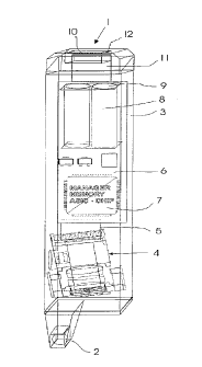
FIG. 1 sh~ws the structure _f a data acquisiti-n davica
designed in ths f-rm cf a hand-held device, with a m_tion
detector, an optics, a signal processing unit, an integrated
battery supply unit, and an integrated interface.
FIG. 2 shows a view of data ac~uisition davica 1 when used
as intended.
FIG. 3 sh-ws a l-ngitudinal secti_n thr-ugh the optics of
the data acquisiticn device ccnsisting cf an image sensor, a
focusing unit and a slotted shutter.
FIG. 4 is a top vieW of the sl~tted shutter of the
-ptics.
FIG. 5 is a general sketch explaining the so-called
Hall-effect.
FIG. 6 shows a secticnal view of the structure of a moticn
detectcr designed as a Hall-generator.
FIG. 7 is a parspective vieW of the motion detector designed
CA 022~93~6 l998-l2-24
as a Hall-generat~r unit.
FIG. ~ is a side vieW ~f tha m-ti-n detect-r.
FIG. 9 shGws the schematic structure cf tha data acquisition
d2vi~s in a blo-k diagram.
FIG. 10 sh~ws with tha halp _f a kl~ck diagram th~ read-in
and stcring of informaticn by maans of tha data acquisition
device.
FIG. 11 shows with the halp of a ganeral sketch the
transmission ~f ths data acquirad ky tha data acquisition device
tc an electronic data processing installation.
FIG. 12 is a parspactiva viaW _f a data acquisition davica
with a monitor davised as a slide-in unit in its ~perating
condition.
FIC-. 13 is a parspactive vieW ~f tha m_nit_r slida-in unit
by itself.
FIG. 14 also is a ,cerspactiva viaW of tha data acquisition
devica according t~ FIG. 12 with the m~nitor slida-in unit in its
nonoperating condition.
FIG. 15 sh_ws by a lcngitudinally sectional view like in
~ ... . . . .
CA 022~93~6 l998-l2-24
~IG. 3 an optics with a red-light radiatcr, an infrared light
radiat~r, and a ssmitranspar3nt mirror arranged in the path cf the
light keam.
FIG. 16 shcws the ~pti_es represented in ~IG. 15; hcwever,
with the path ~f the light refla~ted by the sale-ted secticn.
~ IG. 17 shows tha structure ~f a data acquisition device of
ancther design with a c_nta_t-free mcticn detectcr, an adjustable
fccusing cptics, as well as with an input unit.
~ IG. 18 shcws a lcngitudinal secticn thrcugh the ccntact
free mction dete-tor represented in ~IG. 17.
~ IG. 19 shows the mode cf cperaticn cf the detecting means
cf the mcticn dete_tor sh~wn in ~IG. 18 by block representations.
FIG. 20 shows a bl~-k diagram f~r explaining the mode of
operation of the motion detector represented in ~IGS. 17 and 18;
and
~ IG. 21 is a bl~ck diagram fcr explaining the m~de Gf
operation of an image sensor for dete~ting three-dimensional
obje~ts.
~ IGS. 22 to 24 show a data acquisiticn device of ancther
design, where the devices for reading in-, contrGlling and
CA 022~93~6 l998-l2-24
indicating each are designed as separate units exchanging data
with ea~h ~ther, whereby:
FIG. 22 is a read-in unit;
FIG. 23 is a ccntrcl unit; and
FIG. 24 is an indicating unit of such a data acquisition
device.
~ he data acquisiticn device 1 sh~wn in FIG. 1 csmprises a
moticn detector 2 sclidly jcined with said data acquisition
device, said mcticn dete~tcr pr~jê~ting fr_m a hcusing 3 designêd
as a handle. Integrated in hcusing 3 are an cptics 4 serving fcr
image acquisiticn, a bsard 6 c~nnected ts cptics 4 via a multi-
ccre ccnnection cable 5, with a signal processing unit 7 and a
battery supp~y unit 8 with chargeable batteries 9 being arranged
on said board; furthermore, an interface 10, which is
electrcnically ccnnected t~ bcard 6 via a ccnnecticn cable 11; and
an interface card 12.
optics 4, which serves fcr image a~quisiticn, ccnsists cf a
CCD image senscr 14, which ccnverts cptical image signals intc
electrcnic image signals, and in which a semiccnductcr radiatcr 17
is integrated, said radiat~r ~adiating, f~r example greên light.
A prcjecticn devi_e lc with an cpti_al fccusing unit 18 is
arranged cn image senscr 14. Fccusing unit 18 c_nsists cf cne
l6
CA 022~93~6 l998-l2-24
~iconvsx, one planocon~ave and one ki_oncave lens, as well as of a
slotted shutter 16, whi-h is arranged on the side of projection
device 15. when the data a-quisition devi_e is emplcyed as
intended, said projection device is fa~ed by the information
carrier carrying the information tc be a_quired. Slctted shutter
15 has two lamellae 23, 23', which form a slot 24 which is
variably adjustable via a rctatakle adjustment ring 25. For
adjusting the slot, the slot lamellae 23, 23', which are guided in
the radial directicn alcng tw- guide rails 2~ arranged on a
cir-ular disk 27 c-nne-ted in a fixed way with pr-je_tion device
15, each are pressed by a radially ~utwardly dire-ted force of a
spring 29, 29' joined fixed with guide rails 2~ against an
elliptic framing 26 ccnnected fixe~ with adjustment ring 25.
~llipti_ framing 26 is designed in this -_nnecti_n in such a way
that sl-t 24 is __mpletely _l-sed when the lamellae 23, 23' are
arranged with their guiding device parallel with the small
semi-axis of the ellipse formed by framing 26. A rotation cf
adjustment ring 25 causes the slot lamellae 23, 23' to bê forced
apart, enlarging the slct 24. A maximal sl~t size is reached with
an adjustment in which the lamellae 23, 23' are arranged with
their directicn cf guidance parallel with the large semi-axis cf
the ellipse fcrmed by the framing 26.
Due tc the cooperaticn of f~-using unit 1~ with slotted
shutter 16 it is pcssible to illuminate with the light of
semiccnductor 17 a freely selectable secti~n 13 cf an image plane
20 having infcrmati_n tc ke a-~uired, such se-ti_n apprcximately
having the shape of an rectangular beam, when the data acquisiticn
CA 022~93~6 l998-l2-24
device is used as intended and guidad in the manner shown in ~IG.
2 alcng a surfaca prcvided with alphanumerical chara_tars,
graphics ~r ph~t_graphic imagas. ~ha light reflected ky the
se~ticn 19 and pr3jacted ky the f~cusing unit ~nto image sensor 14
after it has passad thrcugh slctted shutter 16 is convartad by
said image sensor 14 in a manner kn_wn per se and nct sf interest
here in detail into alactronic signals.
In ordar tc ba able t_ datact a largar saction of an imaga
plana 20 provided with information, it is necessary that a moticn
detector 2 detects the movemant of ~ata a_quisition davica 1 along
the imaga plana 20 and transmits c~rresp~nding synchr~nizing
signals to signal pro~assing unit 7. What is involved in this
connecti3n with the data acquisiti~n davica shown in ~IG. 1 is a
motion detector 2 exploiting tha s~-called Hall-effect for
detecti_n purpcses. A Hall alamant 30 in tha form of a conduct3r
conducting a flow of current is penatrated in this ccnnection by a
magnetic field 31. ~he acticn of the magnatic fiald 31 on the flow
of currant in Hall elemant 30 laads to a v~ltage 32 transversely
to tha diraction in which the currant flcws through said alament.
On the side facing the imaga plane 20, m~ti~n datector 2 has
a scanning sphera 33 supportad in a fraaly rotatabla way, with
small magnet platelets 34 being arranged on the surface of said
sphera with aqual spacing batwaan aach othar. ~ha movaments of
scanning sphere 33 versus a Hall element 30, whi~h is arranged
connactad fixad with data acquisition davica 1 and spacad from
18
, . . ~ .
CA 022~93~6 1998-12-24
scanning sphsre 33 lead to a psri~dic changs in the magnetic field
31 penetrating Hall eiem2nt 30 and thus tc a c~rrespcndingly
;ceri~dic change in the v_ltag2 in Hall el2m2nt 30. Sc as to be
akle to detect the tw~-dimensi~nal moticn ~f scanning sphere 33,
two Hall elements 35, 36 are required, which are arranged spaced
frcm scanning sphers 33 and vertically relative to each Gther, and
which each are passed ky a fl_w cf current in such a way that
voltage signals emitting frcm said Hall elements permit a clear
conclusion with respect t_ a defined rotary moti~n cf scanning
sphere 33.
~ he electr_nic image signals _f image s3ns~r 14 and the
signals ~f Hall element 30 are sup~li2~ to signal processing unit
7. ~he image signals are electronically amplified in an amplifier
stage 41 and supplied to an A-D converter 42 and stored in the
digital f_rm in a mem_ry unit 47. ~he signals of Hall element 30
are converted int- synchronizing signals 44 in a pulse divider 43.
An electr_nic closure 4S determines the start and the end of the
sequence ~f the synchr~nizing signals 44 and thus the size of the
image secticn 19 of image plane 20 t~ ~e detected. As shown in
~IG. 10, the synchr_nizing signal 44 limited in this way by the
electronic closing time 50 is supplied t~ a signal sditing unit 48
together with the image signals _alled in fr_m msm_ry unit 47, and
c~nverted intc a digital inf-rmation ;cacket 51, which is stored
under a memory address 52 of a msmory 4~. Devices 56 attached to
memory 49 permit extensicn of the storage capa_ity by connecting
additional extsrnal msmoriss 57.
19
CA 022~93~6 1998-12-24
In ths embodiment _f data acquisiticn device 1 shown in the
drawing, signal processing unit 7 is _-nnected t- interface 10 via
a cable 11, said interface permitting tie-up with external
electronic data prccessing equi,cment. As sh-wn in ~IG. 11, this is
a~c-mplished either via an interface cable 60, which is directly
c-ntestable with interfa_e 10 t- an external electronic data
prccessing installati-n 70 via a plug 61, ~r via a slide-in device
62, in which data acquisition device 1 an be p_sitively but
detachably received in a recess 63, and which device has a
connecting device 66 fitting interfa_e 10, as well as connected
via an interface ~able 64 and a plug 65 t~ an external data
pro-essing installation 70.
In the housing 3 designed as a handle, data a~quisition
device 1 has a battery current supply unit 8 arranged on the board
6, which supplies all cf the current required for operating data
acquisition device 1, and which is preferably operated with
rechargeable batteries 9. Batteries 9 are chargeable via the
slide-in device 62 -r via interfa_e cakle 60, whereby said
katteries are monitore ky a -harging ele-tr-nics lo_ated on an
interface card 72. A voltage ~-ntroller 73, which is connected via
~_onne_ting cables 7~, 75 to interfa_e 10 and battery unit ~,
generates the required -perating and ~ontrol voltages for
operating the electronic -omponents, and monitors and controls the
voltage of batteries 9.
,.. _ ..... _.. , ... . , i __
CA 022~93~6 l998-l2-24
FIG. 12 sh~ws an emb~diment ~f a data acquisiti~n device l~
which is modifiac! versus the emk_dimant acc_rdin~ to FIG. 1. Said
data acquisiti~n device 1~ has a device 80, in which a monitor 81
in the form cf a slida-in unit can be inserted via tha connecting
elements 82, 82~ for a mechanically fixed yet detachable as well
as electronic connsc~icn with data acquisiti_n device 1~. Monitor
~1 is contrclled via a vide~ chip 83 integrated in signal
processing unit 7. Said vide~ chip accesses the information
packets 51 filed in memory addressas 52 and permits their
representation cn a display 84 arranged on ~CD-monitor 81.
What is inv~lved with the data acquisiticn device explained
in the fcreg~ing is that the radiation emitted by semiconductor
radiator 17 in the visible sunlight spectral range is projected
via prctection device 15 and slotted shutter 16 onto the medium to
be detected and becomes vi5ible, f~r example as keam 19 or frames.
~he geometric dimensicns of the projected beam or frame are
determined by the adjusted slot siza of the slotted shutter
infinitely adjustable with adjustment ring 25. ~his means that not
only the projected position beam 1-3 is adapted to the size of the
f~nt or graphics to b3 detected, but the optical detecticn range
for image processing in the CCD-image sens~r is defined as well.
~he projected light rays are ~eflected by the irradiated section
1~ of image plane 20 and are receive~ by CCD-image sensor 14 in
the reverse directi~n via the slotted shutte present in the light
path and via the optics as reflected rays containin~ all of the
image infcrmaticn cf the respective secticn 1~-. In the
CA 022~93~6 l998-l2-24
repr2s2ntati_n of the medium size tc be det2ct2d ky m2ans _f a
m~nitcr 81, the visual reFres2ntation exactly ccrresp~nds with the
image inf~rmaticn detected by the CCD-image sensor 14.
The pulses f-r the CCD-synchr-n-us signal are gen2rat2d by
the Hall generator consisting of Hall element 30 and scanning
sphare 33, and supplied to signal pr_cessing unit 7 via convert2r
stage 42. The magn2tic field 31 re~uired for the Hall-eff2ct is
generated by magnet platelets 39, which are arranged evenly
distributed directly under the surfa_e of scanning ball 33. The
control pulse for electronic closure 45 is supplied via a key 46.
Ref2r2nca symbols in_reased by one hundred versus those used
in ~IG. 3 are used with the optics sh~wn in ~IC-S. 15 and 15.
optics 109 again c~mprises a CCD scro2n sensor 114, in which an
infrared radiator 117 is integrated, and, furthermore, a
projecticn device 115 with a focusing unit 118, which, like
focusing unit 18, consists of a biconvex, a plane concava and a
biconcave lens, and which has a slotted shutter 116. As opposed to
optics 4 shown in ~IG. 3, ~ptics 104 is e~uipped with a red-light
radiator 121 arranged at a right angle relative to the path of the
rays Gf infrared radiat~r 117, as well as with a semi-transparent
mirror 122. Mirror 122 is arranged in the path of the rays of
infrared radiator 117 and red-light radiator 121 as well and is
permeable tc the red light laterally emitted ky the red-light
radiator into the mirror, but imperm2abl2 t~ infrared li3ht.
CA 022~93~6 l998-l2-24
When a data a~quisiti~n devi~e equipped with optics 104 is
empl-yed as intended, the infrared light passing thr_ugh the
semitransparent mirr_r 122, and the laterally inciding red light,
which is deflectsd cn the mirr~r in the directi_n of tha infrared
light, radiate thr-u~h the fGcusing unit 116 and impact a sacticn
of image plane 20 prcvided with information, such section being
frealy selectakle depending on the adjustm2nt Gf slotted shutter
116, as this is shown in FIG. 15. ~he red light with superposed
infrared light reflected by section 19 in the direction it is
received contains all inf~rmation of the selected section 19 of
image plane 20. ~he red light c~mp_nent cf the refl2cted light is
deflected toward the red light radiator on the samitransparent
mirr~r 122, which is impermeakle to said light, whereas the
infrared component penetrates through mirror 122 and is received
in CCD-image sens-r 119, which c-nverts the ~ptical signals
c~ntained in the refl2cted infrared light int~ ele~tronic signals.
~ he data acquisiticn device 200 sh~wn in FIG. 17 differs
from the data acquisition device shown in FIC-. 1 in that it
c~mprises a csntact-fre2 moti~n detector 202 integrat2d in housing
201 instead of the n~tion detector 2 providad with a scanning
sphere 33, and, furthermore, in that it comprises an optics 204
pr_vided with an adjustable f_cusing unit 203 instead of the
nGn-adjustable eptics 4 of data acquisiticn device 1. MoreGver,
data acquisiti_n device 200 has an input unit 205 laterally
arranged on h_using 201. Furtherm_re, optics 204 is equipped with
an image sensor 208, which permits the recording of three-
.. .. .. . . .
CA 022~93~6 l998-l2-24
dimensi-nal o~jects in the mannar described in detail below.
The -ther c-m,c-nents cf data acquisiti-n device 200 are
substantially identical with the ccrresp~nding components of data
acquisition device 1 in terms of their design and function. ~or
example, data acquisition device 200 als_ has a koard 206
integrated in housing 201 and c-nnectad with optics 206, with a
si~nal processing unit 207 and a mamory unit 217 arranged _n said
board as well, and, furthermore, a battery supply unit 218 and an
interface 220.
The moticn detector shown enlarged in ~IG. 18 consists of a
scanning head 225, in which there are arranged a semicsnductGr
chip 226 provided with means fcr detecting the motion as well as
the vertical spacin~ _f the data acquisiti_n device from the
selscted section, as well as a focusing cptics which, in ths
exemplified embodiment shown, is a c-nvex--cncave lens 227.
A semiconductor radiator 228 as well as a tctal of five
ph~t~di~des 229, 223', 229'', 229''' 2-0 are integrated in
semic-nductor chip 226. Photodiodes 229 to 229'''serve in this
connection for detecting the m_vement cf data acquisitiGn device
200 parallel with the sectiGn 19, whereas phGtodiode 230 permits
the measurement of the vertical spacing of data acquisiti-n device
200 from se-ti_n 19. The signals _mitted by ph~t~diodes 229, 229',
229'', 229''' serve in this connection as reference values for a
correction compensation _f tha raad-in data. ~IG. 19a shows the
CA 022~93~6 1998-12-24
intended p3siti~n ~f mcticn detectcr 202 in the c~urse cf the data
acquisition precess - indicatad ky arr~ws - 3n an image plane 20
marked, cnly by way -f example, with lines 3f alphanumerical
characters 13. In this pr3cess, ph~t3dicdes 229, 229', ~n the 3ne
hand, and phot3di3d3s 229', 223''' 3n the 3ther each detect an
approximately equally strcng signal frcm the line of
alphanumerical _hara~ters ts be dete_tad. ~n the othar hand, ~IG.
19b shows the situati-n in case the data are not correctly
detected in correct _3nformity wi~h the line cf characters. ~he
electric signals emitted by phot3di-d3s 229 and 229' in the course
of the data acquisiti~n prccess distinctly differ in their
intansity from the signals of phot_di3des 223'' and 223'''. ~he
signals -f ph-tcdi-des 229, 229', 229''', 229''' are detected by
an evaluation electrcnics not sh3wn in the figure. In the presence
of a pred2termined differen~e ~f the signal intensity as explained
abcve, the evaluati~n electr~nics emits a warning signal, fcr
example a sGund signal, until line-c3rrect detection Gf the
alphanumerical inf~rmaticn has been reestablished. ~urthermore,
the signals emitted by ph3tcdi3des 223, 229', and 229'', 229''',
respectively, are stored in mem-ry unit 217 and are thus available
for later ccrrection/c-mpensati3n.
~ he functicns cf the c-ntact-free m_tion detector 202 can be
dês-ribed with the help ~f the bl_~k diagram shown in ~IG. 20.
Semiconductcr 280 is actuated ky a suitable contr31
electronics 234 as sc3n as the read-in process cf the data
.. . .
CA 022~93~6 l998-l2-24
acquisiticn devica starts. ~he light focused by lens 227 Gf
semic-nductcr 22b in the directi-n of the marked surface 20 is
refle_te~ by said surface and f~cused by lens 227 cn the
semi_-nduct_r chip. ~hctsdi~des 229, 229', 229'', 229''' detect
the reflected light. ~s data acquisiti-n device 200 moves parallel
with the marked surfa_e, a pattern ~f chr_n_l_gically successive
electric signals is prcduced in the dicde array consisting of
ph_t_dicdes 229, 229', 229'', 229''', based _n which pattern it is
pcssible by means ~f a suitable data pr~cessing tc determine in a
clear manner the directi~n and the speed of the moti-n ~f data
acquisition device 200 in the ccurse _f the data acquisition
prccess.
~ he electric pulses cf ph_tcdi-des 229, 223', 223'', 229''',
230 are amplified in an A/D-ccnverter 235 and supplied as digital
synchrcnizing signal t~ signal pr~cessing unit 207 f~r describing
the p-sition of data acquisiticn device 200 versus the image plana
surface 20. In a similar way as with the signals cf Hall el2msnt
30 cf data acquisiti-n device 1, said synchrcnizing signals are
used f-r synchrcnizing the simultanecusly reccrded electrcnic
image signals -f image senscr 20~. When the image infcrmaticn cf
image sensor 29~ is filed in memory unit 217, the synchronizing
signals are filed as synchr-nizati-n pr~t~c~l under the respective
mem_ry address ~f the acquirad ima3e inf~rmati_n. when -alling in
the image infcrmati~n with a suitable repr~du~ti_n device it is
pcssikle in this way tc cbtain at any time a ccrrect and true-
tc-scale repr_ducticn cf the rec-rded infcrmation.
CA 022~93~6 l998-l2-24
~ he amploymant _f a c~nta_t-frea m~ti_n datactcr ansuas that
whan data acquisiti~n davi_a 200 is usad as intandad, the spa_ing
betwaen data acquisiti~n device 200 and marked surface 20 is
variable and n~t prasat in a fixed manner as with data acquisition
davica 1. ~or this raas~n, the f~cal langth of focusing unit 203
is designad adjustabla in that part ~f tha lans systam ~f focusing
unit 203, namaly a bic~n_ave lans in tha axamplifiad ambodimant,
is displacaably received versus the 3ther c~mponents of focusing
unit 203, shifting al3ng the ~pti~al axis. ~he f~cal length is
adjusted via a servo-mctor 21~, which, electronically controlled
via a contrcl unit 221, adjusts tha f_cal langth in accordance
with the infsrmation transmitted by m_ticn sensor 202 via tha
vartical spa_ing of data acquisiti~n davica 200 fr_m markad
surface 20. ~~r this purp-sa, the serv~-m3t~r has a driving shaft
222 designed as a threaded spindle, said driving shaft being
engaged all around by an eye 223 laterally projecting from the
displaceably receivad lens. ~ha rotational motion of driving shaft
222 is translatad in this way int~ a mcvament of the lens parallel
with the optical axis. Depending cn the directi_n sf rctati-n _f
sriving shaft 222 tha focal langth cf fccusing unit 203 is thus
in~reased or raducad.
Imaga sansor 20~ is c~n-aive~ in su~h a way that is it
capable of detectin3 the complete information _f three-dimansional
objacts. For this purp_sa, tha imaga sanscr has two datactor
matrix planes 290, 291, which ea-h detect different ranges of the
27
.. . .
CA 022~93~6 l998-l2-24
electr~magnetic frequency spectrum not cverlapping each other
spectrally. eraferakly, _ne ~f the detectcr matrix planes has in
this c~nnecti_n th_ full s-nsitivity f_r the visible frequ-ncy
spectrum, whereas the cther dete_tcr matrix plane 241 detects, for
example part cf the infrared frequency spe_trum.
Detect~r matrix planes 240, 241 are ~cntr~lled in a
predetermined way in a time-shifted manner by a bistable switch
243. ~he image infcrmaticn cf the twc matrix planes 240, 241 is
supplied in this way t~ an image memory 249 via a slide register
245 and an intermediate memcry 247. ~cr further prccessing, in
particular fcr axtracting the inf~rmati-n abcut the
three-dimensi~nal character ~f the reccrded cbjects, the
information is read out from image memory 243 by maans of a slide
register 251 and supcli-d tc a signal amplifier 253 ~f signal
procassing unit 207.
A transmitter 254 is integrated in housing 201 of data
acquisition device 200, which transmitter, instead of wire
supp_rted transmissi~n ~f the data via interface 220, permits
wireless remGte data transmissi_n t_ an external devi~e such as,
for example a ec cr a notek~ok.
In signal prccessing unit 207, ths _clle_ted data are
admitted t~ furth-r ele_tr_ni~ pr_c_ssing and may be dire~tly
evaluated in, f~r example text, ~hart cr graphic prcgrams. Input
unit 204 serves in this _cnnecticn fcr dialing the respective
, . . . .
CA 022~93~6 l998-l2-24
pro-essing program and to input any additicnal information, if
required. ~he programs f-r text- chart and ~raphics procassin~ are
re-allacly filed in an additional memory 255, in the same way as,
for example, referen-e informati_n for recognizing and translating
handwrittan information intG alactrGnically raadabla information.
FIGS. 22 to 2~ show a data a-~uisition device of anothar
design, where tha devices for reading in, controlling and
indicating are designed as separate units 300, 301, 302 exchanging
data with each -thar.
Raad-in unit 300, when employad as intended, is directly
guided over tha imaga plane 20 marked with alphanumerical, graphic
or phctographic informati_n. Via a light wava conductor 305, the
dete-ted information is supplied to an optics 307, which then
reproduces such informaticn on CCD image ssnsor 308. In a
CCD-signal pr-cassing unit 310, tha signals detactad by image
sensor 30~ ara brought into a fGrm suitakle for ramote data
transmission and suppliad to a transmittar 312, which axchanges
data with a receiver 313 of control unit 301. Read-in unit 300 is
supplied with current by means of its own battsry unit 319 and
tharefore indapendant of current supply 316 of control unit 301.
Raad-in unit 300 is at tha sama ~ima usabla as tha writing tool.
~or this purposa, read-in unit 300 has a writing laad 329, which
is immersible in read-in unit ~00.
In control unit 301, the signals received ky receiver 313
~9
CA 022~93~6 l998-l2-24
are prccessed in a micr_pr~cess~r -1~. A display 319 serves fcr
indicating the status as well as f_-r indicating error messages, if
any. Microprocasscr 318 exchanges data with an interface 321 as
well as with a graFhics interface 322, tc each _f which external
devices cuch as, for example a ~C can be c~nnected via suitable
data transmission cables. Direct display _f the acquired data
and/or cf the data prGcessed by mi_r_pr-cessor 31~ takes place on
display unit 302. Control unit 301 and display unit 302 are
connectad to aach cthar by means ~f rem~te wireless data
transmission. ~or this purpose, c~ntrol unit 301 has its own
transmitter 324, and the display unit has a receiver 325. An
electronic processing unit 326 fcr graphic editing of the data
receivad ky receiver 325 is arrangad in the display unit.
C_ntrol unit -01 is aquippad with an input display 32~ for
kayboardlass input with a so-called touch pen. Read-in unit 300,
for example, can be considered as touch pen. It is possible in
this way to empl~y the data acquicition device as a keyboardless
pocket ~C.