Note: Descriptions are shown in the official language in which they were submitted.
CA 02259659 2003-02-10
61051-:3013
AUTOMATIC SEMICONDUCTOR WAFER SORTER/PROBER
WITH EXTENDED OPTICAL INSPECTION
BACKGROUND OF THE INVENTION
In the fabrication of semiconductor circuits and
other <:hips such as memory chips, many chips are formed in a
checker-board fashion om a genera Lly round wafer of
semiconductor material. During the assembly process these
chips are cut apart and placed on lead-frames or the like,
then p<~ckaged and tested. Tc save the cost of pa~~kaging
defective chip: the wafer is tested by a wafer pr~aber before
being diced. :Ch the wafer prober, the bonding pads of each
chip are brought into contact with a set of te:;t ::needles
which, in turn,. are connE7ct.ed to an electronic te,ater. The
functionality of the cha_1.~ .s checl~ed and failed chips are
marked with an ink dot. Often, instead of immediately
inking the fai-wed chips, a positi.mal map of the wafer is
stored in the system mern<::>ry and i:~ reused and updated in
secondary test or assemlol.y operations .
Most wafer prohers incl~:de a loader por..ion and a
2c) prober portion.. In addit.:ion, they are fully automatic and
proces:~ the waf=ers in lotrs of 25 ~r 50. The wafers are
transported in cassette: arid plac:~d in a loader portion of
the prober. A robotic wafer hand-'yer transports each wafer
sequentially from storage c:assett~s to a pre-a1 igner, where
the wafer is centered anc~ pre-oriented by locating the flat
or other physical marks :such as a notch. The waf~=r is then
delivez-ed to a prober stage approximately centered and with
the chip
1
CA 02259659 1999-O1-06
WO 98/01745 PCT/US97/11862
checker pattern approximately parallel to the X-Y stage motion. The
orientation is
coordinated to suit the test needles and chip test pads.
From the time a new wafer is delivered to the prober stage and until it is
returned fully
tested, the prober and loader portions operate independently. The prober stage
first brings
the wafer under an alignment unit where the actual chip pattern is detected
and accurately
aligned to suit the test needle array. Then, each chip is sequentially brought
into contact
with the probes of the needle array and are functionally checked by the
tester. Depending
on the testing complexity and wafer size this may take a few minutes to more
than hour.
The loader operation on the other hand takes less than a minute regardless of
chip
complexity. A wafer therefore sits idle in the loader for many hours.
The conventional loader provides no detailed information about the chips to
the
probing control which must calculate the chip position relative to the wafer
edge without
knowledge of the chip pattern near the edge. Many of the chips along the wafer
edge are
incomplete and test defective even though the calculation has determined them
as
physically complete and potentially good. It is a waste of time to test an
incomplete chip
and an incomplete chip may even cause damage to the sensitive probe needles
slipping
over the edge. To avoid this, the prober does not put partial edge chips in
contact with the
needles. However, the inaccurate knowledge of the chip's physical condition
may lead to
some good chips not being tested and arbitrarily marked defective. To improve
this
situation a control map is manually generated to steer the prober to the
testable chips.
Such a control map, however, does not adequately take care of wafer to wafer
differences
and is itself time consuming to generate.
A chip may have been subjected to damage both before and during probing. When
such a chip fails the electrical wafer test it causes inefficiency. But such
damage might
not affect the chip operation until after the chip has been packaged and
installed,
consequently, it is not sensed by the electrical wafer test. To prevent such
defects which
escape detection in the electrical test, the wafers are subjected to visual
inspection both
pre- and post-probing. In the pre-probe case this is usually done without
exact knowledge
of chip to chip relation and thus has virtually no value in wafer chip
sorting. The post-
probe inspection is largely manual as no reliable automatic methods have been
found that
SUBSTITUTE SHEET (RULE 26)
CA 02259659 2003-02-10
61051-:3013
compares with the elect:.ricai probing test. The post-probe
inspection is therefore <~ separate processing step requiring
extra wafer loin handling and equipment.
This invention relates to finding visual defects
in semiconductor wafers and chips and to sorting out those
defective wafers or chips which w~~uld cause failure in later
applications. One inspe~.~tion object is semiconductor wafers
and the=_ task is to sort cut defective chips before they are
diced apart. Another inspection object is printed circuit
boards (PCB) where it is necessary to visually detect flaws
in artwork as well as the finished product. Common to both
fields is the goal of maxi.rnizing the output of long term
"good products''' and eliminate the passage of potentially
"defective products" which can cause sexvious economic
consequences in later assemblies.
BRIEF SUMMARY OF THE INVENTION
In accordance wish one aspect of the invention,
there :is provided in a method for investigating electronic
circuit devices for manufac:turi.ng defects, the steps of : (a)
converting intuitive criteria used t:o investigate an
electronic circuit device; for man:zfacturing detects to
specific numerical crite:r.ia; (b) programming a computer with
the criteria; (c) acquiring information in the programmed
computer defining the el~~ctroni.c ~.ircuit device by scanning
in an :image of the elect:~anic cird~uit device and operating
on the images :rather than manipulating the electronic
circuits device; (d) usinc3 trlE~ computer to apply the specific
numerical criteria definF~d by the program to the information
to identify regions of tine electr~~nic circuit device to be
investigated, r_he information defining a manufacturing
defect.
3
CA 02259659 2003-02-10
61051-:3013
In accordance ~,vi.th a sea:ond aspect, there is
provided in a method for i.nvestigat:ing semi-coruductor wafers
for manufacturing defectu~, the steps of : (a) acquiring
inform<~tion from an imaged defining the semi-conductor wafer
with opto-electronic means, including the step of generating
a digital representation o~ t:he image; ~b) anal..yzing the
information by applying p:re-selected criteria to the
information to identify regicns of the semi-conductor wafer
by the informat=ion havinc3 a rnanufact.uririg defect; the step
of ana:Lyzing including dEutecting digital inforn:lation in the
representation defining manufacturing defects i.n the semi-
conductor wafer, and de t::c:ct.i.ng digital informat:io:n in the
representation defining i_:he defects.
In accordance with a third aspect, tr:~er~~ is
provided a gro;~s defect, optical :i.nspection unit for chips
on a semiconductor wafer: compris:i.ng: means for a7_igning the
wafer accordinc3 to a die pattern; means for generating a
unique map for each wafer; means t_.or sorting the ~~hips by
direct image analysis int~c testable and not testa:cle
categories; and means for- sel.ectir~g for further t~=sting only
those <:hips sorted as te.~table.
The automatic wafer sorter in accordance with the
invention performs optical. inspect:ion for visual defects on
the chops during their a_cl:le time :in the loader portion of an
2t~ automat:ic prober. An irn<xge analysis program emulates a
skilled human inspector°;~ methodol.ogy in discovering and
classifying defects. A 95~ certa:int_y of catching a damaging
defect in a ch~~p is expected. It is a fully automatic
operat::on, which can safely be integrated in the prober.
In accordance with the invention, a pre-probe
optica7_ inspection generates a unique cr~ip location map for
each wafer which completely resol~res the uncertainty about
3a
CA 02259659 2003-02-10
61051-:3013
testable chips. The scanned images provide an absolutely
depend<~ble chip coordinate reference system, which makes the
wafer map usab:Le even after the wafer has beerf diced. The
inspec?~ion system can t:~~urefore be used to inspect dicing
damage after the chips have been ~.vut apart and the wafer map
can be applied to pick-arid-place assembly machines.
The :Loader por~t;ion of tine sorter can be used as a
free standing optical in~.pection Station suitable for clean
room operation as well a;~ wafer sorting in general. Thus,
chip a:Llocated defects c;a:n be recorded in a waf=er map after
the fi=rst meta:Lization with wafer ID. Furthermore, since
the in:~pection:~ are per:Ec.~rmed on the virtual wafer image in
memory,
3b
CA 02259659 1999-O1-06
WO 98/01745 PCT/US97/11862
the physical wafer need not be oriented nor aligned, making it practical to
implement this
feature in existing wafer processing equipment.
The post-probe inspection unit can also be mounted in an automatic-proberhead
plate
taking the place of probe needle and tester. This provides the means for
utilizing
automatic probers which is not sufficiently accurate far advanced chip
designs.
The same combination of high resolution scanner and high magnification camera
is
projected to increased reliability and give a more economical operation when
inspecting
films and PCB's in the circuit board manufacturing.
It is one object of the invention to define an automatic optical inspection
system
capable of detecting and classifying visual defects on semiconductor wafers,
printed
circuit boards (PCB) and similar product elements. The inspection process is
an
adaptation of a system described in U.S. Patent No. 5,212,637 issued May I 8,
1993 and
known generally as the MAMMEXTM system.
Another object of the invention is to provide a gross defect inspection unit
which
makes a complete scan of each wafer and stores the digital images in a
computer memory.
All inspections and analyses are performed on these virtual wafer images
resolving
orientation, chip location, defects and wafer identification (ID). As a pre-
probe optical
inspection unit the wafer is aligned according to die pattern rather than just
the "flat"
angle. This removes the problems and delays caused by the variable flat angle
with the
pattern. The visual inspection of each chip forms the basis for very accurate
determination
of all testable chips which allows the prober to maximize yield and
throughput. As a
general wafer sorter the gross defect inspection station checks wafer ID and
produces
unique wafer control maps.
Still another object of the invention is to implement an image supported chip
coordinate reference system which avoids ambiguities and guaranties correct
chip
identification in later processing steps. The reference system is effective
even after the
chips have been diced apart and can be employed by pick-and-place assembly
machines.
-4-
SUBSTITUTE SHEET (RULE 26)
CA 02259659 1999-O1-06
WO 98/01745 PCT/US97/11862
In addition, apparatus in accordance with the invention generates an image
based
wafer mapping system capable of directly reading wafer ID in either optical
character
recognition (OCR) or bar code recognition (BCR) thereby eliminating the need
for
separate OCR and BCR stations. Likewise, gross defects are classified and
marked in the
wafer map.
Yet another object of the invention is to provide a chip inspection station
for locating
visual defects in single chips using the virtual image obtained by a charge
control device
(CCD) camera - optical system. Used as a Post-Probe chip inspection system,
the
inspection time is "free" by utilizing the otherwise idle wafer time. An
optional inker can
be programmed to mark both electrically and visually defective chips. This
operation
further increases the throughput of the wafer probing phase of the sorting
process.
Furthermore, the inventionprovides a free standing visual inspection system
requiring
minimal wafer handling and positioning suitable throughout the wafer
processing cycle.
BRIEF DESCRIPT10N OF THE DRAWING
Additional objects and features of the invention will be more readily apparent
from
the following detailed description and the claims when taken in conjunction
with the
drawing in which:
Figure 1 is a schematic top plan view of an automatic wafer prober/sorter in
accordance with the invention;
Figure 2A is a schematic top plan view of a pre-probe inspection unit for
detecting
gross defects in accordance with the invention;
Figure 2B is a schematic side view of the pre-probe inspection unit of Figure
2A;
Figure 3 is a view of a wafer image as used for identifying the wafer and
analyzing
the image data thereon;
-5-
SUBSTITUTE SHEET (RULE 26)
CA 02259659 1999-O1-06
WO 98/01745 PCT/US97/11862
Figure 4 is a top plan view of a wafer image similar to Figure 3 but showing
details
of information which can be obtained from the image;
Figure 5 is a schematic top plan view of a post-probe inspection unit for
inspecting
single chips in accordance with the invention;
Figure 6 is a view of a wafer image from the post-probe inspection unit;
Figure 7A is a top view of a post-probe inspection unit showing a camera
positioned
to view a single chip;
Figure 7B is a view showing the detail of the single chip being viewed as
shown in
Figure 7A;
Figure 8A is a view similar to Figure 7A but showing an alternative mounting
for the
camera; and
Figure 8B is a view showing the detail of the single chip being viewed as
shown in
Figure 8A.
DESCRIPTION OF THE PREFERRED EMBODIMENTS
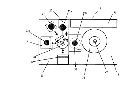
Referring to Figure l, there is shown the overall arrangement of a wafer
sorter/prober
11 including a loader portion 13 and a prober portion 15. The loader portion
13 includes
a "pre-probe", gross defect - inspection unit 17 and a "post-probe", single
chip -
inspection unit 19. The inspection units I 7 and 19 can be allowed to operate
within the
automatic prober because they require no more manual intervention than the
typical
automatic prober. The inspection process is carried out entirely within the
idle time of the
wafers and actually increases the throughput and yield of the electrical test
operation by
eliminating waste and maximizing the potential "good" chips.
The loader portion 13 has a robotic wafer handler 21 which serves to transport
a wafer
23a from one of two storage cassettes 25 or 27 frst to the pre-probe
inspection unit 17
-6-
SUBSTITUTE SHEET (RULE 26)
CA 02259659 1999-O1-06
WO 98/01745 PCT/US97/11862
and later to the prober portion 15. Still later, the handler 21 serves to move
the wafer
from the prober portion 15 to the post-probe inspection unit 19.
The prober portion 15 includes the usual probe card 29 held securely by a
probe card
ring 31. In addition, it includes a prober stage 33 and an alignment unit 35
which perform
the usual functions of properly aligning the wafer 23b and positioning it for
electrical
testing by placing each bonding pad of the wafer into contact with the probe
needles on
the probe card 29.
The pre-probe, gross defect inspection unit 17 performs the pre-alignment,
identification, mapping and gross defect inspection of each wafer. Each task
yields
improvements to the conventional wafer sorting or probing operations.
With pre-alignment, the wafer can be aligned to the chip pattern flat in
addition to the
orientation flat, thereby avoiding rejects and speeding up wafer alignment in
the prober.
(The flat is not always very accurately parallel to chip pattern)
The wafer identification location can be accessed directly from the scanned
image.
No separate OCR or BCR readers are required. The inspection software makes the
image
acquisition and identification from the virtual wafer image while or after the
wafer is
moved on to other operations.
A unique wafer map is generated from each wafer, which precisely identifies
chip
centers with actual wafer outline. A potential good chip is judged from
completeness of
actual pattern image and the coordinate reference based on actual re-
recognizable edge
images.
The pre-probe unit utilizes a rigorous image based coordinate system. Images
show
standard chips where sub-images are given arbitrary numerical values (e.g. I,
2, 4, 6 and
16) to identify the completeness of the chip. If a sub-image is missing or
flawed, the
chip's "score" is reduced by that value. The image illustrates the values of
some edge
chips. Clearly, the reference system provides unique identification even after
the wafer
is diced apart.
_7_
SUBSTITUTE SHEET (RULE 26)
CA 02259659 1999-O1-06
WO 98/01745 PCT/US97/11862
Gross defect damages such as multi-chip scratches, large foreign materials and
metalization errors are located through search procedures simulating the
visual inspection
by an operator looking for such defects. Random defects are noted in the wafer
map for
potential test exclusion if it cannot be positively identified as a pattern
defect. Repeatable
S damages can be correlated and flagged to QC (quality control).
Figures 2A and 2B show one embodiment of the pre-probe, gross defect,
inspection
element 17 of Figure 1. The wafer 23b is held with vacuum by a handler arm 41,
which
has the ability to move the wafer under the scanner rail 37 at a constant
speed and at the
correct vertical (Z) displacement for reading the image data. The arm clears
the vacuum
chuck 39 by a comfortable margin.
Referring specifically to Figures 2A and 2B, the pre-probe inspection unit 17
includes
a scanner array 37 and a vacuum chuck 39 which can be commanded to rotate a
precise
number of degrees. The robotic wafer handling arm 41 provides horizontal Y-
motion of
the wafer, as shown by the arrow 43, as well as the required vertical Z-
displacement, as
shown by the arrow 45. The robotic wafer handling arm 41 which holds the wafer
23b by
vacuum moves the wafer to the pre-probe station 17, then, at constant speed,
moves the
wafer past the scanner array while the scanner records the reflected wafer
image in
memory.
As an alternative, the scanner rail 37 can make the motion which may in some
installations be more practical, considering available space and existing
elements in the
prober.
Referring to Figure 3, there is shown an example of an image from the pre-
probe
scanner 17 prior to any orientation correction. The resulting scan is first
used to calculate
the position of the flat and the wafer center as well as the relative
positions of the wafer
and chuck centers. In this case the image data is not used with full
resolution and a pixel
thresh-hold is used rather than the foil details of the gray scale value. The
image control
software calculates the angle of the flat and rotates the image data to a
normalized
position, then the precise chip locations are determined. In the prober, the
wafer must be
delivered at a certain orientation to match the needles to the pads. Hence,
the system
_g_
SUBSTITUTE SHEET (RULE 26)
CA 02259659 1999-O1-06
WO 98/01745 PCT/US97/11862
controller receives the angular and center corrections needed to operate the
chuck 39 and
handler arm 4 I so that wafer 23b can be delivered to the prober stage 33
centered and be
properly oriented to the probe card 29. This operation is not necessary if the
wafer is
returned to one of the storage cassettes 25 or 27 rather than being
immediatelyelectrically
tested.
A separate microprocessor controls the pre-probe inspection station 17
interfacing
with the handler2l, scanner37, vacuum chuck 39 and a dedicated image-
processingunit.
The control system executes only one scanning operation, storing the data
sequentially
in a two dimensional array so that the array addressing relates uniquely to
the handler arm
I 0 position in one dimension and the individual pixel data points in the scan
line in the other.
To this effect, the hardware is so arranged that the center pixel of the
scanning array 37
is stored at the half point in the allocated memory block (array) as
illustrated in Figure
3. The center of the vacuum chuck 39 lies on the scanner array pixel-line.
The image analysis is to determine the position of the orientation flat 47 and
the
center of the wafer 49. This is accomplished by examining each scan line of
data from
the first reflection found at starting line position 51 to the last line at
position ~53.
Between scan lines S i and 53 the image reveals two flats, a minor one 55 and
the major
orientation flat 47. From line 51 to the flat 55 the half point calculation
gives a constant
value for the X-center line of the wafer each half changing in value according
to the
symmetry of a circle. Beginning at the flat 55, the right half changes faster
than a circle
and, from the beginning of flat 47, the left half deviates from the circle.
From this data the
larger flat 47 is recognized as the desired orientation flat and the end point
coordinates
yield the exact flat angle. Likewise, the symmetry of data locations converts
into the
wafer center position 49 by having determined the X-center line 57 and the Y-
center line
59 of the wafer 23.
It should be pointed out that for the wafer shown in Figure 3 the black,
largely
non-reflective stripe inside the flat 47 is easily detected as a wafer ID
field and thus line
61 is determined as the "pattern flat" which is more desirable and more
accurate. This is
an additional benefit from scanning a wafer instead of the customary detection
of edge.
-9-
SUBSTITUTE SHEET (RULE 26)
CA 02259659 1999-O1-06
WO 98/01745 PCT/US97/11862
Having found the data location representing the wafer image center 49 and the
flat
angle, the image is rotated around the center 49 until the virtual wafer has
an image shown
in Figure 4. This makes the chip search sometimes easier. When the real wafer
must be
reoriented, as is the case for the prober application, the image control must
supply two
angles and one Y-motion offset. Since the wafer can only be moved along the Y-
axis it
is first necessary to rotate the wafer clockwise (the shorter angle to the Y-
axis in this
example) around the chuck center 63 until line 65 passing through the chuck
center 63
and the wafer center 49, coincides with the X-center tine 67 of the chuck 39.
This is
executed by lowering the wafer vertically transferring the vacuum hold from
the handler
arm to the chuck. The chuck is then controlled to rotate the exact clockwise
degrees
around its center 63 formed by the Y-axis 67 and the X-axis 69 of the chuck
39. Next,
the handler arm 41 again picks up the wafer and displaces it along the Y-axis
67 until the
wafer center 49 coincides with the chuck center 63. Finally, the handler arm
41 transfers
the wafer to the chuck 39 which can be controlled to rotate the orientation
flat 47 or the
pattern flat 61 to its final position prescribed by the probing operation. To
arrive at the
position in Figure 4 this amounts to counterclockwise rotation of 180°
plus the angle
between the line 71 passing through wafer center 49 and perpendicular to the
pattern flat
61 and the line 65.
As seen in Figure 4, the image data from the rotated virtual wafer in memory
provides
sufficient information to determine the exact chip positions, wafer LD. and
gross defects.
Simultaneously with the operation of the pre-probe inspection unit 17, the
post-probe
inspection unit 19 will proceed independently to inspect a wafer. Key to the
embodiment
in Figure 1 is the asynchronous operation of electrical testing by the prober
section 15 and
the inspections in the loader portion 13. The prober is the pacing operation
and the
priorities of the handler are to unload and load wafers, maximizing the wafer
throughput.
The second wafer storage cassette 27 provides the means for continuous
operation
between lots.
After the wafer has been electrically tested it is directly delivered to the
post-probe
inspection station 19 (Figure 1 ). The wafer is there held by vacuum while the
robotic
wafer handler 21 delivers the next wafer to the probing operation and pre-
orients and
- 10-
SUBSTITUTE SHEET (RULE 26)
CA 02259659 1999-O1-06
WO 98/01745 PCT/US97/11862
inspects the following wafer in the pre-probe inspect station 17. The
essential post-probe
inspection station configuration is outlined in Figure S.
One embodiment of the post-probe inspection station is shown in Figure 5. As
detailed, the wafer handler 72 is ready to deliver a wafer 23 to the large
vacuum chuck 73.
The wafer may be pre-aligned by virtue of just having been electrically tested
or be
randomly oriented. The wafer handler 72 transfers the wafer 23 to the vacuum
chuck 73
and a dedicated control system proceeds with the post-probe defect inspection.
It should
be noted that even though the vacuum chuck 73 is somewhat larger in diameter
than the
wafer for stability purposes when supporting finer focus requirements for high
magnification, the outer rim is black and does not reflect; hence, scanning
the wafer gives
an image of the wafer as shown in Figure 6.
The inspection sequence begins by making a complete scan like the gross defect
inspection station. As in the pre-probe station, the memory addressing relates
uniquely
to X - Y positioning mechanisms, but in this case, the scanner rail 75 moves
in the Y-
direction 77 while the chuck is stationary. The X-dimension is given directly
by the pixel
elements in the scanner array. The virtual wafer image shown in Figure 6 is
correlated
with the test map resulting from the probing identifying the X-Y center
coordinates of the
chips to be inspected. From this information a table is generated which is
sequentially
used to position the CCD camera 79 so that its center coincides with the
center pixel of
the chip. The rail motion as shown by the arrow 77 is recalculated to include
the fixed
camera offset SO and the angular position of the physical wafer. During a one-
time setup
procedure the camera optics, which includes a zoom lens, is adjusted to
capture one chip
and the offset is adjusted aligning the camera picture center with the chip
center. The
accuracy requirement is determined by uniquely capturing the image of one
targeted chip
and seeing ail of the chip. It is to be understood that micro motion can also
be installed
in the camera. Figure 7A shows the camera 79 being positioned by the scanner
rail 75
over the wafer 23. Referring to Figure 7B, a detail of the current image 95 as
seen by the
camera shows a questionable probe mark 97.
The single chip inspection station is completely self sufficient and can
generate its
own wafer map or correlate the wafer with a previously generated wafer map.
Thus, a
-11-
SUBSTITUTE SHEET (RULE 26)
CA 02259659 1999-O1-06
WO 98/01745 PCT/US97/11862
previously inked wafer can be processed directly, inspecting both ink dots
from the
scanner image representing failed chips, and chip details from good chips
using the
camera image.
Another embodiment of the post-probe or single chip inspection system is
detailed
in Figure 8A. In this case, the camera 79 is fixed in the probing center by a
special insert
ring 99 and the wafer 23 is positioned by the prober stage. Here, the prober
control takes
full responsibility for positioning a particular chip under the camera to
produce a chip
image as shown in Figure 8B. The inspection process takes place on the virtual
chip in
memory. Thus, the indexing time from chip to chip is utilized for inspection
making this
a very efficient operation
The post-probe embodiment can be adapted to printed circuit board (PCB)
inspection
by substitutinga suitable handling and holding device for rectangular PCB's or
films. The
coarse inspection performed on the image data scanned into memory with direct
positional relationship extract suspicious defect candidates. These are often
resolvable at
the scanner resolution level into harmless or damaging defects. In ambiguous
cases the
camera is moved in automatically to obtain the necessary detail s for a
decision.
The post-probe inspection is usually planned as inspecting every wafer but at
least
initially only a limited number of chips. If the initially tested chips fail
it may be desirable
to conduct a 100% inspection. Only electrically good chips are inspected,
thus, the main
criteria is to locate defects which may cause failure during assembly or, more
seriously,
failure after the chip package is installed in the field.
The rules are set according to manual observation and judgments based on
experience. The result from the gross defect inspection can also logically
influence the
sample selection for detailed inspection. Figure 7B shows a critically
positioned probe
mark 97, which may have damaged the "glassification".The main performance
advantage
of the single die inspection is the clear and unambiguous classification in
automatic mode
using the MAMMEX criteria.
-12-
SUBSTITUTE SHEET (RULE 26)
CA 02259659 1999-O1-06
WO 98/01745 PCT/US97/11862
In the post-probe inspection station the wafer 23 is largely stationary after
it is placed
on the chuck 73 apart from minor corrective chuck motions to reach optimum
focus
during image scan-in. The scanner rail 75 on the other hand can move
horizontally in the
Y-direction 77 and the attached CCD camera 79 can be positioned in the X-
direction 81.
S In terms of positional accuracy it must only be sufficient to locate any
unique chip from
the wafer map. The combined effect is the ability to scan in an image of the
whole wafer
and position the camera over any one uniquely identified chip. The single chip
inspection
station can equally well process previously inked wafers, using the wafer
image as a direct
map for picking "good" and "bad" chips for the inspection process.
After post-probe inspection the wafer can be optionally inked or have the map
updated, then replaced in its original wafer storage cassette.
Other embodiments of the invention include running the loader inspection unit
13 as
a separate, free-standing optical inspection system. The handler 21 will in
this case only
move wafers between the inspection units and storage. Such a system can be
made to
1 S qualify for class 1 clean room operation. It is also possible to mount the
post-probe
inspection unit 19 in place of the probe card ring assembly 29, 31. In this
case the prober
becomes a dedicated optical inspection station which can alternate its
operation with
regular probing.
As shown in Figure 4 the image data reveals, when displayed, sufficient
details to
read the wafer ID 83, chip coordinate references 1 O 1, 103 and 1 O5, special
chips 107 and
109, process defects 89 and 91. While all information including chip size can
be found
by global search, the process is simplified by introducing standard data
available from
each wafer type. Normally this includes: Wafer sizes, chip size, flat
orientation, wafer ID
location and type. To simplify the inspection process it is also common to
include the
image of a typical standard chip 93. This sort of "training" is typically
performed only
once when the first wafer of this type appears. The data is then stored as
part of the
retrievable "set-up data" identified by the wafer type name.
Using a standard chip, such as the chip 93 shown in Figure 4, as a model, the
wafer
image in memory is analyzed identifying each chip and classifying them.
Depending on
-13-
SUBSTITUTE SHEET (RULE 26)
CA 02259659 1999-O1-06
WO 98/01745 PCT/US97/11862
an established criteria a coordinate reference chip 101 is established and the
adjacent
chips recorded. In Figure 4, chip 103 is marginal and 105 is partial. In this
example, the
chips are given a binary number based on the completeness of the image. The
exact chip
image is then stored in a separate memory location for future reference.
All special chips like 107 and 109 are recorded with image and pattern defects
like
89 and 91 noted as defects as well as defining the chip as testable and not
testable. Each
defect is analyzed and reduced to a numerical value by a criteria based on
human
inspection methods. The resulting coordinate chip log, duly identified by the
wafer ID 83
is the most efficient wafer map based on actual images. It maximizes the
testable chips
that are potentially good and minimizes total testing time. Since the wafer
map created
is based on actual images it is usable even after the chips are diced apart,
thus, applicable
to pick-and-place assembly operations.
The analysis technique is similar when the single chip image is reviewed. Each
defect
is extracted from the regular pattern and subjected to numerical analysis
which is based
1 S on industry specification (customer modifiable) and skilled human
inspection
methodology. The MAMMEX procedures are adopted to give the desired extraction
and
classification reliability.
- 14-
SUBSTITUTE SHEET (RULE 26)