Note: Descriptions are shown in the official language in which they were submitted.
CA 02263719 2002-08-23
72049-221
- 1 -
HIGH RESOLUTION REAL TIME RASTER IMAGE
PROCESSING SYSTEM AND METHOD
CROSS REFERENCE TO RELATED PATENT
This application is related to commonly owned
United States Patent No. 5,796,411.
FIELD OF THE INVENTION
This invention relates to high speed, high
resolution intelligent electronic imaging, and more
particularly to high speed electronic plateless printing.
More particularly, the present invention relates to Raster
Image Processors ("RIPs") for rapidly generating images.
Still more particularly, the present invention relates to
scaled down, reduced cost high speed dedicated Raster Image
Processor Systems for real time generation of high
resolution images including various different types of image
objects.
BACKGROUND AND BRIEF SUMMARY OF THE INVENTION
Modern high speed electronic "plateless" printing
engines have capabilities not even dreamed of only a few
years ago. For example, the current line of MIDAX~ printing
engines available from Moore Business Forms, Inc. of Lake
Forest, Illinois can print high resolution images on a
continuous "web" of paper moving at a speed on the order of
500 feet per minute. High speed, high resolution color
printing engines are also now available that can print very
high resolution (e. g., 600 dpi) color images on continuous
or sheet-fed paper moving at speeds of on the order of 300
feet per minute or more.
CA 02263719 1999-02-18
WO 98/11503 PCTlUS97/15350
-2-
To provide maximum image flexibility, high performance "intelligent"
electronic printing engines generally take as an input, data defining a
digital
value for each printable location on the printed page. Such locations are
commonly referred to as "pixels" (short for "picture elements"). Although
pixel-based intelligent electronic printing engines can print virtually any
arbitrary image (within the resolution, color and other limitations of the
print
engine), they require a massive amount of input data for high resolution
printing. For example, to print an 8-1/2 inch by 11-inch page at a 600 dots-
per-inch resolution requires 5100 x 6600 = 33.66 million individual pixel
values. High speed printers can print on the order of 300 to 500 pages per
minute (i.e., on the order of 8 pages or more per second) -- and therefore
require in the excess of 300 million pixels (120,000 characters) per second.
The digital value associated with each pixel may nominally be only one
digital "bit" {if the "bit" is "on" the printer should place ink at the
corresponding location; if the "hit" is "off' the printer should not place ink
at
that location). However, modern electronic printing engines provide multiple
(e.g., 4) bits for each pixel to encode gray scale level or one of several
different colors. This requires a data delivery system that can provide on the
order of 1.2 billion digital bits per second.
General purpose digital computers of reasonable cost and complexity
are not capable of supplying print stream data at these incredible rates. The
alternative to real time processing-generating print images "off line" and
storing them for later retrieval by the printer-is not feasible at least
because
the amount of data involved in an average print run is too massive to be
economically stored and rapidly accessed using conventional mass storage
techniques.
SUBSTTTLlTE SHEET (RULE 26)
CA 02263719 1999-02-18
WO 98111503 PCT/L1S97/15350
-3-
To meet the data rate demands of prior generations of intelligent
electronic printing engines, dedicated systems commonly known as Raster
Image Processors ("RIPs") were developed to generate image data based on a
compact input representation such as a PostScript file or other variable data
stream. Some such prior RIP designs could not generate image data in real
time. Thus, these prior RIPs suffered from the drawback that the data coming
in from the input device had to be completely converted before any output
data could be supplied to the output printing device and the print job could
begin to run. This inability to rasterize in real time required each print job
to
be handled in two phases: an off line conversion process, and a later on-line
printing process. This caused delays, and was a severe problem with "just in
time" requirements for delivery of completed print jobs to customers.
Some prior art RIP systems were, however, capable of generating
image data "on the fly" while the print job was running. One example of a
I 5 prior art raster image processor capable of generating image data in real
time
synchronism with printing operations is the."Hybrid RIP" ("H-RIP")
manufactured by Moore Business Forms, Inc. and described in Technical
Reference Manual entitled "H-RIP Technical Manual" (Moore Business
Forms, Inc. 1994). The H-RIP system used dedicated hardware circuitry
controlled by a microprocessor-based master controller to generate rasterized
print image data in real time. Briefly, the prior art H-RIP system accepted,
as
an input, a standardized file format stored on a mass storage device such as
magnetic tape. In this prior design, an intermediate "XI. Data System" read
the input file from the tape and supplied it to the H-RIP for processing. The
H-RIP included an XL, Interface that received and buffered the data from the
XL data system and supplied the data to a microprocessor-based master
controller. The master controller interpreted the input data and created a
SUBSTITUTE SHEET (RULE Z6)
CA 02263719 1999-02-18
WO 98!11503 PCT/US97/15350
-4-
display list specifying the objects to be rendered on the next printed page.
The master controller wrote bit map images of the fonts required to image the
display list representation into a Font Image Memory ("FIM") to make these
objects available for rendering. The master controller then controlled the
S FIM to write the bit map images into a Binary Image Generator ("BIG")
including a pair of full-page bit map memories-thereby "rendering" a
memory image of the entire page to be printed. While one page of image was
being created in one of the full-page bit map memories, dedicated print
engine control and interface circuitry could access an already complete
memory image in the other memory and provide its pixel values to the
printing engine in real time synchronism with paper "web" movement.
Typically, the printer engine could not accept a full page at a time, but
rather
required the data to be presented to it in smaller "chunks" (e.g., in blocks
comprising one or several lines of the image). The H-RIP supplied these
1 S "chunks" to the printer engine in synchronism with the engine's need for
the
data.
Moore's prior art H-RIP system was successful in its own right.
However, further improvements were possible. For example, this prior art H
RIP system does not have sufficient speed and bandwidth to keep up with
advanced high-speed high-resolution print engines now available.
Additionally, the prior art H-RIP was limited to monochrome printing and
had no color capabilities. Furthermore, this prior art H-RIP was limited to
only a single input format, and could not handle graphical images efficiently.
In addition, the prior art H-RIP could work with only a single type of print
engine (a Moore Business Forms MIDAX~ intelligent printer) and was
SUBSTITUTE SHEET (RULE 2fi)
CA 02263719 1999-02-18
WO 98!11503 PCTJUS97/15350
-5-
incompatible with other print engine types. As discussed below, these
shortcomings present severe disadvantages in some applications.
One disadvantage of the prior fI-RIP design relates to its ability to
work with only a single type of printer. The H-RIP was custom-designed to
supply data to a Moore MIDAX~' 300 intelligent printer, and was incapable of
working with any other (non-compatible) printer. However, purchasers
typically have a choice of several different models of intelligent printing
engines, and larger printing facilities may have several different types of
printers for use with different types of print runs. For example, one printer
may be used for production of long print runs, another printer may be used
for production of short runs which require high quality graphics and color,
and a still further printer might be optimal for printing text with simplified
graphics such as lines, boxes and angles. In the past, the print shop had to
purchase a different RIP system for each different printer device since each
RIP was specifically customized for a corresponding particular printer.
The requirement for several different types of RIPs (each of which
may cost several tens of thousands of dollars. assuming they are even
commercially available) led to great expense and confusion. For example,
different RIP systems typically would have completely different cabling,
installation, maintenance and other requirements. Technicians and operators
had to be trained to service each of several dissimilar RIP systems. Spare
parts for many different RIP systems had to be stocked. Software and input
data incompatibilities between the different RIP systems required extensive
logistical coordination to ensure that print jobs were prepared for the right
combination of RIP and uniquely-associated print engine. These problems
SUBSTITUTE SHEET (RULE Z6)
CA 02263719 1999-02-18
WO 98/11503 PCT/US97/15350
may have effectively limited the number of different types of printing
devices a given printing facility could afford to have-thus decreasing the
types of printing services that could be offered to customers.
Prior art RIPs such as the H-RIP also suffered from the disadvantage
that it could only accept input data in a single standardized format. To use
input data in a different format, a print operator would have to convert the
data to the standard format (or use a different RIP designed to accept that
different input format). Each time the printer operator wanted to use a
different input format, he or she would have to convert the data to a format
usable by the RIP associated with the printing device scheduled to print the
job. The printer operator might have to custom tailor or purchase a RIP or
other appropriate conversion system if no existing system would handle the
new, non-standard format. Conversions off line were tedious, sometimes
unreliable, and added substantially to the overall processing time and man
hours required to complete a particular print job. For example, to process a
single print order comprising multiple parts representing different input
formats, the print operator might have to run the first part of the job, and
then
reset the system with a different RIP (which must be done off line) to
interpret a different input format. He or she would then run the next part of
the print set, and possibly thereafter reset and reconfigure the system again
to
run a further part of the job using a still different input format. The
operator
would have to continue in this fashion until the entire multi-part print job
was
completed -- a rather lengthy, cumbersome and inefficient process which was
quite time consuming.
SUBSTITUTE SHEET (RUL>= 26)
CA 02263719 1999-02-18
WO 98/11503 PCT/US97/15350
_ '7 _
Moreover, prior RIP designs such as the H-RIP were not capable of
providing in excess of 300-million pixels per second required to drive high
speed, high resolution monochrome and color electronic print engines. Prior
RIP systems capable of generating color graphic images were limited to
conversion speeds of about 100 million pixels per second-whereas the most
current high resolution color printing engines can require data at rates in
excess of three times that. Throughput and bandwidth problems are
exacerbated by the ever increasing use of complex graphics in the intelligent
imaging process. Processing operations related to graphics and adjusting
portions of the page to accommodate the graphics can be very time-
consuming operations, and full-color high resolution graphics take up a great
deal of storage space. The manipulation of graphic images may also require
the input data to be "screened". to provide appropriate color grades-adding
even more processing time.
Thus, there has been a long felt need for a raster image processor that
can receive inputs in various different formats (e.g., fonts, full color
graphics,
line art, patterns, etc.) from a variety of different input devices and is
capable
of generating outputs in different formats usable by different types of
printing
(or other) output devices. In addition, there is a need to provide a raster
image processor having very high throughput that is also capable of screening
and processing color data. There is also a need to provide a raster image
processor that is modular and expandable to meet varying needs and
requirements. Furthermore, it would be desirable to provide a raster image
processor that can generate high resolution graphics data "on the fly" to
supply in real time to a high speed print engine.
SUBSTITUTE SHEET (RULE 26)
i i
CA 02263719 2002-08-23
72049-221
_ g _
The invention of U.S. Patent No. 5,796,411
provides a raster image processor that can meet these
objectives. It provides a raster image processing system
and method that can keep up with the fastest high resolution
printers now available. It can process images "on the fly"
- that is, generate images from compact input representation
so rapidly that printing can occur substantially in the same
real time as the RIP processor processes the input data.
This has substantial benefit to customers because it allows
print orders to be turned around very rapidly, thereby
satisfying the requirements of "just in time" delivery -
which was not possible using some prior RIP based systems.
In the system of U.S. Patent No. 5,796,411, the
ability to form print images in real time is further
enhanced by the use of a high speed data cache and
associated array disk drive to provide high speed throughput
of data into the system. The disk array may, for example,
store a library of high resolution graphics that can be
accessed "on the fly" as needed in response to the input
data stream. In the preferred embodiment, the disk array
provides very high storage capability and throughput (e. g.,
total storage of 32 gb of information that can be accessed
at a rate of over 50 mb per second). This allows the system
to access graphical images while the particular print job is
underway - enabling nearly simultaneous conversion,
retrieval and printing of graphics and images. A data
caching arrangement coupled to the disk array provides a
FIFO (first-in-first-out) caching/buffering arrangement to
maximize throughput and reduce access time.
To further enhance graphics capabilities, the
system of U.S. Patent No. 5,796,411 may also provide a
custom graphics accelerator that can generate, on the fly,
many "primitive" or simple graphics (e. g., angles, lines,
CA 02263719 2002-08-23
72049-221
- 9 -
boxes, etc.) at the same time that the remainder of the
print image is being generated.
A preferred embodiment of U.S. Patent 5,796,411
may, for example, provide a completely modular architecture
including an XL interface module for input data
synchronization and interfacing, a master controller module
for overall control and coordination, a RISC high speed
processor module for data conversion and manipulation, a
Font Image Memory ("FIM") module for storing bit images of
fonts, a Binary Image Generator ("BIG") module for double-
buffered storage of full-page images, and an Engine Control
Module ("ECM") controlling and interfacing with particular
printer or other output devices.
In the processing and printing of documents, a job
block or file is provided which contains a description of
the entire job to be run including a page by page layout of
the job. Once input is received, the RIP collects and
assembles the characters and other image "objects" in a full
page bitmap memory. The information provided with the job
determines the size and positioning of text and graphics.
The system automatically "remembers" where certain
characters are positioned so as not to duplicate or overlay
new characters.
The system of U.S. Patent No. 5,796,411 has been
able to achieve vastly superior speeds to that of prior RIP
based systems, and can operate at speeds upwards of 300 mega
pixels per second. Part of the success of the system and
its ability to operate at such high speeds, is that the
preferred embodiment is also capable of "screening on the
fly". That is, it can automatically screen data relating to
the images so that the various gray scales or color levels
are correct for a contone printing process. A number of
i
i
CA 02263719 2002-08-23
72049-221
- 10 -
other advantageous features provided by the system described
in U.S. Patent No. 5,796,411 are explained in that
specification.
The advantages and features offered by the system
disclosed in U.S. Patent No. 5,796,411 provide a significant
advance over the prior art. However, such systems can be
quite costly and may provide more capabilities than are
needed to run a particular print job. In certain
applications, flexibility and extended capabilities may be
of lower importance than reduced cost. For example, in some
applications only a specific type of print engine will be
utilized. In other applications, the RIP may only need to
operate within a particular pixel range. Accordingly, it
would be desirable to provide a scaled down raster image
processor specifically for use with a particular print
engine, such as an ink jet printer. Such a scaled down
raster image processor requires more than simply eliminating
optional features.
In accordance with one aspect the present
invention, there is provided a scaled down raster image
processor comprising: a first control circuit which receives
a job description file and, in response to said job
description file, prepares displays lists and transfers
fonts for storage in a font image memory; a scaled down
control circuit that operates in accordance with said
display list and said stored fonts to generate pixel data
representing a digital representation of an image; a bit
image memory associated with said scaled down control
circuit, wherein said bit image memory stores the digital
image representation generated by said scaled down control
circuit; and a personality module for a selected print
engine, wherein said personality module requests and reads
raster data from said bit image memory and provides said
CA 02263719 2002-08-23
72049-221
- 11 -
raster data to said selected print engine to operate said
print engine and thereby produce an image.
In accordance with the present invention, a scaled
down RIP can be tailored to accommodate image generation in
a particular range specifically to efficiently run print
bars at a reduced equipment cost. The disclosed embodiment
processes the input stream for a Moore independent cartridge
array (MICA) ink jet printer, and is still capable of
operating at relatively high speeds (e.g., upwards of 300
feet per minute). However, the preferred embodiment
operates within a limited pixel range of, for example, 1024
pixels wide to 2048 pixels wide. Up to sixteen (16) ink-jet
cartridges in an array may be driven with the preferred
embodiment. Of course, the system could be configured for
additional cartridges or for different types of printers.
In accordance with one aspect of the present
invention, a personality module is provided. The
personality module is responsible for requesting and reading
raster data to build up the staging RAM. The preferred
embodiment utilizes a pair of EEPROMs to control each bar
read according to the position and distance from the other.
Pixel data is then sent to the service station along with
the print bar address. The personality module preferably
outputs the sequence of pixel data to the service station
for imaging, and interfaces the display and keyboard
information and transfers the various offsets to a control
ASIC for rehandling the pixel data at the staging RAM.
In accordance with another aspect of the present
invention, there is provided a method of providing print
information to print engine that prints on a moving web and
has a plurality of printer mechanisms for printing a
plurality of adjacent print bars, wherein at least two of
i
CA 02263719 2002-08-23
72049-221
- 11a -
said printer mechanisms are displaced relative to one
another in the direction of web movement, comprising the
steps of: forming a display list specifying an image;
storing font information in a font image memory; generating
a digital representation of an image based on said display
list and said stored font data, and storing said digital
image representation in a bit image memory; reading raster
data from said bit image memory and directing pixel data to
a staging memory, data for each print bar having the same
base address; for each print bar, adding an offset value to
said base address for said print bar data; and providing
offset print bar data to said print engine in synchronism
with web movement.
BRIEF DESCRIPTION OF THE DRAWINGS
These and other features and advantages provided
by the present invention will be better and more completely
understood by referring to the following detailed
description of presently preferred examples of embodiments
of the invention in conjunction with the drawings, of which:
FIGURE 1 is an example of an overall intelligent
imaging system;
FIGURE 2 shows overall example operations
performed by the raster image processor shown in FIGURE 1;
FIGURE 3 shows an example architecture of the
FIGURE 1 raster image processor in accordance with U.S.
Patent No. 5,796,411;
CA 02263719 1999-02-18
WO 98111503 PCT/US97/15350
-I2-
FIGURE 3a shows the FIGURE 3 raster image processor expanded to
include screening, graphics and data cache capabilities;
FIGURE 4 is a flowchart of example overall control operations
performed by the RISC controller module to control data processing by the
raster image processor;
FIGURE 5 shows an example architecture for the XL interface
module;
FIGURE 6 shows an example architecture for the XL interface
registration controller;
FIGURE 7 shows an example of an overall intelligent imaging system
in accordance with the present invention;
FIGURES 8A and 8B show an arrangement of MICA ink jet cartridges
which may be used in connection with the present invention;
FIGURE 9 shows an example general architecture for a scaled-down
raster image processor in accordance with a preferred embodiment of the
present invention;
FIGURE 10 shows an example of a GPI interface section of a scaled
down controller portion of a raster image processor which may be used in
accordance with a preferred embodiment of the present invention;
SUBSTITUTE SHEET (RULE ~fi)
CA 02263719 1999-02-18
WO 98/11503 PCT/US97/15350
-13-
FIGURE 11 shows an example of a VME interface and font image
memory (FiM) section of a scaled down controller which may be used in
accordance with a preferred embodiment of the present invention;
FIGURE 12 shows an example substructure architecture of a
FIMVME ASIC which may be used in connection with the preferred
embodiment of the present invention;
FIGURE 13 schematically illustrates address decoding which may be
implemented by a FIMVME ASIC in accordance with the preferred
embodiment of the present invention;
FIGURE 14 schematically illustrates a registration operation which
may be implemented by a FIMVME ASIC in accordance with the preferred
I 5 embodiment of the present invention;
FIGURE 15 is an example timing diagram illustrating a write cycle for
storing information in FIM in accordance with a preferred embodiment of the
present invention;
FIGURE 16 schematically illustrates a FIM checksum operation which
may be implemented by a FIMVME ASIC in accordance with the preferred
embodiment of the present invention;
FIGURE 17 illustrates an example substructure architecture of a main
controller in accordance with the preferred embodiment;
SUBSTITUTE SHEET (RULE 26)
CA 02263719 1999-02-18
WO 98/11503 PCTlUS97/15350
- 14-
FIGURE 18 illustrates an example display list information provided in
a set of thirty-two bit longwords;
FIGURE 19 is an example useful in illustrating a preferred manner in
which a character from font image memory (FIM) is placed in bit image
memory (BIM);
FIGURE 20 is an example circuit useful in illustrating operation of a
main controller in accordance with the present invention;
FIGURE 21 shows an example substructure architecture of the
personality module ASIC; and
FIGURE 22 illustrates a technique for compensating for relative
1 S displacements of print cartridges in the direction of web movement.
SUBSTITUTE SHEET (RULE 26)
f
CA 02263719 2002-08-23
72049-221
- 15 -
DETAILED DESCRIPTION OF THE DRAWINGS
In describing the features, characteristics and
advantages of the present invention, reference will be made
initially to a preferred larger-scale raster image processor
described in connection with U.S. Patent No. 5,796,411.
Against that background, the present invention will be
described with primary reference to FIGURES 7 through 23.
It should be appreciated that the following description is
directed to a preferred implementation, and that various
modifications, adjustments and variations may be made
according to particular needs. The present invention is not
intended to be limited to the described embodiment. For
example, although the present invention is described in
connection with a MICA ink-jet printer, other printers can
be utilized in which case appropriate changes and
substitutions may be made in the described implementation.
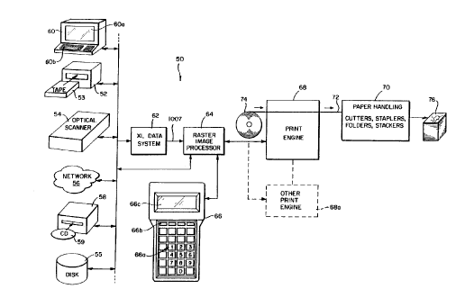
FIGURE 1 shows an intelligent imaging system 50.
System 50 performs the overall task of assembling digital
image "objects" based on input digital data to create a
visible image that can be viewed by a person. In this
particular example, the visible image is printed onto a
medium such as moving a paper "web" 72 to produce finished
printed matter 76 that can be distributed and read or
viewed.
Overall Intelligent Imaging System 50
Intelligent imaging system 50 may include various
input data sources such as a magnetic tape drive 52, an
optical scanner 54, a network 56 and a optical disk drive
system 58. In addition, system 50 includes a "front end"
computer system 60; and XL data system 62; and a raster
image processor 64.
CA 02263719 1999-02-18
WO 98/11503 PCT/US97/15350
- 16-
Components 60, 62 and 64 are electronic devices that create, store,
manipulate and process digital data to produce a digital representation of a
visible image. In this example, system 50 further includes a print engine 68
and a paper handling mechanism 70. The print engine 68 may be a high
resolution, high speed monochrome or color conventional print engine
device, such as, for example, a Moore Business Forms MIDAX~ print
engine, a Scitcx print head, or an Indigo high speed color printer.
The print engine 68 shown in FIGURE 1 prints on a continuous "web"
72 of paper supplied, for example, from a large paper roll 74 at high speeds
of
up to 300 to S00 feet per minute. Print engine 68 includes electronic print
heads that print images on web 72 as the web travels through the print engine
(i.e., "plateless printing"). The printed web 72 is processed by conventional
paper handling mechanisms 70 (e.g., cutters, staplers, gluers, folders,
collators, stackers, etc.) to provide finished printed products 76.
The "raw materials" for the images to be printed by print engine 68
come from data sources 52-58. The system 50 accepts input data in a variety
of forms including for example:
Images
- fonts such as outline font formats (e.g., Adobe type 1,
Post Script, true type and bit stream);
- pre-generated Moore XLF format fonts;
LineArt in compressed or uncompressed format;
ConTone or full color graphics images;
Objects
SUBSTITUTE SHEET {RULE 26)
CA 02263719 1999-02-18
WO 98111503 PCT/US97/15350
- 17-
- dynamic MCCS (Moore Command Code Stream)
formatted data stream
- standard JIB oriented objects;
Screening tables;
Color lookup tables;
Executable software for raster image processor 64 to execute;
Job description file instructions including, for example, input
text.
Various ones of data sources 52, 54, 56 and 58 may supply these
various types of input data as may be convenient. For example, input text to
be printed may be stored on magnetic tape 53 or magnetic disk 55. Optical
scanner 54 may be used to scan in photographs or other images for storage on
disk 55 and later retrieval. Optical drive 58 accepts optical disks 59 that
may
store a variety of information including, for example, line art, fonts,
executables, etc. Network 56 may connect system 50 to other similar systems
50 and/or other computing and/or storage devices located locally or remotely.
"Front end" image handling system 6U enables users to input and
correct full color images as well as line art, fonts and Post Script files.
Front
end 60 may be, for example, a general purpose digital computer such as a
high-capability personal computer including a display 60a and a keyboard
60b. Front end 60 need not be co-located with the rest of system 50, but
could be remote and communicate with XL data system 62 and raster image
processor 64 via magnetic tape 53 and/or network 56, for example. Thus, for
example, in one configuration the front end 60, optical scanner 54, optical
drive 58 and disk 55 might be located remotely to the rest of the system 50,
SUBSTITUTE SHEET (RULE 26)
CA 02263719 1999-02-18
WO 98/11503 PCT/US97/15350
-18-
and produce as its "output" a job description file stored on magnetic tape 53.
Magnetic tape 53 could then be physically carried to a production floor and
inserted into another magnetic tape drive 52 coupled to XL data system 62,
raster image processor 64 and print engine 68.
The "human" job coordinator operates front end 60 to perform a
variety of tasks. For example, the human operator may, using front end 60,
select and collect images from the various data sources such as continuous
tone pictures scanned using optical scanner 54, continuous tone images stored
on a Photo CD optical disk 59 or Post Script files supplied by magnetic tape
53 and/or disk SS (or authored using the front end). The human operator also
uses front end 60 to collect all line art such as graphics and logos, from
either
scannable line art or from Post Script files defining the graphics. The human
operator also uses front end 60 to identify all fonts needed for a particular
1 S printing job, and if necessary, uses front end 60 to convert the font
layout to
an acceptable format. The job coordinator also uses front end 60 to select job
layout and configuration. He or she will select and locate all objects to be
printed on the finished printed products 76. The job coordinator creates,
using front end 60, a "job description file" and supplies it plus all
necessary
fonts to raster image processor 64 via XL Data System 62 (for example, the
job description file may be stored on magnetic tape 53 for later retrieval).
Raster image processor 64 is an electronic device that creates an image
in computer memory based on the job description file provided by front end
60, and sends the digital image to print engine 68 for printing. More
particularly, raster image processor 64 rasterizes variable combinations of
text, graphics and continuous tone images at high speed based on an inputted
SUBST1TL1TE SHEET (RULE 26)
CA 02263719 2002-08-23
72049-221
- 19 -
job description file, and outputs the rasterized image in
digital form to print engine 68 in real time synchronism
with the operations of the print engine. Raster image
processor 64 monitors the travel of web 72 through print
engine 68 and synchronizes its operations with web travel.
Raster image processor 64 also controls print engine 68 to
provide correct print registration of the images the print
engine prints on web 72. Raster image processor 64 thus
coordinates with XL data system 62 to receive portions of
the inputted job description file as they are needed,
creates electronic images (in memory) to be printed on web
72, and supplies those electronic images in digital form at
the rates, resolution and formats required by print engine
68.
The raster image processor 64 may be capable of
driving a number of different print engines or other output
devices including, for example, Moore's MIDAX~ print engine,
Scitex print heads, and other imaging devices. FIGURE 1
indicates this by showing another print engine 68a that may
be coupled to the output of raster image processor 64
instead of print engine 68. In the preferred embodiment of
U.S. Patent No. 5,796,411, no configuration changes to
raster image processor 64 are required if the other print
engine 68a is compatible with print engine 68. However, if
the other print engine 68a is not compatible, then a simple
swap of a single plug-in electronic control module within
raster image processor 64 for another is all that would be
required to allow the raster image processor to work with
the other print engine.
The human operator may control raster image
processor 64 through a hand-held data display terminal 66
that includes a keypad 66a, an array of light-up indicators
(e. g., light emitting diodes) 66b, and an LCD display 66c.
CA 02263719 1999-02-18
WO 98/11503 PCTlUS97/15350
-20-
Terminal keypad 66a includes mode keys that select modules within raster
image processor 64 to be controlled by the terminal. The human operator can
use terminal 66 to read status information and error conditions, control
operating parameters (e.g., feet per minute, offset, registration mode, type
of
registration, etc.), invoke reset and download, and perform a variety of other
control operations.
Raster Image Processor Operations
FIGURE 2 shows the overall operations performed by the larger scale
raster image processor 64. The "front end" 60 supplies a job description file
80 to the raster image processor 64. This job description file 80 typically
contains a compact digital representative description how each of the pages of
the finished printed product 76 will look. That is, for each different page to
be imaged, a job description file will specify all text to appear on the page,
identify the fonts to be used, specify any graphics or line art to be
included,
and also specify (if color imaging is employed) what colors are to be used.
Job description file 80 essentially provides a complete representation in
digital form of the entire print "job"-which may consist of many different
pages of images.
Raster image processor 64 converts the job description file 80 into one
or more "dlSDlaV llStS" ~2_ RaCIPT imaoP nrnrPCenr fd rrnatn~ ~ .a:~.,l~..
t:~t V'7
for the next (and each) page to be imaged. Display list 82 specifies objects
and their corresponding positions on the page as well as color/density
information and other characteristics. For example, display list 82 typically
specifies text information to be imaged, the position of the text on the page,
and the font the text is to be imaged in.
SU8ST1TUTE SHEET (RULE 26)
CA 02263719 1999-02-18
WO 98/11503 PCT/US97/15350
-21 -
Raster image processor 64 interprets the display list 82 as a list of
instructions specifying the next page to be imaged. Raster image processor
64 constructs a digital representation of a complete image in memory in
accordance with the instructions contained within the display list 82. Raster
image processor 64 interprets the display list 82 to identify all "fonts"
(e.g.,
type styles) required to image the next page. The raster image processor then
writes bit map images of the necessary fonts info a "font image memory"
("FIM") 400 so they are available for imaging. Raster image processor 64
also parses the display list 82 to identify all graphics images that need to
be
supplied to image the page. The raster image processor can generate some
simplified types of graphics "on the fly". For example, if a special
component called a "graphics accelerator" module 900 is present, the raster
image processor 64 can generate curved lines, geometrical shapes, ete. "on
the fly" in real time and supply them on an as-needed basis in response to the
instructions within the display list 82.
For color imaging, raster image processor 64 may add color
information to the font information supplied by font image memory 400 (and
also to the graphics generated by graphics accelerator 900) -- all as
instructed
by the display list 82.
The raster image processor 64 can also access pre-stored graphics such
as color images, line art, etc., from a graphics library stored in a "data
cache"
800. The raster image processor 64 may control "data cache" module 800 (if
present) to retrieve and supply the appropriate graphics images as needed and
specified by display list 82.
SU85T1TUTE SHEEN' (RULE Z6)
CA 02263719 1999-02-18
WO 98/11503 PCTlLJS97/15350
-22-
Once the various "objects" to be imaged are ready to be supplied,
raster image processor 64 assembles them together to form a complete digital
representation of the final image. This digital representation is stored in a
"Bit Image Memory" 512. In a preferred embodiment of the larger scale
raster image processor, Bit Image Memory 512 has "double buffers"-i.e., it
has a pair of duplicate memories 512a, 5 I2b each of which can store an entire
image. This allows raster image processor 64 to output a completed image to
the output device at the same time that it is creating the next image in the
bit
image memory S 12 in real time.
In this example, each of Bit Image Memories 512a, 512b comprises a
full page "bitmap" having discrete storage locations positionally
corresponding to each position on the page that can be filled in with a dot.
This bit mapped memory image may comprise four "bit planes" to provide a
total of sixteen (24) color or monochrome density values. The graphics and
line art provided by data cache 800 may supply the appropriate color
information directly to Bit Image Memory S 12.
When raster image processor 64 has finished storing a completed page
image into one of Bit Image Memories 512a, 512b, it ceases accessing that bit
image memory and begins working on a new image in the other Bit Image
Memory. Output circuitry then accesses the completed image and output the
data in a sequence and at a rate required by the print engine 68 being used.
Thus, for example, raster image processor 64 may supply the completed bit
mapped image one line at a time or multiple lines at a time as required by the
print engine 68, and does so at timing synchronized with the movement of
web 72 through print engine 68. While one part of the raster image processor
SUBSTITUTE SHEET (RULE 2fi)
CA 02263719 1999-02-18
WO 98/11503 PCTIUS97/15350
- 23 -
64 is accessing the completed memory image in Bit Image Memory S 12a,
another part of it may at the same time be building the next page image in its
duplicate binary image memory 512b -- and still another part of the raster
image processor may be converting another portion of job description file 80
into a new display list 62 for the second-to-next succeeding page.
Architecture of arger Scale Raster Image pr0,_ cep
FIGURE 3 shows an example modular architecture for larger scale
raster image processor 64. Raster image processor 64 may be fully modular,
and constructed based on a generalized bus architecture and associated back
plane that allows the different modules (preferably each of which comprises a
single printed circuit board) to be replaceably plugged in and out. This
modular architecture provides easy expandability to add additional
capabilities (compare FIGURES 3 and 3A), and also allows some modules to
be swapped out for other modules to adapt to different requirements (e.g.,
different output devices such as different print engines).
In the example shown in FIGURE 3, raster image processor 64
includes an XL interface module 100, a master controller module 200, a RISC
controller 300, a font image memory ("FIM") module 400, a binary image
generator ("BIG") module 500, and an engine control module ("ECM") 600.
A VME bus 1000 provides communication between XL interface module
100, master controller module 200 and RISC controller module 300. An "R-
BUS" 1002 allows communication (image, commands) between RISC
controller module 300, FIM 400, BIG 500 and ECM 600. An F-BUS 1004
allows transfer of image date (e.g., fonts and logos) between the FIM 400 and
SUBSTITUTE SHEET (RULE Zfi)
CA 02263719 1999-02-18
WO 98/11503 PCTIUS97/15350
-24-
the BIG 500. A P-BUS 1006 transfers final form image data from BIG 500 to
ECM 600.
As shown in FIGURE 3a, R-BUS 1002 also provides communications
to optional enhancement modules such as, for example, a screening module
700, a data cache module 800 and a graphics module 900. F-BUS 1004
allows transfer of image date between the FIM 400 and/or the BIG 500, and
the graphics module 900. In addition, in this expanded configuration, data
cache module 800 may communicate data to screening module 700 over a DC
(data cache) bus 1010, and screen module 700 may communicate data to BIG
700 via a SCR (screen) bus 1012.
Briefly, the XL interface module 100 accepts the job description file
80 from an XL Data System 62 and supplies it for processing to master
controller module 200. Master controller module 200 converts the job
description file 80 into display lists 82, and supplies the display lists to
RISC
controller module 300 for imaging. The RISC controller module 300
coordinates the operations of FIM 400 and the BIG 500 (which contains the
Bit Image Memories 512a, 512b) to generate the digital representation of the
image based on the display list 82 for the next page to be imaged. The ECM
600 breaks the completed digital representation up into suitably sized
"chunks" and provides them to print engine 68 exactly at the time the print
engine needs them to print the next portion of the image.
The (optional) graphics module 900 generates vector graphics "on the
fly" based on instructions from RISC controller module 300, and also is
capable of efficiently de-compressing and~or scaling image files. The
SUBST1TL1T~ SHEET (RUL~ 26)
CA 02263719 1999-02-18
WO 98111503 PCT/LTS97/15350
-25-
(optional) data cache module 800 stores a graphics library and supplies
required prestored graphics information to screen module 700 in real time.
Screen module 700 "screens" contone image files and provides the resulting
pixelized data values to BIG 500.
S
More Detailed Description of Lar er Scale
Raster Image Processor Or~erations
FIGURE 4 is an example of a sequence of control steps performed by
RISC controller module 300 to coordinate the various activities performed by
raster image processor 64. Raster Image processor 64 and its associated
RISC controller 300 begins operations by initializing (block 84). Then, RISC
controller 300 looks for a display list 82 to process {block 86). Once the
RISC controller 300 receives a display list 82, it begins parsing it (e.g.,
from
top to bottom) to determine the type of objects it specifies (block 88). If
the
display list 82 "instruction" specifies a color, then RISC controller 300 sets
the default color to the specified color for use in further rendering of text
and
graphics (block 90). If an "instruction" within display list 82 specifies text
(exit block 91), RISC controller 300 sends a command to the FIM 400 (block
95) specifying the characteristics of the text characters to be imaged. If the
display list 82 "instruction" specifies a graphic (exit block 92), RISC
controller 300 sends a command to the graphic module 900 specifying the
characteristics of the graphic to be generated (block 96). If an instruction
within display list 82 specifies an image (exit block 93), RISC controller 300
sends a command to the Screen module 97 (block 97). This parsing process
continues in an interactive fashion until RISC controller 300 encounters an
"end of page" instruction (block 94) -- at which time it checks hardware
status (block 99) and "returns" to wait for arrival of the next display list
86 to
SUBSTITUTE 5HE~T (RULE 26)
CA 02263719 1999-02-18
WO 98111503 PCT/US97/15350
-26-
process. Meanwhile, each of FIM 400, Graphic module 900 and Screen
Module 700 writes its respective output into the bit image memory 512 within
BIG 500.
More Detailed Discussion of La her Scale
Raster Image Processor Modules
The overall operations and architecture of raster image processor 64
are described above. The following provides additional, more detailed
descriptions of each of the various modules within the larger scale raster
image processor 64.
XL Interface Module i00
FIGURE 5 shows an example of an overall architecture for XL
interface module 100. XL interface module 100 in this example is a
microprocessor-based interface device that:
provides communications between the XL data system
62 via the GPI bus 1007;
~ provides web synchronization and registration control
for the raster image processor 64;
receives data from the XL data system 62 and buffers it
into a FIFO (up to 16 mb); and
drives operator control terminal 66.
SUBSTITUTE SHEET (RULE 26)
CA 02263719 1999-02-18
WO 98/11503 PCT/US97/I5350
-27-
In this example, XL interface module 100 includes a VME bus interface and
data FIFO block 102, a GPI bus interface 104, a serial communications and
operator interface block 106, a registration controller block 108, and a
microprocessor and interrupt control block 110. An internal bus 112 allows
blocks 102-110 to communicate among themselves. In addition, a further
data path 114 between VME interface and data FIFO I02 and GPI interface
104 allows information to be rapidly transferred from the GPI bus 1007 and
the VME bus 1000.
The overall operation of XL interface module 100 is controlled by
microprocessor and interrupt control 110, which may include a Motorola
680180 microprocessor with 64 K-bytes of EPROM, 256 K-bytes of RAM
and a decode and interface PASIC. In this example, microprocessor 110
controls all functions of XI, interface module 100 except for those of data
FIFO 102.
Registration controller 108 synchronizes the imaging operations of
raster image processor 64 with the travel of web 72. Registration controller
accepts web synchronization signals from various encoders and scanners
disposed on print engine 60 to monitor the position and travel of web 72. In
response, registration controller 108 generates print registration control
signals which it provides to ECM 600. ECM 600 uses these print registration
control signals to synchronize itself and print engine 68 with the movement
and position of web 72.
FIGURE 6 shows a more detailed functional diagram of registration
controller 108. The registration controller 108 includes signal conditioning
SUBSTITUTE SHEET (RULE 26)
CA 02263719 1999-02-18
WO 98111503 PCT/US97115350
-28-
devices 116, 118 and 120 to condition the web synchronization signals it
receives. Registration controller 108 also includes registration counters 122,
124, 126 (implemented in this example by one or more PASICs --
programmable application-specific integrated circuits) that keep track of the
position of web 72 relative to the current (and next) page. An array of
multiplexors 128-134 is used to select between the various web
synchronization signals depending on the particular registration mode being
used. The following table shows examples of how top-of form is generated
in each of five different registration modes:
MODE HOW TOP OF-FORM IS GENERATED
Sensemark Optical scanner senses a preprinted mark on
the form
Pinwheel Tractor-driven encoder with resolution of 36
pulses per inch
Tight Web XL Data System's CUE signal
Plain PaperRaster or pitch encoder
Fake Mode Internally generated rasters Test only
Based on this processing, registration controller 108 generates a top-of form
(TOF) control signal that it supplies to microprocessor and interrupt
controller 110. This TOF signal is used as a primary synchronization control
signal to synchronize raster image processor 64 with web 72 movement.
Referring once again to FIGURE 5, GPI bus interface 104 includes
two main functional sections. The first section receives data from GPI bus
1007 and passes it to the on board data FIFO 102 via data path 114.
Microprocessor 110 can also pass data to data FIFO 102, using this channel
during stand-alone operation. A second section of GPI interface 104 is used
SUBSTITUTE SHEET (RULE 26)
CA 02263719 1999-02-18
WO 98/11503 PCT/US97/15350
-29-
to pass message data back-serially-to the XL data system 62. The GPI bus
1007 in the preferred embodiment includes data path 1007a and a message
output path 1007b for these respective purposes.
The serial communications and operator interface block 106 of XL
interface module 100 comprises an 8-channel serial controller chip, serial bus
drivers, and interrupt control circuitry i'or microprocessor i 10. These
channels enable all functional parts of raster image processor 64 to
communicate with XL interface module 100 and display terminal 66.
'fhe VME interface and data FI1~0 block 102 can be, in this example,
configured with 4, 8 or 16 mb of memory. 'this block 102 is used to buffer
data from the XL Data System 62 or other host data system to be accessed by
master controller 200 across the VME bus 1000. The control logic within
VME interface and data FIFO 102 may, for example, comprise a pair of
PASICs. One of these PASICs may control the FIFO input, while the other
may oversee the reading of the FIFO in the VME bus interface and decode.
Interrupt arbitration for the three VME interrupts provided (FIFO empty,
TOF and host reset) are also handled by this block 102 in this example.
In more detail, the FIFO controller section of block 102 may consist of
DRAM and associated DRAM controller that can be configured as a 4, 8 or
16 Mb FIFO. Data from an input latch may be read and put into the main
FIFO, and then moved into a smaller on-board 512-byte FIFO as the smaller
one is emptied through the VME bus controller onto the VME bus i 000. The
DRAM controller in this example produces three main cycles: read, write
and refresh. The controller looks for data to be available in its input latch.
SUBSTiTUTF SHEET (RULE 26)
CA 02263719 1999-02-18
WO 98/11503 PCTIUS97/15350
-30-
When data becomes available, the controller performs a write cycle and
writes the byte into DRAM. When the FIFO is not empty, and the 512-byte
FIFO is not full, then a read cycle is performed to move the byte ii-om the
main DRAM FIFO to the 512-byte output FIFO. The DRAM controller also
produces a refresh approximately every 15 ms to maintain valid data in the
DRAMS.
The VME bus interface section within block 102 in this example
contains a PASIC and other circuitry which controls the VME bus decoding
and arbitration, as well as the FIFO output data shifting. The FIFO data can
be accessed by either byte, word or long word in this example. Data is read
from the S 12-byte FIFO when not empty, and shifted into an output shifter.
The output shifter is a 4-byte shift register in this example that shifts one
byte
at a time, down to the least significant bit location. As the least
significant bit
location is filled, the next byte is shifted into the next least significant
position until all four bytes are filled. When a byte-wide VME read occurs,
the first byte is shifted into the shifter. Next, the three remaining bytes
and a
new byte from the 512-byte FIFO are shifted simultaneously to fill the shifter
again. This also occurs for word and long word FIFO accesses. Block 102
maintains a status register readable by main controller module 200 over the
VME bus 1000 that indicates FIFO status and data availability. The VME
interface portion of block 102 also includes 2 kB of dual-port RAM in this
example that accessible by both the microprocessor 110 and by master
controller 200 and RISC controller 300 over the VME bus 1000. This shared
RAM is used for control and communication between XI, interface module
and master controller module 200.
SUBST1TLJTE SHEET (RULE 26)
CA 02263719 2002-08-23
72049-221
- 31 -
Master Controller Module 200
Master controller module 200 includes a Motorola
68040 microcontroller in this example with an associated 4
Mb of RAM. Master controller module 200 is the master
controller of raster image processor 64, and provides for
communication between the XL interface module 100 and RISC
controller module 300. The master controller module 200,
which is based on a prior master controller design used in
the prior art Hybrid RIP product, performs various control
and processing operations under software control. For
example, master controller module 200 maintains a Job
Information Block (JIB) that contains information for each
line to be imaged including start information, font,
rotation, placement and line length. Master controller
module 200 also maintains a Font Address Memory that stores
the starting pointers of each character within FIM 400. As
master controller module 200 processes job information
passed to it by XL interface module 100, it passes the
information over VME bus 1000 to a memory within RISC
controller module 300.
Additional details concerning the structure and
operation of RISC Controller 300, Font Image Memory 400,
Binary Image Generator 500, Engine Control Module 600,
Screening Module 700, Data Cache 800, and Graphics Module
900 are provided in commonly owned U.S. Patent No.
5,796,411. These details are not repeated here.
The Scaled Dowa Raster Image Processor
The foregoing high resolution real time raster
image processing system and method provides a significant
advance over the prior art. Nevertheless, not all
situations warrant the speed, power and flexibility provided
by the
CA 02263719 1999-02-18
WO 98/11503 PCTII1S97115350
-32-
raster image processing technique described above. Even eliminating
optional features (compare FIGURES 3 and 3A) leaves a system having
speed, power and flexibility which is often not needed or desirable for a
particular situation. Accordingly, the present invention allows for a scaled
S down, reduced cost, high speed raster image processor system capable of
generating high resolution images in real time.
Referring now to FIGURE 7, an example of an overall intelligent
imaging system in accordance with a preferred embodiment of this invention
is shown. The intelligent imaging system of FIGURE 7 is similar to that of
FIGURE 1, and like features are identified with like reference numerals. In
the system of FIGURE 7, the scaled down raster image processor 2064
including a personality module (discussed below) which tailors the operation
of the raster image processor 2064 for a particular print engine. The
exemplary embodiment disclosed here is described in connection with a
Moore~ Intelligent Cartridge Array (MICATM) ink jet system. Of course,
other print engines may be employed.
A MICA print system is shown schematically in FIGURES 8A and
8B. Figure 8A is a front view illustrating a plurality of individual ink jet
cartridges C 1-C 16 mounted on specially designed brackets 2102a through
2102f. As seen better in FIGURE 8B, each of the brackets 2102a through
2I02b includes a pair of parallel rails. Each bracket 2102a through 2102b
spans across the web 72 in a direction perpendicular to the direction of web
movement. Ink jet cartridges C 1, C7 and C 13 are mounted on bracket 2102f;
ink jet cartridges C2, C8 and C 14 are mounted on bracket 2102e; ink jet
cartridges C3, C9 and C 1 S are mounted on bracket 2102d; ink jet cartridges
SUBSTITUTE SHEET {RULE 26)
CA 02263719 1999-02-18
WO 98/11503 PCT/US97/15350
- 33 -
C4, C 10 and C 16 are mounted on bracket 2102c; in jet cartridges CS and C 11
are mounted on bracket 2102b; and in jet cartridges C6 and C 12 are mounted
on bracket 2102a.
Each of the ink jet cartridges includes a print head arranged adjacent a
roller. In particular, the ink jet cartridges mounted on bracket 2102a (i.e.,
cartridges C6 and C 12) have print heads adjacent roller 2104a; the ink jet
cartridges mounted on bracket 2102b (i.e., cartridges CS and C 11 ) have print
heads adjacent roller 2104b; etcetera. Guide rollers 2106 and 2108 arc
provided to facilitate web travel. FIGURE 8B shows that the centerlines of
the respective print heads pass through the center of the associated roller
2I04a through 2104b.
As can be seen in FIGURE 8A, each of the ink jet cartridges is
arranged slightly adjacent other cartridges to obtain print coverage over a
printing width PW. Thus, as the web 72 moves from paper roll 74 to paper
handling equipment 70, the ink jet cartridges C 1 through C 16 print sixteen
adjacent bars. If a wider printing width PW is desired, additional cartridges
could be provided.
Referring back to FIGURE 7, the scaled down raster image processor
2064 is capable of performing ,fewer operations than is the raster image
processor 64 of FIGURE 1 (see FIGURE 2). For example, the preferred
embodiment of the scaled down raster image processor, as configured for use
with the MICA printing system, does not provide color, grey scale, or pattern
(e.g., cross-hatching) printing, includes no graphics board, no image cache,
and no screening module. Thus, there are substantial cost savings.
SUBSTITUTE SHEET (RULE 26)
CA 02263719 1999-02-18
WO 98/11503 PCT/LTS97/15350
-34-
FIGURE 9 illustrates an example architecture for a scaled down raster
image processor 2064. The preferred embodiment of the scaled down raster
image processor utilizes a portable cabinet having a generalized bus
architecture and associated back plane that allows different modules (e.g.,
S printed circuit boards) to be replaceably plugged in and out. The
architecture
permits flexibility by permitting a particular module to be swapped out for
other modules. I~or example, a module designed for use with the MICA print
system could be replaced by another appropriate module if a different print
engine was employed.
In the example shown in FIGURE 9, the scaled down raster image
processor 2064 includes a master controller module 2110, a scaled down
controller module 2112, and a personality module 2114. The master
controller module 2110 decodes GPI data, rotates font data and transfers data
1 S to FIM. During production it sends command codes, font addresses, X and Y
positions, X and Y sizes, combination logic control signals, line draws, and
form sizes. It also processes errors and the corresponding message blocks,
then sends them back to the GPI.
1'he scaled down controller 2112 stores font data, decodes and carries
out display lists, builds BIM and outputs pixel data to the engine control
module (in this case, the personality module). The scaled down controller
also keeps track of raster pulses and starts the exact print position.
The personality module 2114 receives pixel data and directs the pixel
data to the staging RAM according to bar position and bar offset. As
discussed below, the bar offset compensates for displacement of the ink jet
SUBSTiTUT~ SHEET (RUL~ 2fi)
CA 02263719 1999-02-18
WO 98/11503 PCT/US97I15350
-35-
print cartridges relative to one another in the direction of web movement.
The personality module also outputs the sequence of pixel data to the print
engine service station for imaging, it interfaces display and keyboard
information, and transfers top-of form (TOF) offsets and bar offsets to a
S control ASIC for rehandling pixel data at the staging RAM. The personality
module 2114 may be provided as a daughter board to the scaled down
controller 2112. This allows the personality module to be readily replaced if
desired.
The cabinet preferably provides a number of outside connectors to the
modules. For example, an RS232 connection is provided for interfacing and
data communications with the hand-held controller 66 (FIGURE 7). The
hand held controller is preferably a QTERM-II unit from QSI Corp, Salt Lake
City, Utah. Additionally, a GPI bus 1007 is provided. The GPI bus is
preferably a shielded electrical cable that acts as the pathway for print data
generated by the raster image processor, control signals by the XL Data
System 62, and status messages returned by the print device.
Although the system is described in connection with a hand-held
controller 66, it is also possible to utilize, for example, built in keyboards
and
display screens. The preferred Q-Term hand held unit 66 includes forty
membrane keys, six LEDs, and a four line by twenty character LCD display.
The top row of keys may operate as "MODE" keys which are used to select
the board/function that will be communicated with by the Q-Term controller
66.
SUBSTITUTE SHEET (RULE 26)
CA 02263719 1999-02-18
WO 98/11503 PCTIUS97115350
-36-
When a MODE key is pressed, a corresponding LED will light
continuously to indicate the selected operating mode. For a given mode, a
particular RIP board has control of the display, and pressing any of the "non-
mode" keys will send a key code, corresponding to the key pressed, back to
the selected board. If a different mode key is selected, the board which is
presently controlling the hand-held terminal 66 surrenders control to the new
board.
Examples of the various modes include Registration, RIP and Setup.
The Registration and Setup modes are the primary modes which an operator
controls the MICA print engine.
In the Registration mode, the user can specify to the scaled down RIP
2064 the type of registration to be used for a particular job. For example,
the
operator can specify the direction of web travel, relative to a MICA
registration sensor. The operator can also adjust a top-of form (TOF) offset.
When in the Registration mode, the Q-Term display preferably shows the
version of software that is being used and the current date; the second line
may display the size of the form being printed (e.g., FS = 27.00) and the
current mode of the scaled down RIP 2064 (e.g., NORMAL); the third line
may display the resolution of the current print job, which might range for
example from 72 dpi TO 360 dpi; and the fourth line can display what offset,
if any, is in effect and speed parameters such as maximum available speed
and current speed. In the preferred embodiment, the maximum offset
increment is one inch and the minimum is one pixel. The maximum offset
value is the form size minus on inch.
SUBSTITUT~ SHEET (RULE ~6)
CA 02263719 1999-02-18
WO 98/11503 PCT/US97/15350
-37-
The web travel direction is preferably specif ed through an encoder
phase change menu. The setting is chosen in accordance with the web travel
direction and the position of a web travel encoder to inform the system
whether the encoder will turn clockwise or counterclockwise. A TOF offset
menu allows the operator to adjust the top-of form offset. Both the offset
movement and the total offset may be adjusted.
In entering the Setup mode, the Q-Term display indicates the print
engine speed in feet per minute, and shows the status of error status
indicators. once the Setup mode is entered, the operator may set individual
cartridge parameters. For example, a malfunctioning cartridge could be
disabled, and the coarse and five bar offsets (i.e., the "Y" position of data
on
the form) can be adjusted. An option is preferably provided to return all
offsets to default values.
The master controller 2110 is preferably a commercially available
Motorola MVME I 62 card. A number of bus structures are provided on the
modules to operate with the master controller. For example, the scaled down
controller 2112 includes a VA ( 1-31 ) bus which operates as a VME address
bus. VAO is defined internally by the MVME162 DSO and DS1 (lower and
upper words, respectively). As discussed further below, the VA bus address
is decoded by a FIMVME ASIC 2122 of the scaled down controller before
addressing other device registers on the scaled down controller or the
personality module. The scaled down controller also includes a VMEDAT
(0-31) bus, an FDAT (0-15) bus, a VDAT (0-7) bus, an XA (0-5) bus, an XB
(0-5) bus, a Y (0-11 ) bus, a BDAT (0-31 ) bus, and an ENCBUS (0-9) bus.
The VMEDAT bus is a thirty-two (32) bit bus for command and font data
transferred to INPUT FIFOs by the MVME162. The INPUT FIFO's output
SUBSTITUTE SHEET (RULE Zfi)
CA 02263719 1999-02-18
WO 98/11503 PCT/US97/15350
-38-
narrows to a sixteen ( 16) bit transfer of FIM and command data to support 16
bit register architecture. The FDAT bus is preferably a sixteen ( 16) bit bus
for handling the outputs of the INPUT FIFOs. The VDAT bus is a
bidirectional bus and provides command, status and messages. The XA and
XB buses carry the lower word address and the upper word address of BIM,
respectively. The Y bus provides the BIM length (e.g., maximum length in
inches 27.3). The BDAT bus is provided for BIM/Pixel data. The BDAT bus
turns into the PDAT bus on the OUTPUT FIFOs, and goes to the MVME 162
data bus to be used for diagnostic purposes. The ENCBUS provides
registration information as well as data on web movement and type of
registration to FIMVME ASIC 2122 on the scaled down controller for
evaluation and calculation.
The personality module preferably includes a PDAT (0-31 ) bus, a CA
(O1-) bus, an X (0-4) bus and a Y (0-11) bus, a CDAT (0-15) bus, an ADDR
(0-5) bus, a PIC (0-7) bus, and a CB (0-6) bus. The PDAT bus permits pixel
data to be loaded into the staging RAM by the control ASIC 2124 of the
scaled down controller 2112. The CA bus provides data pathways for chip
select, address register, resets, rasters and synchronization signals The X
bus
indicates BIM width and the Y bus indicates BIM length. The CDAT bus
carries printer (e.g., MICA) data added with coarse and fine Bar offset. The
ADDR bus carries Bar numbers, the PIC bus carries Bar offsets (coarse and
fine) from EEPROMs to control ASIC and Status, and the CB bus permits
handshaking between ASIC and PIC.
The scaled down controller 2112 includes a number of dedicated
sections. These dedicated sections include: a GPI Interface Section 2120, a
SUBSTITUTE SHEET (RULE 26)
CA 02263719 1999-02-18
WO 98/11503 PCT/US97/15350
-39-
VME Interface/FIM (FIMVME) Section 2122, and a Controller Section 2124.
The operation of the GPI Interface Section 2120 will be described in greater
detail with reference to FIGURE 10. It should be noted that only the portions
of the scaled down controller which bear on the GPI interface are illustrated
in FIGURE 10.
The GPI interface 2120 preferably includes three receivers (U701-
U703), two drivers (U704, U705) and a GPI input FIFOs 2126. The receivers
and drivers condition the incoming and outgoing signals to and from the GPI
bus. The GPI input FIFO 2126 buffers the incoming data. Data appearing on
the GPI bus from the XL Data System 62 is received eight bits at a time at
receivers U701 and U702, then loaded into FIFOs 2126 by a strobe signal
(*GSTROBE) received through receiver U703. Data is then read to the
master controller 2110 via the VDAT bus. This data transfer cycle is initiated
by the *RDFIFO signal. If the FIFO issues a full (FIFULL) or empty
(*FEMTY) signal, an error signal is sent back to the XL Data System 62 over
driver U705. In addition to the strobe signal which loads data into FIFOs
2126, the receiver U703 passes *CUE, Receive Data Available (RDAVL),
and *BUFRST signals. The RDAVL signal informs the FIMVME that the
XL Data System is ready to receive another message block. The *CUE signal
is used to signal the scaled down controller 2112 when to start printing. The
*BUFRST signal is issued on download and clears all GPI input FIFOs 2126.
The driver U704 sends a message block (including, for example,
ERRO-ERR2) to the XL Data System 62, and activates an ERROR signal
upon any hard error or system crash. An ONLINE signal may be issued
SUBSTITUTE SHEET (RULE 26)
CA 02263719 1999-02-18
WO 98111503 PCT/US97/15350
-40-
through driver U705 to signal the XL Data System 62 that the GPI interface
2120 is ready to receive data.
The scaled down controller 2112 also includes a VME Interface/FIM
S Section (FIMVME) 2122, which is described in greater detail with reference
to FIGURE 11. FIGURE 11 is a block diagram useful in illustrating the
operation of the FIMVME section of scaled down controller 2112. A
plurality of octal buffer/line drivers (not shown) may be provided for
multiple
signal transfer to various logic devices. One transceiver may be provided for
bidirectional 8 bit commands and status. A single-ended driver may be
provided for handshaking of interrupt acknowledge (IACK) and data transfer
acknowledge (DTACK) signals. Preferably the FMVME section utilizes an
appropriate ASIC technology such as an ACTeI A 1280 Field Programmable
Gate Array (FPGA) Application Specific Integrated Circuit (ASIC). The
1 S ACTeI A 1280 features eight thousand gate array gates, twenty thousand PLD
equivalent gates, two hundred ten TTL packages, sixty nine 20-pin PAL
packages, twelve hundred thirty-two programmable logic modules, and nearly
one thousand flip-flops. Such ASIC technology permits large integration of
multiple logic arrays that would otherwise congest the board overlay.
FIGURE 12 represents a functional block diagram of the substructure
architecture for the FIMVME ASIC 2122. As illustrated, the FIMVME ASIC
2122 implements a VME Bus Decoder section 2124, Backup Registration
section 2126, GPI Output section 2128, VME Register section 2130, and FIM
Control Signal section 2132. When the master controller 2110 writes to the
input FIFOs 2126, it first addresses the FIMVME section 2122. The VME
Decoder 2124 of the FIMVME section 2122 decodes the address bits (VA 1-
SU85T1TUTE SHEET (RULE 26)
CA 02263719 1999-02-18
WO 98/11503 PCTJtJS97115350
-41 -
4) to produce an enable signal FDEN, which enables the line drivers U701
and U702 (FIGURE 10) to send the display lists and font data at thirty-two bit
transfers to the input FIFOs 2126. When the master controller 2110 writes
commands or reads GPI code/status/errors/interrupts from the VDAT bus, it
also address the FIMVME section 2122 to enable the VME data enable
(VDEN) line and the VME direction enable (VDIR) for transceiver U307.
The BDEN signal is used for performing system diagnostics. All signals to
the FIMVME 2122, except for VDAT (0-7), IACK and DTACK, are sent out
from master controller 2110.
The VME portion 2124 of the FIMVME ASIC 2122 decodes
addressing information from the master controller 2110, thereby reducing the
need for all thirty-two address bits. Thus, less expensive 16 bit registers
may
be utilized. The upper address bits from the master controller 2110 determine
which ASIC (FIMVME 2122, Main Controller 2124 or Personality Module
2114) is being addressed by the master controller 2110. The FIMVME 2122
decodes address bits VA 20-31, with bits VA 20-23 specifying the selected
ASIC. Once the address bits are decoded, the FIMVME 2122 issues chip
select signals (Main CS) to the main controller ASIC 2124 or (OUTCS) to the
personality module 2114. The lower address bits represent the absolute
address at the selected ASIC.
FIGURE 13 schematically illustrates the address decoding
implemented by the VME Bus Decoder 2124. Decoder logic circuit 2134 ,
decoder logic circuit 2136, and decoder logic circuit 2138 each receive as
inputs address bits VA20 through VA23. Depending on the digital address
appearing on lines VA20 through VA23, one of the FIMVME ASIC 2122,
SUBSTITUTE SHEET (RULE 26~
CA 02263719 1999-02-18
WO 98/11503 PCTI(TS97115350
- 42 -
the Main Controller ASIC 2124, and the Personality Module Control ASIC
will be selected. In other words, the inverter 2140 and 2142 associated with
the values appearing on address lines VA20-VA23 will cause the logic
circuits to uniquely drive one of the chip select signals FIMVME, MainCS or
OUTCS. As noted above, the low order address bits VAl through VA4
operate as the absolute address for the selected address. Thus, when the
FIMVME ASIC 2122 is selected, the output of logic circuit 2134 acts as an
enable signal for register 2140 to permit data to be read from the bus VDAT
for storage at the memory location designated by address bits VAI through
VA4.
The FIMVME ASIC 2122 is also responsible for print registration
wherein it monitors and compensates for web and press movement. It also
sets up the Y lines to the registration control section, and utilizes a
registration selector switch position to determine the output registration
mode. The system may be set up at manufacturing by utilizing a direction bit
to assign a direction of web movement. Thus, printing will be oriented
properly when raster pulses are read according to the displacement of RASA
or RASB. A counter set is added to the direction setting to provide
information in case the press creeps backward at a stop.
FIGURE 14 is a block diagram useful in illustrating the operation of
the registration mode. Multiplexers 2142 and 2144 are provided and operate
to output YI(CUE) and Y2(RAS) signals. The multiplexer 2142 receives as
inputs web synchronization signals CUE, PWZERO (pinwheel zero),
SENSMK and EXCUE (external cue). The multiplexer 2144 receives a
pinwheel encoder (PWENC) input at one terminal, and a directional input at
SUBSTITUTE SHEET (RULE 2fi)
CA 02263719 1999-02-18
WO 98/11503 PCTJUS97/15350
- 43 -
the other three input terminals. A pair of mode control signals SELO and
SEL 1 determine the operating mode. For example, if SELO and SEL 1 are
both low, the registration controller operates in the external mode, and
multiplexer 2142 outputs the signal EXCUE as the Y 1 (CUE) signal. The
multiplexer 2144 outputs the direction signal DIR as the Y2(RAS) signal in
the external mode.
For the Sensemark mode of operation, SELO is set high and SEL 1 is
set low. Thus, Y 1 (CUE) is the SENSMK input to multiplexer 2142 and
Y2(RAS) is the DIR signal. In pinwheel mode, SELO is low and SELL is
high. In this case, Y 1 (CUE) is the pinwheel zero signal PWZERO, and
Y2(RAS) is the pinwheel encoder output I'WENC. Finally, in NOIUvIAL
mode, SELO and SELI are both high, Yl(CUE) is the CUE input from the
XL data system to multiplexer~2142, and Y2{RAS) is the DIR signal.
IS
The FIMVME ASIC 2122 controls accessing read/write to FIM.
During a job download, the master controller 2110 will rotate the font
according to job parameters, and then load the input FIFOs 2126 (see
FIGURE 11 ) with the starting address and character at a thirty-two bit
transfer rate. The master controller 2110 addresses the main controller ASIC
2124 of the scaled down controller 21 I2 via the FIMVME ASIC decoder
(FIGURE 13) and, at the same time, writes a command byte [VDAT(0-7)) to
the main controller ASIC 2124 indicating that address and FIM data is in the
Input FIFOs 2126 and will be written to FIM DRAM 2146 (Figure 11). The
FIM DRAM 2146 may be two SIMMs 4M x 8 bit dynamic RAM with
storage capacity for 255 fonts.
SUBSTITUTE SHEET (RULE 2fi)
CA 02263719 1999-02-18
WO 98/11503 PCT/US97115350
-44-
A typical write cycle is illustrated in FIGURE 15 This explanation of
a write cycle should be considered along with the block diagram of FIGURE
11. To initiate the write cycle, at time t~ the main controller 2124 sets low
the
FIMWR line (FNCTRLO) and keeps it low until a new command word is
S received from master controller 2110.
Next, at time tb, the main controller 2124 enables a high word read by
driving low the FRDH signal to the input FIFOs 2126. This causes the input
FIFOs to put the low address word on the FDAT bus. The low address word
is latched into the FIMVME address counters under control of the LATCHL
(FNCTRL2) signal from the main controller 2124. The main controller 2124
then causes the high address word to be latched into the FIMVME counters.
To accomplish this, at time t~, the main controller 2124 drives low the read
high word signal FRDH to the input FIFOs 2126, causing the FIFOs to put
the high address word on the FDAT bus. A latch signal LATCHH
(FNCTRL1) is generated by the main controller 2124 to cause the high
address word to be latched into the FIMVME counters.
With the complete FIM address locked in the counters of the
FIMVME ASIC 2122, the main controller 2124 grabs FIM data. The main
controller 2124 again enables the read high signal FRDH by driving it low at
time td to retrieve FIM data from the input FIFOs 2126 and place it on the
FDAT bus. At the same time, the font data request signal FDREQ goes
active (low), forcing an internal signal to latch the data to registers in the
FIMVME ASIC 2122. Additionally, the FIMVME ASIC 2122 makes busy
(high) the ready signal FRDY as the *RAS, *CAS and *WR signals are
enabled to generate the row and column address strobes for the FIM DRAM
SUBSTITUTE SHEET (RULE 26)
CA 02263719 1999-02-18
WO 98/11503 PCTlCTS97/15350
- 45 -
2146. The FIM DRAM 2146 is addressed and data loaded. For each request,
the FIMVME ready signal FRDY will go busy until the write to FIM DRAM
2146 is complete. The address counters in the FIMVME ASIC 2122 are then
incremented for the next sequential address.
At time te, FIM data is again transferred from the input FIFOs 2126 to
the FDAT bus by driving the *FDRL signal active (low) and latching it into
the FIMVME with catch signal FDREQ. Another word is then written into
FIM DRAM 2146. These transfers continue until the font has been
completely loaded to FIM DRAM 2146, or until the main controller 2124 is
interrupted. A read FIM function may be performed for diagnostics or
debugging purposes. Such a read operation would have similar signal timing
shown in FIGURE I5, except that the FIM data appearing on the FDAT bus
comes from the FIMVME ASIC 2122.
The FIMVME ASIC 2122 also is responsible for calculating FIM
checksums. Referring now to FIGURE 16, a block diagram useful in
describing the checksum operation is shown. Checksums are calculated
during production to ensure proper communications are occurring. The
checksum calculator includes an adder 2148, checksum registers 2150, FIM
data registers 2152, and multiplexer 2154. The checksum registers 2150 are
initially cleared and set to zero by the signal CLRCS. FIM data read from
FIM DRAM 2146 (FIGURE i 1 ) is latched into FIM data registers 2152. The
data latched into the FIM data registers 2152 provides one input to the adder
2148. The other input is from the checksum registers 2150.
SUBSTITUTE SHEET (RULE 26)
CA 02263719 1999-02-18
WO 98/11503 PCT/US97115350
-46-
In operation, the first word of the character information from FIM data
registers 2152 is added by adder 2148 to the word stored in the checksum
registers 2150. Since the checksum registers 2150 are initially cleared, this
has the effect of adding zero to the first word of the character information.
The results of the first addition step (i.e., the first word of character
information) is then stored in checksum registers 2150. Next , a subsequent
word of character information is latched into FIM data registers 2152 and
provided to the adder 2148, where it is added to the contents of the checksum
registers 2150. This process is continued until the character is completed.
An example checksum calculation is explained with reference to Table
I. For purposes of this discussion it is assumed that the character is
represented by a total of four words, and it should be noted that all A inputs
are selected arbitrarily for demonstrative purposes.
C
1111 0000 1111
1 I 11 BBBB
1010 BBBB CBCB
1105 CBCB DCDO
In the selected example, the four words of character information (in
hexadecimal notation) are 111 l, AAAA, 1010, and 1105. The first word at
adder input A ( 1111 ) is added to the contents of the checksum register
appearing at adder input B (0000) to produce the sum C ( 1 I 11 ). This sum C
is then stored in the checksum register 2150 for the next addition step.
Following the second addition step {AAAA + 1111 ) the sum C (BBBB) is
SUBSTiTtITE SHEET (RULE 26)
CA 02263719 1999-02-18
WO 98/11503 PCT/US97/15350
-47-
stored in checksum register 21 S0; the third addition step ( 1010 + BBBB)
causes the sum C13CB to be stored in checksum registers 2150; and the fourth
addition step ( 1105 + CBCB) causes the sum DCDO to be stored in checksum
registers 2150. At this point, the checksum value (DCDO) for the character is
complete.
Once the checksum value is calculated, a control signal is supplied to
multiplexer 2154 to select the high or low byte of the value, which is sent
back to the master controller 2110 on the VDAT (0-7) bus to be compared.
The checksum is preferably calculated for every character read out of FIM
DRAM 2146. The checksum registers 2150 are cleared for the start of
calculations for each character.
The SDC main controller 2124 will now be described in greater detail.
The SDC main controller 2124 is preferably implemented as an ASIC such as
the ACTeI A1280 FPGA ASIC discussed above with regard to the FIMVME
ASIC Z 122. In operation during production, the SDC main controller 2124
receives commands from master controller 2110 to build the print information
in BIM. The SDC main controller 2124 uses decoded and control commands
to position the pixel map in BIM according to exact X and Y coordinates.
Additionally, while building BIM, the SDC main controller 2124 controls the
conditions to read BIM and then modify the BIM data and write back to these
BIM locations for all available combinational logic formats (e.g., normal,
overprint, etc.) while keeping track of which BIM is being addressed at any
given input and output cycle.
SUBSTITUTE SHE~3' (RULE 26)
CA 02263719 1999-02-18
WO 98111503 PC"T/US97/15350
- 48 -
For each request from the personality module 2114, the SDC main
controller 2124 loads output FIFOs 2188 with one raster line of pixel data.
Additionally, the SDC main controller 2124 controls writing to FIM, via
FIMVME ASIC 2122, during initial download from master controller 2110.
If diagnostic capabilities are utilized, the SDC main controller 2124 controls
the modes for reading from FIM and reading from BIM.
The general substructure architecture of the SDC main controller 2124
is shown in FIGURE 17. The architecture is illustrated in block format as a
general illustration of the ASIC technology and structure. As shown, the
SDC main controller ASIC 2124 includes a DECODE section 2156, a
DISCOM section (Display List) 2158, a MEMCNTRL (memory control)
section 2160, a MEMOUT (Memory Out) section 2162, a SIZE section 2164,
a CROP section 2166, a SHIFTER section 2168, and MERGE LOGIC
section 2170.
The DECODE section 2156 decodes the operating modes when the
SDC main controller chip select signal MainCS is active. These modes
define exclusively what operation to perform. For example, a OOh received
by the DECODE section 2156 on the VA (1-3) input could indicate display
list mode; a 03h could designate a write to FIM mode; a 04h could designate
a diagnostic FIM read mode; and a OSh could designate an output to BIM
mode. The DECODE section 2156 outputs the decoded mode on lines
MODE (0-2). Additionally, the DECODE section 2156 determines which
BIM is in use, and outputs status to the master controller 2110.
SUBSTITUTE SHEEN' (RULE 26)
CA 02263719 1999-02-18
WO 98/11503 PCT/US97/15350
-49-
During production, the DISCOM section builds and synchronizes
signal timing of the operation mode for the display Iist. The display list
utilizes three longword (i.e., thirty-two bit) "triplets" which define the
font
address, X size, Y size, Y position, a rectangle/line control and the selected
type of combination logic (normal, overprint, reverse or pattern). For
example, referring to the display Iist illustrated in FIGURE 18, bits 0-24 of
the first display list longword may contain the F1M address, bits 25 and 26
may designate which of the four combinational logic operation is selected, bit
27 is not used, bit 28 is the rectangle/line bit {O=FIM, 1=line), bit 29 is
not
used, bit 30 is a NOP/IGNORE TRIPLET instruction, and bit 32 is a word
adjustment syncronization bit (SYNC 1 ). The second longword may
designate the X position with bits 0 through 15 and X size with bits 16
through 31. The third longword may indicated Y position and Y size with
bits 0 through 15 and 16 through 31, respectively.
IS
The MEMCTRL (memory control) section 2160 of the SDC main
controller 2112 sets up the read/modify/write time using the full clock cycle.
This section logically controls the BIM data direction and processes the
Output FIFO commands to load the raster data for every data request from the
personality module 2114.
The MEMOUT (memory out} section 2162 processes the BIM output
cycles. The display list X and Y address coordinates are synchronized for the
web direction (up or down) and BIM data. The SIZE section 2164 uses
operational mode signals from the DISCOM section 2158 to develop and
decode the crop values (i.e., the character width) and X shift position, the X
and Y addresses, the line and rectangle bit, and combinational logic bits.
SUBSTITUTE SiiE~T (RULE 26)
CA 02263719 1999-02-18
WO 98/11503 PCTlUS97/15350
-50-
The crop values from the X size bits of the display list (longword 2
bits 16 through 31 ) is sent to the CROP section 2166 to logically organize a
crop mask for absolute width of the character in BIM. The crop mask
determines where the character ends in BIM, and keeps other characters from
overlapping. The shift value may be viewed as the beginning position of the
character, and the crop value indicates the end of the character. The FIM data
and the crop values are provided to the MERGE LOGIC section 2170.
The SHIFTER section 2168 is responsible for placing FIM and Line
data into BIM using the X and Y coordinates obtained from the display list.
The SHIFTER section 2168 and CROP section 2166 interface with the
MERGE LOGIC section 2170 to place FIM/Pixel data at specific locations in
BIM.
1 S FIGURE 19 illustrates the manner in which a character from FIM is
placed in BIM. The character "B" appears in FIM at a location determined by
address bits 0 through 12, and is eight pixels wide. The shift and crop values
are used to place the character in BIM at a location determined by the X and
Y coordinates.
The MERGE LOGIC section 2170 is the final stage for the SDC main
controller ASIC 2124, and is responsible for merging the crop, shift,
combination logic, line and read/modify/write for all of the display list
information built into BIM. The logic preferably includes thirty-two logic
cells which read, modify and write to BIM using this information. One such
merge logic appears graphically as part of the main controller 2124 in
SUBSTITUTE SHEET tRULE 26)
CA 02263719 1999-02-18
WO 98/11503 PCT/US97115350
-51-
FIGURE 20. It should be noted that this is for exemplary purposes only, and
additional cells would be included.
In the exemplary circuit of FIGURE 20, the MERGE LOGIC includes
a four input multiplexer 2172 which operates under control of the
combination logic select bits from the first longword, (i.e., bits 25 and 26).
BIM data on the BDAT (0-32) bus and FIM data on the FDAT (0-15) bus are
latched into a BIM data latch 2174 and a FIM data latch 2176, respectively.
The FIM data is then provided to input terminal A of the multiplexer 2172
and to input terminals of AND date 2178, OR gate 2180 and XOR 2182. The
other inputs to the AND gate 2178, the OR gate 2180 and XOR gate 2182
come from the BIM data latch 2174. The output of AND gate 2178 is input B
to multiplexer 2172; the output of OR gate 2180 is input C to multiplexer
2I 82 and the output of XOR gate 2182 is input D to multiplexer 2172.
Depending on the particular values of the combination logic bits, one
of the signals appearing at the input terminals A-D of the multiplexer 2172
will be passed to the output. The output of multiplexer 2172 is then placed
back on the BDAT bus through a line driver circuit.
As shown in FIGURE 20, the BIM may be viewed as two different
BIMs, BIMO 2184 and BIM1 2186. In operation, while one BIM is being
built by the main controller 2124, the other is being read by the personality
module 2114. Each BIM boundary is XA (0-4) and XB (0-4) = 32 bytes x 4
(1024 pixels) wide and Y (0-11) = 4096 x 2 (8192 pixels) deep. In terms of
maximum imaging area, a maximum of sixteen bars and a form size of 27.3
inches can be placed in this exemplary BIM. It is possible to construct the
SUBSTITUTE SHEET (RULE 26)
CA 02263719 1999-02-18
WO 98/11503 PCT/ITS97/15350
-52-
BIM memory areas from one large memory divided into separate areas, or to
utilize multiple memory ships. Preferably, BIM is comprised of sixteen 128k
x 8 static RAM chips.
The registration controller may use a commercially available Micro
Controller 87C52. The master controller 2110 writes VDAT (0-7} to
FIMVME ASIC 2122 which, in turn, sets up RS232 serialized data to a
* WRREG (write register) line to an RXD input of the Micro Controller (see
VMEDEC section of FIMVME ASIC 2122 in FIGURE 12). In this way,
form size and resolution are written to the controller.
A more detailed explanation of the personality module 2114 will now
be provided. The description here will use an example based on the use of a
MICA print engine. It should be appreciated, however, that other print
engines could be utilized, in which case the personality module would be
suitably modified. To adapt a scaled down raster image processor to a
different print engine, one need only replace the personality module with one
intended for the different print engine.
The personality module 2114 is responsible for requesting and reading
raster data from the scaled down controller 21 I2 output FIFOs 2188
(FIGURE 20) to build up staging RAM. In the preferred implementation of
the MICA personality module, two EEPROMs with the coarse bar offsets are
used to control each bar read according to position and distance from each
other. In the arrangement of FIGURES 8A and 8B, six mounting brackets are
provided. Thus, five bar offset values are needed to accommodate the
relative displacement of the print cartridges.
SUBSTITUTE SHEET (RULE 26)
CA 02263719 1999-02-18
WO 98/11503 PCT/US97115350
-53-
The pixel data is then sent to the service station through four sixteen
word transfers along with the bar address. The five offsets were previously
keyed in from the Q-term data display terminal 66 according to bar number
and offset value, and are stored in the personality module EEPROMs for
access in the offset mode. The interface between the Q-Term keypad 66a and
display functions are transceived by an RS232 chip and handled by a PIC
17C42 microcontroller. During production, the master controller 2110 sends
Q-term display messages while polling the PIC mierocontroller for service
station status and mode changes from the Q-Term terminal. For the MICA
personality module, the PIC microcontroller manages operation and sends
mode and GPI message codes to the master controller 2110. The PIC
microcontroller also sends the five offset values to a personality module
controller ASIC to adjust positioning of the print data.
As illustrated in FIGURE 9, the personality module 2114 includes an
SDC interface section 2189 and a PM control ASCI 2190. The SDC interface
2189 preferably utilizes a 96 pin DIN connector to interface bus, control and
data signals between the scaled down controller 2112 and the personality
module 2114. A CA (0-9) bus provides the decode address of the personality
module control ASIC as well as control signals for initiating print cycles.
These signals are preferably buffered by a pair of transceivers. A data
request
signal DREQ is active when the master controller 2110 sends a start print
command on the VDAT (0-7) bus and is decoded by the PM control ASIC
2190. The data request signal DREQ initiates the scaled down controller
2112 to send a complete raster load to the output FIFOs 2188 (see FIGURE
20). The OEMTY line is checked by the PM controller ASIC 2190 to
determine when it is active. If it is active, data is available. The PM
control
SUBSTITUTE SHE~'f (RULE 26~
CA 02263719 1999-02-18
WO 98111503 PCT/L1S97/15350
-54-
ASIC 2190 then issues a PDATRD signal to read the contents of the output
FIFOs 2188 to build staging RAM.
FIGURE 21 illustrates an example substructure of a personality
module control ASIC 2190 which may be used in accordance with the present
invention. As shown, the PM control module 2190 includes FIFO section
2192 and a service station operation section 2194. The PM control ASIC
2190 provides large component integration using ASIC technology to decode
and control protocol of the personality module 2114 between the master
controller 2110 and the service station. The structure of the PM control ASIC
performs data transfer, control, messages and status operations. The PM
control ASIC 2190 supervises the Q-Term data terminal 66 and the service
station while it directs pixel data to and from staging RAM and out to the
service station.
The pixel data on PDAT is written to staging RAM in a manner
similar to which it was written to BIM. On the read cycle, offsets are added
and data is transferred to the service station one word at a time. In the
preferred embodiment, when bar pixel data is loaded into staging RAM,
typically all the bars have the same base address.
As can be seen in FIGURE 8, the same print bars are displaced relative
to others in the direction of web movement (i.e., the "Y" direction). More
particularly, if the web movement is in the downward direction, the print
location on the web will pass print cartridges C l, C7 and C 13 prior to
passing
print cartridges C2, C8 and C 14, etcetera. Since in the preferred embodiment
all the bars have the same base address in the staging RAM, it is necessary to
SUBSTITUTE SHEET (RULE 26)
CA 02263719 1999-02-18
WO 98/11503 PC"T/US97/15350
-55-
account for the relative displacement between the bars. One technique for
doing so is illustrated in FIGURE 22. When the PIC microcontroller sends
the offset values to the PM control ASIC 2190, the address is added to an
offset value for the respective bars. As a result of the addition, the data
sent
to the service station will be either the print data or, until the offset
value is
reached, all zeroes. Referring to FIGURE 22, print cartridges mounted on a
common bracket (e.g. (C2, C8, C 14) or (C3, C9, C 15)) are assigned
approximately the same coarse offset value. In this way, bar data need not be
staggered and stored in the staging RAM with an offset.
The PM control ASIC 2190 checks to ensure that transfer of an entire
raster line is completed before a raster clock is finished. Three print errors
are checked: ( 1 ) if another raster pulse comes in before the raster transfer
is
complete, an internal "raster not done" error signal is generated; (2) the
OEMTY bit from the output FIFOs is checked, if it goes active the FIFOs
went empty and an error is generated; and (3) if a DATAVL line from the
service station does not toggle between two raster pulses, a print device
error
is generated.
All error signals from the PM control ASIC 2190 are sent back to
master controller 2110 on the VDAT (0-7) bus. The master controller 2110
polls the PM control ASIC 2190 status register to determine whether an error
bit is set. If it is, the master controller 2110 checks the error in the error
register and sends it back to the XL data system 62. The error is also
displayed at the data terminal 66.
SUBSTITUTE SHEET (RULE 2fi)
CA 02263719 1999-02-18
WO 98/11503 PCT1US97/15350
-56-
The CA bus has been decoded by the FIMVME ASIC 2122 to select
the PM control ASIC 2190 with chip select signal OUTCS and an absolute
internal address VA {1-3) while a VWR signal enables three state buffers for
the VDAT (0-7) bus as an input or output cycle. A top of form (TOF) signal
clears the internal registers in the PM control ASIC 2190 prior to starting a
print signal to allow the proper print cycle to be set up and initiated. The
RASTERS signal in FIGURE 21 is ordinarily the print clock.
The CB (0-6) lines carry status bits for the PIC microcontroller. The
master controller 2110 polls the status register in the PM control ASIC 2190.
If any status bit is set, the master controller reads the VDAT (0-7) bus for
the
status. The ADDR (0-5) bus provides bar select numbers 1-16 for the service
station.
The signals PRN, LATCH, OUT R/W and STROBE are provided to
the service station by the service station interface of PM control ASIC 2190.
Internal logic generates these signals in synchronization with the start and
read cycles. PRN initiates a print cycle at the service station. STROBE and
OUT R/W enable the bar data loading sequence at service station data
latches. The LATCH line is a handshaking signal to continue printing. The
LATCH signal develops the DATAVL signal on each 16 word data transfer.
During a write cycle, the PM control ASIC 2190 sends out 16 bits of
pixel data to the service station over the CDAT (0-15) bus. For a read cycle,
the PM control ASIC 2190 receives the lower 8 bits from the CDAT (0-15)
bus as print engine status from the service station and routes it to the PIC
microcontroller on the PIC bus.
SUBSTITUTE SHEET (RULE Z6)
CA 02263719 1999-02-18
WO 98/11503 PCT/US97/15350
-57-
The X (0-4) bus carries the address width of the staging RAM. The Y
(0-11) bus carries the address height of the staging RAM. The staging RAM
preferably consists of eight 128k x 8 Static RAM chips arranged in a circular
conf guration.
The write enable signal WE, the output enable signal OE, the BANK
selection bit, and the chip select word high and word low signals CSH and
CSL are used in accessing the staging RAM. The chip select signals CSH
and CSL may be enabled at all times. The staging RAM is continuous with
the BANK selection bit, which is always reset when one section of RAM has
been read completely.
The PM control ASIC 2190 receives on the PIC BUS (0-7) bar offset
values for addressing, information keyed by the Q-Term data terminal 66, and
PIC messages to the master controller 2110. The master controller 2110
writes information concerning web direction, resolution and display to the
PIC microcontroller on the PIC BUS.
Pixel data is loaded into the staging RAM from the output FIFOs 2188
through thirty-two bit transfers. The PM control AS1C 2190 reads in thirty-
two bits and outputs the low word of the bar data, followed by the high word,
to the service station. The read cycle consists of sixteen odd longword reads
from the staging RAM followed by thirty-two word transfers to the service
station for each bar, then the sixteen even longwords followed by thirty-two
word transfers to complete all bar data for one raster cycle.
SUBSTITUTE SHEET (RULE 26~
CA 02263719 1999-02-18
WO 98/11503 PCT/L1S97/15350
-58-
The personality module 2114 includes a Q-term data terminal interface
section which combines the PIC microcontroller, the two EEPROMs and an
RS232 interface for the Q-term data terminal 66 with address/data and control
buses. The PIC microcontroller sends offsets (coarse and fine), messages and
key entries from the Q-term data terminal 66 to the master controller 2110 via
the PM control ASIC 2190 over the PIC BUS. The PIC microcontroller
receives display information, web direction and resolution from the master
controller 2110 via the PM control ASIC 2190, and outputs that information
to the Q-term data terminal 66.
The final section of the personality module is an I/O module. This
section includes signal line drivers and receivers which may be tied to a
sixty-
eight pin SCSI-2 connector. The SCSI-2 connector provides the cable
connection to the print engine service station.
While the invention has been described in connection with what is
presently considered to be the most practical and preferred embodiments, it is
to be understood that the invention is not to be limited to the disclosed
embodiments, but on the contrary, is intended to cover various modifications
and equivalent arrangements included within the spirit and scope of the
appended claims.
SUBSTITUTE SHEET (RULE 26)