Note: Descriptions are shown in the official language in which they were submitted.
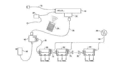
101520253035WO 98/09268CA 02264609 1999-02-26PCT/US97/15170TRANSPORTABLE ELECTROLUMINESCENT DISPLAY SYSTEMThis application claims the benefit of U.S.Provisional Application No. 60/024,807, filed August28, 1996, which is incorporated herein by reference.BACKGROUND OF THE INVENTIONField of the InventionThe present invention relates to an electronicdisplay system and circuitry for controlling thedisplay. In particular, the invention relates to adisplay system employing an arrangement ofelectroluminescent pixels for displaying alphanumericsymbols or other characters and electronic circuitryfor their control.Description of the Related ArtConventional display systems employ matrixes ofeither incandescent bulbs (see, for example, U.S.patents 3,941,926 and 4,148,073 to Slobodzian et al.)or lightâemitting diodes (see, for example, U.S.patent 4,323,896 to Fiedler et al.) to displayalpha-numeric symbols, characters or pictorialrepresentations. In such display systems, individualbulbs or lightâemitting diodes are typically arrangedin a matrix of horizontal rows and vertical columnsand the matrix is connected to electronic circuitrythat serves to activate individual bulbs or diodes.The circuitry selectively controls the activation ofan appropriate combination of individual bulbs ordiodes to create the desired alpha-numeric, character101520253035WO 98/09268CA 02264609 1999-02-26PCT/US97/ 15170-2-or pictorial image. Through the proper selection andtiming of bulb or diode activation, images ormessages which appear to scroll across the displaysystem can be created.There are significant drawbacks associated withdisplay systems based on incandescent lamps, namelytheir fragility, consumption of significant amountsof electrical power, excessive bulk and weight.Light emitting diode (LED) based display systems arealso bulky and heavy, as well as being limited insize. The excessive bulk and weight of these boardsrestrict their transportability and usability inapplications requiring large scale displays. Inaddition, both incandescent and light-emitting diode-based display systems are rigid, thereby precludingtheir use on curved or irregular shaped surfaces.Electroluminescent lamps employing phosphorsthat luminesce when subjected to electric fields areknown. Until now, the use of electroluminescentlights has, however, been limited to single light"strips" which require the additional use ofpatterned sleeves for the display of predeterminedmessages (see U.S. patent 5,566,384 to Chien).Still needed in the field is a display systemthat is light weight, small in size, low in powerconsumption, scalable, and flexible, and thereforecan be easily transported and used on any shapedsurfaces.SUMMARY OF THE INVENTIONThe present invention provides a display system which includes an electroluminescent display unitwith a plurality of electroluminescent pixels, areceiver for receiving a signal that containsinformation regarding an image to be displayed on the10l520253035WO 98109268CA 02264609 1999-02-26PCT/US97/15170-3-unit, a signal processor for processing theinformation contained in the signal and means forproviding the processed signal to theelectroluminescent display so as to activate selectedpixels of the plurality of electroluminescent pixelsin order to display the image.The invention also provides anelectroluminescent display system which includes anelectroluminescent display unit with a plurality ofelectroluminescent pixels, a signal source forproviding a signal that contains informationregarding an image to be displayed on the unit, atransmitter for gathering the signal from the source,a receiver for receiving the signal from thetransmitter, a signal processor for processing theinformation contained in the signal and means forproviding the processed signal to theelectroluminescent display so as to activate selectedpixels of the plurality of electroluminescent pixelsto display the image.The invention also provides the systems asdescribed above wherein the display includes aplurality of panels and each of the plurality ofpanels has a matrix of electroluminescent pixelsarranged in horizontal rows and vertical columns.A better understanding of the features andadvantages of the present invention will be obtainedby reference to the following detailed descriptionand accompanying drawings which set forthillustrative embodiments in which the principles ofthe invention are utilized.BRIEE D§§CRIPTION OF THE DRAWIN§_§FIG. 1 is a block diagram illustrating anembodiment of the invention.101520253035WO 98/09268CA 02264609 1999-02-26PCT/US97I15l70_4_FIG. 2 is circuit diagram of a transmitter of anembodiment of the invention.FIG. 3 is circuit diagram of a receiver of anembodiment of the invention.FIG. 4 is a block diagram of a processor of anembodiment of the invention.FIG. 5 is a circuit diagram of a pixel selectorof an embodiment of the invention.Fig. 6 is a circuit diagram of a panel drivingmodule of an embodiment of the invention.Fig. 7 is a circuit diagram of a buffer cable ofan embodiment of the invention.DETAILED DESCRIPTION OFâ THE PREFERRED EMBODIMENTSElectroluminescent lamps are lightweight comparedto other light sources, can be printed on flexibleclothâlike substrates and may be fabricated in a flatand thin configuration. They also consume less powerthan incandescent bulbs. These characteristics ofelectroluminescent lamps provide several benefits inthe present inventive electroluminescent displaysystem, including (i) a display system that can beapplied and conformed to irregular or curved surfaces,(ii) a display system that can be easily transportedon lighterâthan-air craft, (iii) a display system thatcan be scaled to any desired size, (iv) a displaysystem that can be supported by a structure withlimited load bearing capability, (V) a display systemthat is very thin and (vi) a display system thatconsumes a relatively small amount of power per unitof light emitting area as compared to other displaylight systems.A typical example electroluminescent panel,according to the present invention, having a 5x7matrix of 2" round pixels is 14" X 20â in size andweighs on an average 0.422 g/inâ. Such an example101520253035WO 98/09268CA 02264609 1999-02-26PCT/US97l15170-5-panel will typically provide more than 10 footlamberts of light per square inch of light emittingsurface while operating at 1200 hertz, 90 volts, and.5 to 1.5 milliamps per square inch of light emittingsurface. Thus, an example sixteen panel display wouldonly draw from approximately 160 to 500 milliamps ofcurrent depending on the number of pixels that arelit. This example demonstrates that much larger andbrighter panels can be constructed well within theoperating capabilities of electroluminescent lamps.Electroluminescent lamps are described in moredetail in the following applications, all of which arefully incorporated herein by reference:(1) application No. 08/591,014, filed January 25,1996; (2) application No. 08/698,973, filed August16, 1996; (3) application No. 08/783,732, filedJanuary 16, 1997; and (4) application titled"Electroluminescent Lamp Design" by inventors Bryan D.Haynes, Michael C. Feldman and Matthew C. Wllkinson,filed August 13, 1996 (Attorney Docket Number AVI-140).Turning to Fig. 1, an embodiment of the presentIn theembodiment pictured, the display system includesinvention is depicted in a block diagram.driver circuitry that receives display informationsignals from a miniature scrolling board 10. Acommercially available miniature scrolling board 10that could be used is Model No. PL-M2012R TruâColorII, manufactured by ProâLite Inc. of Santa Ana,California. It will be understood by one skilled inthe art that any miniature scrolling board 10 can beused to provide display information signaling andfurther, the invention can be implemented without theuse of a miniature scrolling board at all. Instead, apersonal computer or other information signalgenerating device can be used.101520253035WO 98109268CA 02264609 1999-02-26PCT/U S97/ 15170-5-The miniature scrolling board 10 shown in Fig. 1provides for two different alternative displayinformation input sources. First, via line 15, apersonal computer or other data processing device canbe coupled to the miniature scrolling board 10 toprovide display information to the display system.Second, via a remote control keypad 25 and a remotecontrol signal receiver (not pictured) within theminiature scrolling board 10, display information canbe sent to the display system. The miniaturescrolling board 10 receives power via power supply 20which is connected to a power source such as aconventional wall outlet or in transportableapplications; battery or generator systems.Fig. 1 further depicts a transmitter 30 coupledto the miniature scrolling sign 10. The transmitter30 transmits the display information signaling fromthe miniature scrolling sign 10 to a receiver 40 viatransmission line 35. The receiver 40 is coupled tothe first of a series of daisyâchained informationsignal processing modules 55, 60, 65 by line 45. Theinformation signal processing modules 55, 60, 65 arelinked together via connector lines 70, 75, 80. Inother words, the information signal processing modules55, 60, 65 and the connector lines 70, 75, 80 form adata bus that carries the display informationsignaling to each information signal processing module55, 60, 65.The information signal processing modules 55,_60,65 interpret the display information signalingtraveling along the data bus which is sent from theminiature scrolling sign 10 via the transmitter 30 andreceiver 40. Based on the display informationsignaling, the information signal processing modules55, 60, 65 control which electroluminescent segments(or pixels) of an electroluminescent panel associated101520253035WO 98/09268CA 02264609 1999-02-26PCTIUS97/15170-7-with the particular information signal processingmodule 55, 60, 65 are to be illuminated by allowingpower to flow from an alternating current power supply85. In other words, the information signal processingmodules 55, 60, 65 act as gates (or switches),controlled by the display information signal tocontrol the flow of AC electricity to theelectroluminescent segments.While the connector lines 70, 75, 80 arerelatively short in the pictured embodiment, thedistance between the modules and the total number ofmodules can be increased by installing a buffer cable(see Fig. 7) between the modules in place of theexisting connector line. The buffer cable amplifiesthe signal to overcome any attenuation caused by theextended length of the conductor.Each information signal processing module 55, 60,65 is also connected in parallel to an alternatingcurrent power source 85 via power line 90. The powerline 90 is further branched within each informationsignal processing module 55, 60, 65 to provideswitched power to each distinct segment of the signalprocessing module's associated electroluminescentpanel (not shown).The particular embodiment shown in Fig. 1 isdesigned to work with electroluminescent display unitswhich include 16 electroluminescent panels with eachpanel having an XâY matrix of electroluminescentpixels. While the panel for use with the Fig. 1embodiment of the invention uses a 5x7 matrix ofpixels, any size XâY matrix or other arrangement ofelectroluminescent segments can be used according tothe invention. The number of panels, panel size,number of pixels, pixel size, and pixel arrangementwill depend on the conditions under which the board isused, e.g. viewing distance, light conditions,101520253035WO 98/09268CA 02264609 1999-02-26PCT/US97/15170-9-required image resolution, etc. Further, theindividual electroluminescent segments may be of anyshape or size and, in order to make larger individualpixels, separate electroluminescent lamps may beconnected.Turning now to Fig. 2, a circuit diagram of anembodiment of the transmitter 30 is shown. Jumperblock J130 is connected to the internal circuitry ofthe miniature scrolling board 10 and provides accessto the display information signals within theminiature scrolling board 10. The particular signalsof the disclosed embodiment include three row selectdisplay information signals that can be decoded toindicate which of the seven rows include a segment orpixel that will be illuminated and two column selectdisplay information signals that can be decoded toindicate which of the five columns include a segmentor pixel that will be illuminated. The transmitter 30includes an optical isolation circuit U102, U103, U104connected to the jumper block J130 which insulates therest of the system from the potential damage caused byelectrical spikes. The transmitter also includes linedrivers U105 and U106 connected to the output of theoptical isolation circuit U102, U103, U104 that bufferthe signals and output them on the transmission line35 to the receiver 40.Figure 3 shows a circuit diagram of acorresponding embodiment of the receiver 40. Thereceiver 40 includes a pass-through line driver U202that buffers the row select signals ROWSELA, ROWSELB,ROWSELC and feeds them into the data bus. The twocolumn select signals include a clock signal CLOCK anddata signal DATA.data signal is a serial bit stream indicating theIn this particular embodiment, thedesired state of adjacent pixels in a given row.To correct any signal skew after transmission,101520253035WO 98/09268CA 02264609 1999-02-26PCT/US97/15170-9-the clock signal is passed through a skew adjustmentcircuit U203B before the column select signals arepassed to the line driver U202 and then fed to thedata bus.Fig. 4 is a more detailed block diagram of aninformation signal processing module 55. Recall thateach information signal processing module 55 has acorresponding electroluminescent panel that it drives.Note that all of the information signal processingmodules 55, 60, 65 are identical to each other andfunction in the same way. Thus, it should beunderstood that the following description regardinginformation signal processing module 55 applies to theother information signal processing modules as well.Referring to both Figs. 1 and 4, the data bus 105is depicted as spanning across the information signalprocessing module 55 where the left end of the databus 105 is connected to the output of the receiver 40via line 45 and the right end of the data bus isconnected to the next information signal processingmodule 60 via a connector line 70.The information signal processing module 55includes a pixel selector 120 and a gate array 150,155, 160, 165, 170 for each column of pixels in the5x7 matrix. The pixel selector 120 includes a columnsselector 140 and a rows selector 145. The pixelselector 120 receives the three row selection displayinformation signals from the data bus 105 via lines125, 130, 135. The pixel selector 120 receives thetwo column selection display information signals fromthe data bus 105 via lines 110 and 115.Turning to Fig. 5, an embodiment a circuitimplementing the pixel selector is shown. The rowsselector 145 in this embodiment is a three to eightdecoder U17 while the columns selector 140 is an eightbit serial to parallel converter/shift register U16.l01520253035WO 98/09268CA 02264609 1999-02-26PCT/US97/15170-10..The three to eight decoder U17 takes the three rowselection display information signals from the databus 105 as inputs and activates the appropriate ROWsignals as outputs.The eight bit serial to parallel converter/shiftregister U16 takes the two column selection displayinformation signals from the data bus 105 as inputs,shifts the data though, and activates the appropriateCOL signals as outputs. The last output is also sentback to the data bus to the next module. As with thethree to eight decoder U17, the eight bit serial toparallel converter U16 has more capacity thannecessary for a five column pixel matrix.Referring again to Fig. 4, at this point, thecorrect state of each pixel in the 5x7 grid can bedetermined by logically combining together eachcolumns selector 140 output with each rows selectoroutput as indicated by the gate array blocks 150, 155,160, 165, 170. Each gate in the gate array blocks150, 155, 160, 165, 170 has an associated pixel on thepanel. Essentially, each row and column pair controlsa switch, that when closed, allows power to flow fromthe AC power supply 175, over the power line 180, andthrough the gate to charge the corresponding pixel.Turning to Fig. 6, a circuit diagram of anembodiment of the gate array 150 of Fig. 4 is shown.Row and column signals are combined together using ANDgates U1, U2. If the result of the ANDing is that thepixel is to be illuminated, a brief pulse is output tothe RC circuit RN1, C4. Component values are selectedsuch that the pulse causes the capacitor CR4 to chargeup and hold a voltage level for a predetermined time.The effect is to convert the pulse out of the OR gateU1 into a level signal that switches the transistor Q1for the desired amount of time such that sufficientalternating current from the power supply 175 flows to101520WO 98/09268CA 02264609 1999-02-26PCT/US97l15170-11-the electroluminescent pixel to light it for thedesired amount of time.Fig. 7 depicts an embodiment of a buffer cablecircuit used to re-amplify the column selectiondisplay information signal when it is desired to havemany information signal processing modules 55, 60, 65daisy chained together or the distances between themodules 55, 60, 65 is large. A buffer cable as shownin Fig. 7 can be used in place of a connection line70, 75, 80 as needed.In another embodiment, the electroluminescentpixels are fabricated on a flexible substrate asdescribed in provisional application No. 60/023,923,filed August 13, 1996, which is incorporated herein byreference.It should be understood that various alternativesto the embodiments of the invention described hereinmay be employed in practicing the invention. It isintended that the following claims define the scope ofthe invention and that structures within the scope ofthese claim and their equivalents by covered thereby.