Language selection

Search

Patent 2273223 Summary

Third-party information liability

Some of the information on this Web page has been provided by external sources. The Government of Canada is not responsible for the accuracy, reliability or currency of the information supplied by external sources. Users wishing to rely upon this information should consult directly with the source of the information. Content provided by external sources is not subject to official languages, privacy and accessibility requirements.

Claims and Abstract availability

Any discrepancies in the text and image of the Claims and Abstract are due to differing posting times. Text of the Claims and Abstract are posted:

  • At the time the application is open to public inspection;
  • At the time of issue of the patent (grant).
(12) Patent: (11) CA 2273223
(54) English Title: CHIP-SIZE PACKAGE USING A POLYIMIDE PCB INTERPOSER
(54) French Title: BOITIER DE CIRCUIT INTEGRE DE LA TAILLE D'UNE PUCE UTILISANT UN INTERPOSEUR DE CARTE DE CIRCUIT IMPRIME EN POLYIMIDE
Status: Expired
Bibliographic Data
(51) International Patent Classification (IPC):
  • H01L 23/498 (2006.01)
(72) Inventors :
  • WARREN, ROBERT W. (United States of America)
(73) Owners :
  • RAYTHEON COMPANY (United States of America)
(71) Applicants :
  • RAYTHEON COMPANY (United States of America)
(74) Agent: SIM & MCBURNEY
(74) Associate agent:
(45) Issued: 2003-11-11
(86) PCT Filing Date: 1998-09-29
(87) Open to Public Inspection: 1999-04-08
Examination requested: 1999-05-28
Availability of licence: N/A
(25) Language of filing: English

Patent Cooperation Treaty (PCT): Yes
(86) PCT Filing Number: PCT/US1998/020467
(87) International Publication Number: WO1999/017364
(85) National Entry: 1999-05-28

(30) Application Priority Data:
Application No. Country/Territory Date
08/939,832 United States of America 1997-09-29

Abstracts

English Abstract


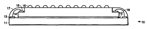
A chip-size package formed using a printed circuit board, preferably
comprising polyimide. The chip-size package comprises an integrated circuit
chip having a plurality of peripheral bond pads. The printed circuit board has
a plurality of solder bumps formed on its top surface and a plurality of bond
pads around its periphery. A layer of adhesive is used to secure the printed
circuit board and the integrated circuit chip together. A plurality of wire
bonds electrically connected between selected bond pads of the integrated
circuit chip and the printed circuit board. An encapsulant encapsulates the
wire bonds and bond pads of the integrated circuit chip and the printed
circuit board.


French Abstract

La présente invention concerne un boîtier de la taille d'une puce formé à l'aide d'une carte de circuit imprimé comprenant de préférence un polyimide. Ce boîtier de la taille d'une puce comprend une puce de circuit intégré possédant plusieurs plages de connexion périphériques. La carte de circuit imprimé comprend plusieurs perles de soudure formées sur sa surface supérieure et plusieurs plages de connexion autour de sa périphérie. On utilise une couche d'adhésif pour fixer mutuellement la carte de circuit imprimé et la puce de circuit imprimé. Plusieurs connexions de fils sont électriquement reliées entre des plages de connexion sélectionnées de la puce de circuit intégré et la carte de circuit intégré. Un organe d'enrobage encapsule les connexions de fils et les plages de connexion de la puce de circuit intégré et de la carte de circuit intégré.

Claims

Note: Claims are shown in the official language in which they were submitted.


5

CLAIMS

What is Claimed is:

1. A chip-size integrated circuit package comprising:
an integrated circuit chip having a plurality of peripheral bond pads;

a polyimide printed circuit board having a plurality of solder bumps formed on
a
top surface thereof and a plurality of bond pads around its periphery;

a layer of adhesive disposed between the polyimide printed circuit board and
the
integrated circuit chip to secure them directly together;

a plurality of wire bonds electrically connected between selected bond pads of
the
integrated circuit chip and the polyimide printed circuit board; and

an encapsulant for encapsulating the wire bonds and bond pads of the
integrated
circuit chip and the polyimide printed circuit board.

2. The package of claim 1 wherein the integrated circuit chip comprises a
silicon integrated circuit chip.

3. The package of claim 1 wherein the layer of adhesive comprises a layer of
epoxy adhesive.

4. The package of claim 1 wherein the encapsulant comprises flexible epoxy.

5. The package of claim 1 wherein the encapsulant comprises silicone.


Description

Note: Descriptions are shown in the official language in which they were submitted.


CA 02273223 2002-10-10
CHIP-SIZE PACKAGE USING A POLYIMIDE PCB INTERPOSER
BACKGROUND
The present invention relates generally to integrated circuit packages and
methods, and more particularly, to a chip-size integrated circuit package
formed using a
polyimide printed circuit board interposer.
The closest form of art to the present invention is a chip-size package made
by a
company called Tessera. The Tessera chip-size package uses formed tape
automated
bonded (TAB) lead frames on a polyimide film. It would be desirable to have a
chip-size
package that has fewer processing steps, is less expensive to build, and that
employs
commonly available processing equipment.
Furthermore, most chip size package designs are larger than the die itself. It
would therefore be desirable to have a chip-size package that packages the
integrated
circuit chip within the internal surface area of the bare die.
Accordingly, it is an objective of the present invention to provide for an
improved
chip-size package formed using a polyimide printed circuit board interposer.
SUMMARY OF THE INVENTION
To meet the above and other objectives, the present invention provides for a
chip-
size package formed using a polyimide printed circuit board interposer. In
accordance
with one aspect of the present invention there is provided a chip-size
integrated circuit
package comprising:
an integrated circuit chip having a plurality of peripheral bond pads;
a polyimide printed circuit board having a plurality of solder bumps formed on
a
top surface thereof and a plurality of bond pads around its periphery;
a layer of adhesive disposed between the polyimide printed circuit board and
the
integrated circuit chip to secure them directly together;
a plurality of wire bonds electrically connected between selected bond pads of
the
integrated circuit chip and the polyimide printed circuit board; and
an encapsulant for encapsulating the wire bonds and bond pads of the
integrated
circuit chip and the polyimide printed circuit board.
It is believed that the present invention may be built for a lower cost than
the
Tessera or other prior art chip-size package because the present invention has
fewer
processing steps and has a lower material cost. The present invention also
uses more
common and lower cost processing equipment than does the Tessera or other
prior art
process.

CA 02273223 1999-OS-28
WO 99/17364 " PCT/US98/20467
The present invention converts a single, unpackaged bare silicon chip into a
packaged chip no larger in area than the bare chip. 'the present invention
uses readily
available printed circuit board materials and technology. This chip size
packaging
scheme of the present invention is novel in that it uses a low cost printed
circuit board
interposes with exposed. lower layers incorporating wire bond pads. The wire
bond
pads are sufficiently lower than the solder bumps on the cog layer of the
interposes. and
as such. wire bonds to the wire bond pads can be encapsulated without
exceeding the
height of the top printed circuit board layer which rnust remain flat for
soldering.
The present invention converts a bare chip into a chip size package. The chip
size package may be assembled in a manner similar to surface mount devices
which are
soldered to printed ciccuit boards. Chip size packages, however, take up only
10-20%
of the area of conventionally packaged chips fabricated as surface mount
devices.
Development of the chip size package of the present invention is an important
step in
achieving miniaturization of microelectronics.
Most chip size packages are lamer than the; die itself. The present invention
however, packages the chip within the internal surface area of the bare die.
Because the
present chip size package takes up no additional area than the bare die, it is
believed to
be the smallest two-dimensional integrated circuit package that has yet been
developed.
The oenefit of converting a bare die into a surface mount device is chat it
provides mechanical and environmental protection for the fragile silicon
integrated
circuit chip. The present invention also converts a fine pitch peripheral pad
integrated
circuit into a packaged. courser pitch area array device. permitting it to be
easily tested.
burned in, and assembled to standard printed circuit boards using existing.
common
equipment used in the industry. The ability to us,e "known good" tested
devices while
utilizing industry standard and accepted equipment and processes is a key
element in
obtaining the absolute lowest product cost.
The present invention permits silicon integrated circuiu to be packaged in the
smallest area possible. which is no larger than the size of the integrated
circuit itself.
Incorporating such low cost integrated circuit packages into various
microelectronic
applications will provide for smaller product sizes, lower weight, and lower
assembly
and testing costs. The present invention provides for a robust packaging
structure that
is suitable for a variety of commercial and milit~uy applications. including
automotive
electronics, for example.
BRIEF DESCRIPTION OF THE DRAWINGS
The various features and advantages of the present invention may be more
readily understood with reference to the following detailed description taken
in

CA 02273223 1999-OS-28
WO 99117364 " PCT/US98/20467
3
conjunction with the accompanying drawings, wherein Iike reference numerals
represent like structural elements. and in which:
Fig. 1a-lc illustrate formation of a chip-size; integrated circuit packase in
accordance with the principles of the present inventuon:
Fig. 2 is a perspective view of a fully assembled chip-size integrated circuit
package; and
Fig. 3 illustrates the chip-size integrated circuit package assembled to a
printed
circuit board.
DETrIILED DESCRIP'CION
Referring to the drawing figures. Fig. la-lc illustrate formation of a chip-
size
integrated circuit package 10 in accordance with tb~e principles of the
present invention.
Referring to Fib. la, the chip-size integrated circuit package LO comprises an
integrated
circuit chip 11, which may be a silicon integrated circuit chip 11. for
example, having a
plurality of peripheral bond pads 13. A printed circuit board 14, or
interposer 14.
which is preferably comprised of polyimide. is formed having a plurality of
solder
bumps 16 (or an area array of solder bumps 16) formed on a top surface. and a
plurality
of bond pads 15 around its periphery. The polyirnide printed circuit board 14,
or
interposer 14. is attached to the integrated circuit chip 11 using a layer of
adhesive 12.
such as a layer of epoxy adhesive 12. for example.
Fig. 1b shows an assembled chip-size package 10 wherein the polyimide
printed circuit board 14 is electrically attached to the integrated circuit
chip 1 t using a
plurality of wire bonds 18 coupled between the respective pluralities of bond
pads 13.
15. Referring to Fig. 1 c. after the wire bonds 18 are formed between the
polyimide
printed circuit board 14 and the integrated circuit chip I 1. the wire bonds
18 are
encapsulated using an encapsulant 17, such as flexible epoxy or silicone, for
example.
Fig. 2 is a perspective view of a fully assembled chip-size integrated circuit
package 10. The encapsulant 17 is shown in ph,uttom. The chip-size integrated
circuit
package 10 has the area array of solder bumps 16 exposed for reflow soldering.
Fig. 3 illustrates the chip-size integrated circuit package 10 of Fig. 2
assembled
to a printed circuit board 21. The printed circuit board 21 has an area array
of solder
bumps 22 that matches the area array of solder bumps 16 on the chip-size
integrated
circuit package 10. The chip-size integrated circuit package 10 and the
printed circuit
board 21 are electrically connected together by reflowing the solder bumps 16.
22 to
form the electrical interconnections therebetween.
Thus, the present invention provides for a chip-size package 10 formed using a
polyimide printed circuit board interposer 14. Lt is believed that the present
invention

CA 02273223 1999-OS-28
WO 99/17364 PCT/US98/20467
may be built for a relatively low cost than prior art chip-size packages
because the
present invention has fewer processing steps and has lower material costs. The
present
invention also uses more common and lower cost processing equipment than is
used to
produce prior art chip-size packages.
The present invention converts a single, unpackaged bare integrated circuit
chip
11, for example, into a packaged chip 20 no larger in area than the bare chip
1 I. The
present invention uses readily available printed cirt:uit board materials and
technology.
The chip size package 10 uses the low cost printed circuit board interposer l4
with
exposed, lower layers having wire bond pads 13, 15. The wire bond pads 13. I5
are
sufficiently lower than the solder bumps 16 on top of the interposer i4, and
therefore,
wire bonds 18 to the wire bond pads 13, 15 are encapsulated without exceeding
the
height of the top printed circuit board 14 which must remain flat for
soldering.
The present invention thus converts a bare chip 11 into a chip size package
I0.
The chip size package 10 may be assembled in a manner similar to surface mount
devices which are soldered to printed circuit boards. The chip size package
10.
however, takes up only 10-20% of the area of conventionally packaged chips 11
fabricated as surface mount devices.
The present invention packages the chip L :l within the internal surface area
of
the bare chip 11. Because the chip size package 1~0 takes up no additional
area than the
bare chip 11, it is believed to be the smallest two-dimensional integrated
circuit package
10 that has yet been developed.
The chip size package LO provides mecharucal and environmental protection for
the fragile integrated circuit chip 1 I . The chip size package 10 also
converts a fine pitch
peripheral pad integrated circuit 11 into a packaged, courser pitch area array
device.
permitting it to be easily tested, burned in, and assembled to standard
printed circuit
boards 21 ustng existing, common equipment used in the industry.
The present invention permits integrated circuits to be packaged in the
smallest
area possible, which is no larger than area of the integrated circuit 11. The
chip size
package 10 provides for a robust packaging structure that is suitable for a
variety of
commercial and military applications, including automotive electronics, for
example.
Thus, a chip-size package formed using a polyimide printed circuit board
intetposer has been disclosed. It is to be understood that the described
embodiment is
merely illustrative of some of the many specific embodiments which represent
applications of the principles of the present invention. Clearly, numerous and
other
arrangements can be readily devised by those skililed in the art without
departing from
the scope of the invention.

Representative Drawing
A single figure which represents the drawing illustrating the invention.
Administrative Status

For a clearer understanding of the status of the application/patent presented on this page, the site Disclaimer , as well as the definitions for Patent , Administrative Status , Maintenance Fee  and Payment History  should be consulted.

Administrative Status

Title Date
Forecasted Issue Date 2003-11-11
(86) PCT Filing Date 1998-09-29
(87) PCT Publication Date 1999-04-08
(85) National Entry 1999-05-28
Examination Requested 1999-05-28
(45) Issued 2003-11-11
Expired 2018-10-01

Abandonment History

There is no abandonment history.

Payment History

Fee Type Anniversary Year Due Date Amount Paid Paid Date
Request for Examination $400.00 1999-05-28
Registration of a document - section 124 $100.00 1999-05-28
Application Fee $300.00 1999-05-28
Registration of a document - section 124 $100.00 1999-09-23
Maintenance Fee - Application - New Act 2 2000-09-29 $100.00 2000-08-22
Maintenance Fee - Application - New Act 3 2001-10-01 $100.00 2001-08-23
Maintenance Fee - Application - New Act 4 2002-09-30 $100.00 2002-08-16
Final Fee $300.00 2003-08-12
Maintenance Fee - Application - New Act 5 2003-09-29 $150.00 2003-08-14
Maintenance Fee - Patent - New Act 6 2004-09-29 $200.00 2004-08-16
Maintenance Fee - Patent - New Act 7 2005-09-29 $200.00 2005-08-17
Maintenance Fee - Patent - New Act 8 2006-09-29 $200.00 2006-08-17
Maintenance Fee - Patent - New Act 9 2007-10-01 $200.00 2007-08-15
Maintenance Fee - Patent - New Act 10 2008-09-29 $250.00 2008-08-13
Maintenance Fee - Patent - New Act 11 2009-09-29 $250.00 2009-09-17
Maintenance Fee - Patent - New Act 12 2010-09-29 $250.00 2010-08-23
Maintenance Fee - Patent - New Act 13 2011-09-29 $250.00 2011-09-06
Maintenance Fee - Patent - New Act 14 2012-10-01 $250.00 2012-08-08
Maintenance Fee - Patent - New Act 15 2013-09-30 $450.00 2013-08-14
Maintenance Fee - Patent - New Act 16 2014-09-29 $450.00 2014-09-04
Maintenance Fee - Patent - New Act 17 2015-09-29 $450.00 2015-09-09
Maintenance Fee - Patent - New Act 18 2016-09-29 $450.00 2016-09-08
Maintenance Fee - Patent - New Act 19 2017-09-29 $450.00 2017-09-06
Owners on Record

Note: Records showing the ownership history in alphabetical order.

Current Owners on Record
RAYTHEON COMPANY
Past Owners on Record
HUGHES ELECTRONICS
WARREN, ROBERT W.
Past Owners that do not appear in the "Owners on Record" listing will appear in other documentation within the application.
Documents

To view selected files, please enter reCAPTCHA code :


To view images, click a link in the Document Description column. To download the documents, select one or more checkboxes in the first column and then click the "Download Selected in PDF format (Zip Archive)" or the "Download Selected as Single PDF" button.

List of published and non-published patent-specific documents on the CPD .

If you have any difficulty accessing content, you can call the Client Service Centre at 1-866-997-1936 or send them an e-mail at CIPO Client Service Centre.


Document
Description 
Date
(yyyy-mm-dd) 
Number of pages   Size of Image (KB) 
Drawings 1999-05-28 2 46
Claims 1999-05-28 1 25
Representative Drawing 1999-08-19 1 3
Representative Drawing 2003-10-08 1 3
Cover Page 2003-10-08 1 37
Abstract 1999-05-28 1 38
Description 1999-05-28 4 197
Cover Page 1999-08-19 1 46
Description 2002-10-10 4 220
Claims 2002-10-10 1 26
Assignment 1999-05-28 3 117
PCT 1999-05-28 3 97
Correspondence 1999-07-13 1 31
Assignment 1999-09-23 8 387
Prosecution-Amendment 1999-11-02 3 93
Prosecution-Amendment 2002-06-10 2 46
Prosecution-Amendment 2002-10-10 5 194
Correspondence 2003-08-12 1 50