Note: Descriptions are shown in the official language in which they were submitted.
CA 02280174 1999-08-OS
WO 98135408 PCT/US98/00725
HIGH SPEED, HIGH DENSITY ELECTRICAL CONNECTOR
This invention relates generally to electrical
connectors used to interconnect printed circuit boards and
more specifically to a method of simplifying the
manufacture of such connectors.
Electrical connectors are used in many electronic
systems. It is generally easier and more cost effective to
manufacture a system on several printed circuit boards
which are then joined together with electrical connectors.
A traditional arrangement for joining several printed
circuit boards is to have one printed circuit board serve
as a backplane. Other printed circuit boards, called
daughter boards, are connected through the backplane.
A traditional backplane is a printed circuit board
with many connectors. Conducting traces in the printed
circuit board connect to signal pins in the connectors so
that signals may be routed between the connectors. Other
printed circuit boards, called "daughter boards" also
contain connectors that are plugged into the connectors on
the backplane. In this way, signals are routed among the
daughter boards through the backplane. The daughter cards
often plug into the backplane at a right angle. The
connectors used for these applications contain a right
angle bend and are often called "right angle connectors."
Connectors are also used in other configurations for
interconnecting printed circuit boards, and even for
connecting cables to printed circuit boards. Sometimes,
one or more small printed circuit boards are connected to
another larger printed circuit board. The larger printed
circuit board is called a "mother board" and the printed
circuit boards plugged into it are called daughter boards.
Also, boards of the same size are sometimes aligned in
parallel. Connectors used in these applications are
sometimes called "stacking connectors" or "mezzanine
. 35 connectors."
CA 02280174 1999-08-OS
WO 98/354 PCT/US98/00725
Regardless of the exact application, electrical
connector designs have generally needed to mirror trends in
the electronics industry. Electronic systems generally
have gotten smaller and faster. They also handle much more
data than systems built just a few years ago. To meet the
changing needs of these electronic systems, some electrical
connectors include shield members. Depending on their
configuration, the shields might control impedance or
reduce cross talk so that the signal contacts can be placed
closer together.
An early use of shielding is shown in Japanese patent
disclosure 49-6543 by Fujitsu, Ltd. dated February 15,
1974. US patents 4,632,476 and 4,806,107 - both assigned
to AT&T Bell Laboratories - show connector designs in which
shields are used between columns of signal contacts. These
patents describe connectors in which the shields run
parallel to the signal contacts through both the daughter
board and the backplane connectors. Cantilevered beams are
used to make electrical contact between the shield and the
backplane connectors. Patents 5,433,617; 5,429,521;
5,429,520 and 5,433,618 - all assigned to Framatome
Connectors International - show a similar arrangement. The
electrical connection between the backplane and shield is,
however, made with a spring type contact.
Other connectors have the shield plate within only the
daughter card connector. Examples of such connector
designs can be found in patents 4,846,727; 4,975,084;
5,496,183; 5,066,236 - all assigned to AMP, Inc. An other
connector with shields only within the daughter board
connector is shown in US patent 5,484,310, assigned to
Teradyne, Inc.
Another modification made to connectors to accomodate
changing requirements is that connectors must be much
larger. In general, increasing the size of a connector
means that manufacturing tolerances must be much tighter.
The permissible mismatch between the pins in one half of
- 2 -
CA 02280174 1999-08-OS
WO 98/35408 PCT/ITS98/00725
the connector and the receptacles in the other is constant,
regardless of the size of the connector. However, this
constant mismatch, or tolerance, becomes a decreasing
percentage of the connector's overall length as the
' 5 connector gets larger. Therefore, manufacturing tolerances
must be tighter for larger connectors, which can increase
' manufacturing costs. One way to avoid this problem is to
use modular connectors. Teradyne Connection Systems of
Nashua, New Hampshire, USA pioneered a modular connector
system called HD+~, with the modules organized on a
stiffener. Each module had multiple columns of signal
contacts, such as 15 or 20 columns. The modules were held
together on a metal stiffener.
An other modular connector system is shown in US
Patents 5,066,236 and 5,496,183. Those patents describe
"module terminals" with a single column of signal contacts.
The module ternlinals are held in place in a plastic housing
module. The plastic housing modules are held together with
a one-piece metal shield member. Shields could be placed
between the module terminals as well.
It would be highly desirable if a modular connector
could be made with an improved shielding configuration. It
would also be desirable if the manufacturing operation were
simplified. It would be further desirable if a design
could be developed that allowed easy intermixing of single
ended and differential signal contacts.
- 3 -
CA 02280174 1999-08-OS
wo 9sr~s4os rcTrtrs9sioo~zs _ _
SUN~iARY OF THE INVENTION
With the foregoing background in mind, it is an object
of the invention to provide a high speed, high density
connector.
It is a further object to provide a modular connector
that is easy to manufacture.
It is a further object to provide a low insertion
force connector.
It is also an object to provide a connector that can
be easily assmebled to include signal contacts configured
for single end or differential signals.
The foregoing and other objects are achieved in an
electrical connector manufactured from a plurality of
wafers. Each wafer is made with a ground plane insert
molded into a housing. The housing has cavities into which
signal contacts are inserted.
In a preferred embodiment, the signal contacts are
also insert molded into a second housing piece. The two
housing pieces snap together to form one wafer. The wafers
are held together on a metal stiffener.
- 4 -
CA 02280174 1999-08-OS
wo ~3s4os rcTrtrs9sroons
BRIEF DESCRIPTION OF THE DRAWINGS
The invention will be better understood by reference
to the following more detailed description and accompanying
drawings in which
FIG. 1 is an exploded view of a connector made in
accordance with the invention;
FIG. 2 is a shield plate blank used in the connector
of FIG. 1;
FIG. 3 is a view of the shield plate blank of FIG. 2
after it is insert molded into a housing element;
FIG. 4 is a signal contact blank used in the connector
of FIG. 1;
FIG. 5 is a view of the signal contact blank of FIG. 4
after it is insert molded into a housing element;
FIG. 6 is an alternative embodiment of the signal
contact blank of FIG. 4 suitable for use in
making a differential module;
FIGS. 7A-7C are operational views a prior art
connector;
FIGS. 8A-8C are similar operational views of the
connector of FIG. 1;
FIG. 9A and 9B are backplane hole and signal trace
patterns for single ended and differential
embodiments of the invention, respectively; and
FIG. 10 is a view of an alternative embodiment of the
invention.
FIG. 11A is a an alternative embodiment for the plate
128 in FIG. 1;
FIG. 11B is a cross sectional view taken through the
line B-B of FIG. 11A;
FIG. 12 is an isometric view of a connector according
to the invention.
- 5 -
CA 02280174 1999-08-OS
WO 98/35408 PCT/US98/00725
DESCRIPTION OF THE PREFERRED EMBODIMENT
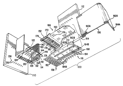
FIG. 1 shows an exploded view of backplane assembly
100. Backplane 110 has pin header 114 attached to it.
Daughter card 112 has daughter card connector 116 attached
to it. Daughter card connector 116 can be mated to pin
header 114 to form a connector. Backplane assembly likely
has many other pin headers attached to it so that multiple
daughter cards can be connected to it. Additionally,
multiple pin headers might be aligned end to end so that
multiple pin headers are used to connect to one daughter
card. However, for clarity, only a portion of backplane
assembly and a single daughter card 112 are shown.
Pin header 114 is formed from shroud 120. Shroud 120
is preferably injection molded from a plastic, polyester or
other suitable insulative material. Shroud 120 serves as
the base for pin header 114.
The floor (not numbered) of shroud 120 contains
columns of holes 126. Pins 122 are inserted into holes 126
with their tails 124 extending through the lower surface of
shroud 120. Tails 124 are pressed into signal holes 136.
Holes 136 are plated through-holes in backplane 110 and
serve to electrically connect pins 122 to traces (not
shown) on backplane 110. For clarity of illustration, only
a single pin 122 is shown. However, pin header 114
contains many parallel columns of pins. In a preferred
embodiment, there are eight rows of pins in each column.
The spacing between each column of pins is not
critical. However, it is one object of the invention to
allow the pins to be placed close together so that a high
density connector can be formed. By way of example, the
pins within each column can be spaced apart by 2.25 mm and
the columns of pins can be spaced apart by 2mm. Pins 122
could be stamped from 0.4 mm thick copper alloy.
Shroud 120 contains a groove 132 formed in its floor
that runs parallel to the column of holes 126. Shroud 120
also has grooves 134 formed in its sidewalls. Shield plate
- 6 -
CA 02280174 1999-08-OS
WO ~~ PCT/US98/00725
128 fits into grooves 132 and 134. Tails 130 protrude
through holes (not visible) in the bottom of groove 132.
Tails 130 engage ground holes 138 in backplane 110. Ground
holes 138 are plated through-holes that connect to ground
traces on backplane 110.
In the illustrated embodiment, plate 128 has seven
tails 130. Each tail 130 falls between two adjacent pins
122. It would be desirable for shield 128 to have a tail
130 as close as possible to each pin 122. However,
centering the tails 130 between adjacent signal pins 122
allows the spacing between shield 128 and a column of
signal pins 122 to be reduced.
Shield plate 128 has several torsional beams contacts
142 formed therein. Each contact 142 is fornled by stamping
arms 144 and 146 in plate 128. Arms 144 and 146 are then
bent out of the plane plate 128. Arms 144 and 146 are long
enough that they will flex when pressed back into the plane
of plate 128. Arms 144 and 148 are sufficiently resilient
to provide a spring force when pressed back into the plane
of plate 128. The spring force generated by arms 144 and
146 creates a point of contact between each arm 144 or 146
and plate 150. The generated spring force must be
sufficient to ensure this contact even after the daughter
card connector 116 has been repeatedly mated and unmated
from pin header 114.
During manufacture, arms 144 and 146 are coined.
Coining reduces the thickness of the material and increases
the compliancy of the beams without weakening of plate 128.
For enhanced electrical performance, it is desirable
that arms 144 and 146 be as short and straight as possible.
Therefore, they are made only as long as needed to provide
the required spring force. In addition, for electrical
performance, it is desirable that there be one arm 144 or
146 as close as possible to each signal pin 122. Ideally,
there would be one arm 144 and 146 for each signal pin 122.
For the illustrated embodiment with eight signal pins 122
CA 02280174 1999-08-OS
WO 98/35408 PCT/US98/00725 _
per column, there would ideally be eight arms 144 or 146;
making a total of four balanced torsional beam contacts
142. However, only three balanced torsional beam contacts
142 are shown. This configuration represents a compromise
between the required spring force and desired electrical
properties.
Grooves 140 on shroud 120 are for aligning daughter
card connector 116 with pin header 114. Tabs 152 fit into
grooves 140 for alignment and to prevent side to side
motion of daughter card connector 116 relative to pin
header 124.
Daughter card connector 116 is made of wafers 154.
Only one wafer 154 is shown for clarity, but daughter card
connector 116 has, in a preferred embodiment, several
wafers stacked side to side. Each wafer 154 contains one
column of receptacles 158. Each receptacle 158 engages one
pin 122 when the pin header 114 and daughter card connector
116 are mated. Thus, daughter card connector 116 is made
from as many wafers as there are columns of pins in pin
header 114.
Wafers 154 are supported in stiffener 156. Stiffener
156 is preferably stamped and formed from a metal strip.
It is stamped with features to hold wafer 154 in a required
position without rotation and therefore preferably includes
three attachment points. Stiffener 156 has slot 160A
formed along its front edge. Tab 160B fits into slot 160A.
Stiffener 156 also includes holes 162A and 164A. Hubs 162B
and 164B fit into holes 162A and 164A. The hubs 162B and
164B are sized to provide an interference fit in holes 162A
and 164A.
FIG. 1 shows only a few of the slots 160A and holes
162A and 164A for clarity. The pattern of slots and holes
is repeated along the length of stiffener 156 at each point
where a wafer 156 is to be attached.
In the illustrated embodiment, wafer 154 is made in
two pieces, shield piece 166 and signal piece 168. Shield
_ g _
CA 02280174 1999-08-OS
WO 98/35408 PCT/US98L00725 .
piece 166 is formed by insert molding housing 170 around
the front portion of shield 150. Signal piece 168 is made
by insert molding housing 172 around contacts 410A...410H
(FIG. 4).
Signal piece 168 and shield piece 166 have features
which hold the two pieces together. Signal piece 168 has
' hubs 512 (FIG. 5) formed on one surface. The hubs align
with and are inserted into clips 174 cut into shield 150.
Clips 174 engage hubs 512 and hold plate 150 firmly against
signal piece 168.
Housing 170 has cavities 176 formed in it. Each
cavity 176 is shaped to receive one of the receptacles 158.
Each cavity 176 has platform 178 at its bottom. Platform
178 has a hole 180 formed through it. Hole 180 receives a
pin 122 when daughter card connector 116 mates with pin
header 114. Thus, pins 122 mate with receptacles 158,
providing a signal path through the connector.
Receptacles 158 are formed with two legs 182. Legs
182 fit on opposite sides of platform 178 when receptacles
158 are inserted into cavities 176. Receptacles 158 are
formed such that the spacing between legs 182 is smaller
than the width of platform 178. To insert receptacles 158
into cavity 176, it is therefore necessary to use a tool to
spread legs 182.
The receptacles form what is known as a preloaded
contact. Preloaded contacts have traditionally been formed
by pressing the receptacle against a pyramid shaped
platform. The apex of the platform spreads the legs as the
receptacle is pushed down on it. Such a contact has a
lower insertion force and is less likely to stub on the pin
when the two connectors are mated. The receptacles of the
invention provide the same advantages, but are achieved by
inserting the receptacles from the side rather than by
pressing them against a pyramid.
Housing 172 has grooves 184 formed in it. As
described above, hubs 512 (FIG. 5) project through plate
- 9 -
CA 02280174 1999-08-OS
WO 98/35408 PCT/US98~00725
150. TnThen two wafers are stacked side by side, hubs 512
from one wafer 154 will project into grooves 184 of an
adjacent wafer. Hubs 512 and grooves 184 help hold
adjacent wafers together and prevent rotation of one wafer
with respect to the next. These features, in conjunction
with stiffener 156 obviate the need for a separate box or
housing to hold the wafers, thereby simplifying the
connector.
Housings 170 and 172 are shown with numerous holes
(not numbered) in them. These holes are not critical to
the invention. They are "pinch holes" used to hold plates
150 or receptacle contacts 410 during injection molding.
It is desirable to hold these pieces during injection
molding to maintain uniform spacing between the plates and
receptacle contacts in the finished product.
FIG. 2 shows in greater detail the blank used to make
plate 150. In a preferred embodiment, plates 150 are
stamped from a roll of metal. The plates are retained on
carrier strip 210 for ease of handling. After plate 150 is
injection molded into a shield piece 166, the carrier strip
can be cut off.
Plates 150 include holes 212. Holes 212 are filled
with plastic from housing 170, thereby locking plate 150 in
housing 170.
Plates 150 also include slots 214. Slots 214 are
positioned to fall between receptacles 158. Slots 214
serve to control the capacitance of plate 150, which can
overall raise or lower the impedance of the connector.
They also channel current flow in the plate near
receptacles 158, which are the signal paths. Higher return
current flow near the signal paths reduces cross talk.
Slot 216 is similar to the slots 214, but is larger to
allow a finger 316 (FIG. 3) to pass through plate 150 when
plate 150 is molded into a housing 170. Finger 316 is a
small finger of insulating material that could aid in
holding a plate 128 against plate 150. Finger 316 is
- 10 -
CA 02280174 1999-08-OS
WO 98/35408 PCT/US98/00725
optional and could be omitted. Note in FIG. 1 that the
central two cavities 176 have their intermediate wall
partially removed. Finger 316 from an adjacent wafer 154
(not shown) would fit into this space to complete the wall
between the two central cavities. Finger 316 would extend
beyond housing 170 and would fit into a slot 184B of an
adjacent wafer (not shown).
Slot 218 allows tail region 222 to be bent out of the
plane of plate 150, if desired. FIG. 9A shows traces 910
and 912 on a printed circuit board routed between holes
used to mount a connector according to the invention. FIG.
9A shows portions of a column of signal holes 186 and
portions of a column of ground contacts 188. GJhen the
connector is used to carry single ended signals, it is
desirable that the traces 910 and 912 be separated by
ground to the greatest extent possible. Thus, it is
desirable that the ground holes 188 be centered between the
column of signal holes 186 so that the signal traces 910
and 912 can be routed between the signal holes 186 and
ground holes 188. On the other hand, FIG. 9B shows the
preferred routing for differential pair signals. For
differential pair signals, it is desirable that the traces
be routed as close together as possible. To allow the
traces 914 and 916 to be close together, the ground holes
188 are not centered between columns of signal holes 186.
Rather, they are offset to be as close to one row of signal
contacts 186. That placement allows both signal traces 914
and 916 to be routed between the ground holes 188 and a
column of signal holes 186. In the single ended
configuration, tail region 222 is bent out of the plane of
plate 150. For the differential configuration, it is not
bent.
It should also be noted that plate 128 (FIG. 1) can be
similarly bent in its tail region, if desired. In the
preferred embodiment, though, plate 128 is not bent for
single ended signals and is bent for differential signals.
- 11 -
CA 02280174 1999-08-OS
WO 98/35408 PCT/US98J00725
Tabs 220 are bent out of the plane of plate 150 prior
to injection molding of the housing 170. Tabs 220 will
wind up between holes 180 (FIG. 1). Tabs 220 aid in
assuring that plate 150 adheres to housing 170. They also
reinforce housing 170 across its face, i.e. that surface
facing pin header 114.
FIG. 3 shows shield 150 after it has been insert
molded into housing 170 to form ground portion 166. FIG. 3
shows that housing 170 includes pyramid shaped projections
310 on the face of shield piece 166. Matching recesses
(not shown) are included in the floor of pin header 114.
Projections 310 and the matching recesses serve to prevent
the spring force of torsional beam contacts 142 from
spreading adjacent wafers 154 when daughter card connector
116 is inserted into pin header 114.
FIG. 4 shows receptacle contact blank 400. Receptacle
contact blank is preferably stamped from a sheet of metal.
Numerous such blanks are stamped in a roll. In the
preferred embodiment, there are eight receptacle contacts
410A...410H. The receptacle contacts 410 are held together
on carrier strips 412, 414, 416, 418 and 422. These
carrier strips are severed to separate contacts
410A....410H after housing 172 has been molded around the
contacts. The carrier strips can be retained during much
of the manufacturing operation for easy handling of
receptacle portions 168.
Each of the receptacle contacts 410A...410H includes
two legs 182. The legs 182 are folded and bent to form the
receptacle 158.
Each receptacle contact 410A...410H also includes a
transmission region 424 and a tail region 426. FIG. 4
shows that the transmission regions 424 are equally spaced.
This arrangement is preferred for single ended signals as
it results in maximum spacing between the contacts.
FIG. 4 shows that the tail regions are suitable for
being press fit into plated through-holes. Other types of
- 12 -
CA 02280174 1999-08-OS
WO 98/35408 PCT/US98/00725
tail regions might be used. For example, solder tails
might be used instead.
FIG. 5 shows receptacle contact blank 400 after
housing 172 has been molded around it.
FIG. 6 shows a receptacle contact blank 600 suitable
for use in an alternative embodiment of the invention.
Receptacle contacts 610A...610H are grouped in pairs: (610A
and 610B), (610C and 610D), (610E and 610F) and (6106 and
610H). Transmission regions 624 of each pair are as close
together as possible while maintaining differential
impedance. This increases the spacing between adjacent
pairs. This configuration improves the signal integrity
for differential signals.
The tail region 626 and the receptacles of receptacle
contact blank 400 and 600 are identical. These are the
only portions of receptacle contacts 410 and 610 extending
from housing 172. Thus, externally, signal portion 168 is
the same for either single ended or differential signals.
This allows single ended and differential signal wafers to
be mixed in a single daughter card connector.
FIG. 7A illustrates a prior art connector as an aid in
explaining the improved performance of the invention. FIG.
7A shows a shield plate 710 with a cantilevered beam 712
formed in it. The cantilevered beam 712 engages a blade
714 from the pin header. The point of contact is labeled
X. Blade 714 is connected to a backplane (not shown) at
point 722.
Signals are transmitted through signal pins 716 and
718 running adjacent to the shield plate. Plate 710 and
blade 714 act as the signal return. The signal path 720
through these elements is shown as a loop. It should be
noted that signal path 720 cuts through pin 718. As is
well known, a signal traveling in a loop passing through a
conductor will inductively couple to the conductor.
Thus, the arrangement of FIG. 7A will have relatively high
coupling or cross talk from pin 716 to 718.
- 13 -
CA 02280174 1999-08-OS
WO 98135408 PCTlUS98/00725
FIG. 7B shows a side view of the arrangement of FIG:
7A. As the cantilevered beam 712 is above the blade 714
its distance from pin 716 is d1. In contrast, blade 714
has a spacing of d2, which is larger. In the transmission
of high frequency signals, the distance between the signal
path and the ground dictates the impedance of the signal
path. Changes in distance mean changes in impedance.
Changes in impedance cause signal reflections, which is
undesirable.
FIG. 7C shows the same arrangement upon mating. The
blade 714 must slide under cantilevered beam 712. If not
inserted correctly, blade 714 can but up against the end of
cantilevered beam 712. This phenomenon is called
"stubbing." It is highly undesirable in a connector
because it can break the connector.
In contrast, FIG. 8 shows in a schematic sense the
components of a connector manufactured according to the
invention. Shield plates 128 and 150 overlap. Contact is
made at the point marked X on torsional beam 146. Signal
path 820 is shown to pass through a signal pin 122, return
through plate 150 to point of contact X, pass through arm
146, through plate 128 and through tail 130. Signal path
820 is then completed through the backplane (not shown in
FIG. 8). Significantly, signal path 820 does not cut
through any adjacent signal pin 122. In this way, cross
talk is significantly reduced over the prior art.
FIG. 8B illustrates schematically plates 128 and 150
prior to mating of daughter card connector 116 to pin
header 114. In the perspective of FIG. 8B, arm 146 is
shown bent out of the plane of plate 128. As plates 150
and 128 slide along one another during mating, arm 146 is
pressed back into the plane of plate 128.
FIG. 8C show plates 128 and 150 in the mated
configuration. Dimple 810 pressed into arm 146 is shown
touching plate 150. The torsional spring force generated
by pressing arm 146 back into the plane of plate 128
- 14 -
CA 02280174 1999-08-OS
WU 98135408 PCT/L1S98/00725
ensures a good electrical contact. It should be noted that -
the spacing between the plates 128 or 150 and an adjacent
signal contact do not have as large a discontinuity as
shown in FIG. 7B. This improvement should improve the
electrical performance of the connector.
It should also be noted that in moving from the
configuration of FIG. 8B to FIG. 8C, there is not an abrupt
surface that could lead to stubbing. Thus, with torsional
contacts, the mechanical robustness of the connector should
be improved in comparison to the prior art.
FIG. 10 shows an alternative embodiment of a wafer 154
(FIG. 1). In the embodiment of FIG. 10, a shield blank on
carrier strip 1010 is encapsulated in an insulative housing
1070 through injection molding. Shield tails 1030 are
shown extending from housing 1070. Housing 1070 includes
cavities 1016, 1017, 1018 and 1019. The shield blank is
cut and bent to make contacts 1020 within cavities 1016,
1017, 1018 and 1019.
Cavities 1016, 1017, 1018 and 1019 have holes 1022
formed in their floors. Pins from the pin header are
inserted through the holes during mating and engage,
through the springiness of the pin as well as of contacts
1020 ensure electrical connection to the shield.
In the embodiment of FIG. 10, the signal contacts are
stamped separately. The transmission line section of the
contacts are laid into cavities 1026. The receptacle
portions of the signal contacts are inserted into cavities
1024.
A wafer as in FIG. 10 illustrates that any number of
signal contacts might be used per column. In FIG. 10, four
signal contacts per column are shown. That figure also
illustrates that pins might be used in place of a plate
128. However, there might be differences in electrical
performance. A plate could be used in conjunction with the
configuration of FIG. 10. In that case, instead of a
- 15 -
CA 02280174 1999-08-OS
WO 98/35408 PCT/US98/00725
series of separate holes 1022 in cavities 1016, 1017, 1018
and 1019, a slot would be cut through the cavities.
FIG. 21A shows an alternative embodiment for contacts
142 on plate 128. Plate 1128 includes a series of
torsional contacts 142. Each contact is made by stamping
an arm 1146 from plate 1128. Here the arms have a
generally serpentine shape. As described above, it is
desirable for the arms 146 to be long enough to provide
good flexibility. However, it is also desirable for the
current to flow through the contacts 1142 in an area that
is as narrow as possible in a direction perpendicular to
the flow of current through signal pins 122. To achieve
both of these goals, arms 1146 are stamped in a serpentine
shape.
FIG. 11B shows plate 1128 in cross section through the
line indicated as B-B in FIG. 1A. As shown, arms 1146 are
bent out of the plane of plate 1128. During mating of the
connector half, they are pressed back into the plane of
plate 1128, thereby generating a torsional force.
FIG. 12 shows an additional view of connector 100.
FIG. 12 shows face 1210 of daughter card connector 116.
The lower surface of pin header 214 is also visible. In
this view, it can be seen that the press fit tails 124 of
plate 128 have an orientation that is at right angles to
the orientation of press fit tails 130 of signal pins 122.
EXAMPLE
A connector made according to the invention was made
and tested. The test was made with the single ended
configuration and measurements were made on one signal line
with the ten closest lines driven. For signal rise times
of 500ps, the backward crosstalk was 4.9~. The forward
cross talk was 3.2~. The reflection was too small to
measure. The connector provided a real signal density of
101 per linear inch.
Having described one embodiment, numerous alternative
embodiments or variations might be made. For example, the
- 16 -
i ~~ ; ~ I ._ ; _ _
~:i.s. -.J_", . _ . , ,;~ _~ CA 02280174 1999-08-OS r~~ J!'!"
size ef the connector could be increased or decreased f-s-am what ;s shown.
Also, a is
Fossible that materials other than those e;;pressly rn_entiorsd could be used
to construct
the connector.
Various changes fright be made to tae a~ec:fic structures. Fvr e~ample_ clips
17~
are shown genes aLy to L~e radia3ly syr.~~etrical. It adgh: i.~r:provc the
effectiveness o' th?
shield plate 15f~ L' clips 174 were elor.?ated vita a major a;;a r.~rni.ng
y:ral'.ei with the
signal contacts in signal pieces 1 b~ and a perp.endirular .ninor axis which
is as short as
possible.
Also, manufacturing tecrniques might be varied. For ~x,::nple, it is described
that
daughter card connector 116 is formed b~ or:anizing a plurality of wafers
o!tto a stiffener
It might be possible chat ar. equivalent st~uc:u: a rr~ieht be forrrad by
insert:~:g 3 rluraiity of
shield pieces and signal receptacles i.-~to a molded housing.
17
AMENDED ShE~'f