Note: Descriptions are shown in the official language in which they were submitted.
CA 02282912 2000-OS-18
70128-228D
- 1 -
COMPUTER POWER MANAGEMENT SYSTEM
This is a divisional of Canadian Patent Application Serial No.
2,063,413 filed June 29, 1990.
BACKGROUND OF THE INVENTION
Field of the Invention
This invention relates to a power management device
and power management method for a computer. More specifically,
the invention relates to both hardware and software for a
portable battery powered computer which enables the computer to
draw a very small amount of electric power.
Description of the Prior Art
Low power hardware and software techniques are well-
known in the field of computing. For instance, hand-held
calculators that use very small batteries and which can operate
for long periods from those batteries are well-known. However,
for general purpose computers such as IBM PC compatible
computers or similar computers, low power techniques are not
well developed. Small computers, i.e., laptop computers which
can operate for several hours off fairly large batteries, are
well-known. However, computers which operate for a long period
from small batteries are not known in the art. Specifically,
it is not known in the art to provide such an IBM PC compatible
computer.
The original IBM PC computers were designed for a
conventional desktop computing environment. Such computers
were meant to draw power from the wall socket. These computers
also typically use electronic circuitry components which
consume large amounts of electric power. IBM PC compatible
computers also include software (e.g., BIOS) which was not
designed to conserve power.
The key elements to IBM PC compatibility are the ROM
BIOS (read only memory basic input-output system), the hardware
CA 02282912 2000-OS-18
70128-228D
- 2 -
architecture, and the operating system. One operating system
for an IBM PC compatible computer is MS-DOS as provided
commercially by Microsoft. In order for a computer to be
compatible to an IBM PC computer, it is therefore necessary to
adhere very closely to the software interface standards of
Microsoft and IBM. This has disadvantages for low power
computer management software.
The 8086 (IPX86) family of microprocessors from
Intel, which includes the 8088 and 80X86 microprocessors, is
used in IBM PC-XT compatible computers and includes in its
system RAM (random access memory) an interrupt table. The
interrupt table lists addresses of software routines to which a
computer program is directed in response to an interrupt. The
IBM PC compatible ROM BIOS and MS-DOS operating system are
controlled through a system of hardware and software
interrupts. Hardware interrupts are initiated by providing a
signal on one of the processor pins. Software interrupts are
initiated when the processor executes a specific class of
instructions known as software interrupts. These conventional
interrupts include in the prior art an NMI (nonmaskable
interrupt) which is not used extensively in the prior art IBM
PC compatible computers.
In the prior art, NMI, that is, nonmaskable
interrupts, are not really nonmaskable, i.e., always active,
because they can be disabled. The software interrupt table in
the prior art includes a number of addresses, i.e., memory
addresses. An address is provided for each interrupt, which
points to the interrupt handler. That is, one address points
to a memory location where the interrupt handler is located.
Thus for every interrupt there is an entry in memory which
contains the interrupt handler entry point.
For application programs that are so-called badly
behaved applications programs, the application program may take
over any particular interrupt. Thus, instead of a particular
CA 02282912 2000-OS-18
70128-228D
- 3 -
interrupt vector table entry pointing to an interrupt handler
as intended, the application program causes an interrupt to be
revectored, that is, reset, to point to another location.
Thus, an application program takes over a particular interrupt
by making the particular entry in the vector table point to the
application program rather than to the ROM BIOS or operating
system. Thus the interrupt which is meant to cause a
particular function to be executed is never called because that
interrupt vector table entry has been preempted by the
application program.
In the prior art the software interrupts include
parameters which are passed to particular locations (i.e.,
registers) in the microprocessor. The interface into the
software interrupts in the prior art IBM PC compatible computer
is defined in a well-known set of standard published
definitions. See for instance The New Peter Norton
Programmer's Guide to the IBM PC & PS/2, Microsoft Press.
Thus, the values held in various microprocessor registers may
be replaced by application writers who use this guide, making
for programs which are badly behaved.
Application programs which are badly behaved not only
preempt ROM BIOS services but they also preempt operating
system services. Thus, one cannot rely on conventional
operating system and ROM BIOS services to monitor what is
occurring in the computer.
Also provided in the conventional IBM PC architecture
are two interrupts which are relevant to computer keyboard
events. Interrupt INT9 is conventionally generated by the
small microprocessor which is typically provided to control an
IBM PC compatible computer keyboard. Thus, Interrupt INT9
causes information from the keyboard to be put into a buffer.
Interrupt INTl6h (h for hexadecimal numbering) accesses this
information from the buffer and provides it to the program
which invokes the software interrupt instruction. Interrupt
CA 02282912 2000-OS-18
70128-228D
- 4 -
INTl6h is therefore a software interrupt which is invoked
typically by application software and/or MS-DOS to make a
request to the keyboard services software to show status of
certain registers such as waiting for a key to be pressed.
For instance, one even which consumes major time in a
computer program is waiting for a key press on the keyboard of
the computer. For a typical application program running on a
computer such as a spreadsheet or word processing program, if
the computer application program is well-behaved (as described
below) the computer program could simply issue a request to MS-
DOS to wait for the next key. MS-DOS could in turn simply
issue a request to the ROM BIOS to wait for a key press. The
ROM BIOS would then simply loop until it detected a key press.
MS-DOS does not use this procedure. Looping until a
key press is detected means the application program cannot
concurrently perform other functions. Instead MS-DOS uses a
procedure which can be alternated with other procedures. MS-
DOS asks the ROM BIOS in the computer if a key has been
pressed. The ROM BIOS includes a buffer for storing keystrokes
as the keys are pressed. MS-DOS loops in this operation of
periodically examining this buffer (with other MS-DOS
processing going on in other parts of the loop). The ROM BIOS
cannot simply shut off the first time this buffer is examined
because this would interrupt other MS-DOS processing and
therefore hang up the machine making it inoperable.
In fact many MS-DOS applications programs are badly
behaved in that they take over the BIOS and MS-DOS functions
called through the use of software interrupts by revectoring
the interrupt to the application program. Thus, calls to BIOS
provided for by MS-DOS may never be carried out.
Thus in the conventional IBM PC compatible computer,
it is inherently difficult to perform any software power
management in response to particular MS-DOS or BIOS operations
being carried out by an application program. That is, if the
CA 02282912 2000-OS-18
70128-228D
ROM BIOS interrupt handling routines are not called, then the
conventional MS-DOS operating system includes no means of
implementing power savings techniques in response to loop
operations such as looking for key presses. This means that
IBM PC compatible computers are not generally available for use
in systems which use small batteries unless the batteries are
to be replaced or recharged frequently (i.e., after four or
five hours).
Generally the hardware, that is the electronics
circuitry, in an IBM PC compatible computer is not typically
conserving of electric power either. That is, the computer
circuitry typically operates, i.e., draws power, even when it
is not actually in use. This further contributes to high power
consumption by such a computer.
The above disadvantages of IBM PC compatible
computers also apply in many respects to non-IBM PC compatible
computers such as computers sold by Apple or other companies
which are not necessarily IBM PC compatible. Likewise, the
problem of bypassing MS-DOS commands exists for bypassing
commands in other operating systems such as Unix and OS/2 for
example (Unix is a registered trademark of American Telephone
and Telegraph Company and OS/2 is a registered trademark of
International Business Machines Corporation). Again, these
other computers were designed for use in a desktop environment
where power is provided readily from a wall socket. Therefore
in general, typical personal computers do not have power
conservation features as a basic element.
SUMMARY OF THE INVENTION
In accordance with the invention, a power management
system device and method are provided for a computer. In
accordance with the invention, the computer operates in various
modes. In each of the modes, particular hardware elements of
the computer are disabled. These elements are enabled as
needed. The modes are controlled by both the computer hardware
CA 02282912 2000-OS-18
70128-228D
- 6 -
and software so that to the user the computer appears to be
functioning as if all of the hardware elements were enabled at
all times. Thus the operation of the computer in terms of the
power management system requires no modification of
applications software and is generally transparent to the user.
In the preferred embodiment the computer is
compatible to the IBM PC-XT computer and has an 80C88
microprocessor as the central processing unit. In the
preferred embodiment the computer is powered by two small
batteries. The computer operates many hours from these
batteries.
In accordance with the preferred embodiment of the
invention, the power management system of the computer includes
a number of features. In order to conserve power and extend
the battery life of the computer, the computer circuitry is
partitioned into sections preferably based on the need for
clock signals of particular frequencies. The sections are
partitioned according to the particular timing signal (i.e.,
clock) frequencies that are required to operate each section.
The sections are also partitioned based on those which require
constant clock signal input versus those which only require
clock signals during certain modes of operation. When there is
no demand for a given clock frequency (as typically generated
by an oscillator), the oscillator is preferably disabled to
conserve power. The main system clock is stopped when a
control program determines that software currently being
processed by a microprocessor is in an idle state. An idle
state exists when the main system clock which runs the
microprocessor can be stopped without delaying output to a user
of the computer and the program.
The computer in accordance with the invention is
provided with an enable feature for the starting and stopping
of the main system clock (i.e., timing signal generator). Also
included is a state controller to ensure orderly starting and
CA 02282912 2000-OS-18
70128-228D
_ 7 _
stopping of the main system clock. The state controller
manages the oscillator which provides the main system clock
signal, thus ensuring that start and stop requests are
fulfilled without allowing any imperfect clock pulse, i.e., a
"glitch," to reach any logic circuitry.
The state controller stops the main system oscillator
upon receipt of a so-called sleep request signal. This request
signal comes from a bit in a particular register accessible to
the microprocessor of the computer. When this bit is set, the
microprocessor "clock" is stopped on the next falling edge of
the main system clock signal.
The state controller will also stop the main system
oscillator in a similar fashion when the state controller
detects a request to inject an external processor clock signal
(such as from a computer peripheral device). This stops the
internal main system clock in a "glitch free" fashion, i.e., no
imperfect clock signals are generated. The external clock
source is synchronized with a slower clock source, then gated
through to the micrprocessor of the computer and other logic in
the computer.
The microprocessor clock is preferably stopped in the
middle of an input/output write instruction, which ensures that
all the microprocessor address, data, and control signal lines
are in a known state when the microprocessor clock is stopped.
This prevents inputs to the microprocessor and other circuitry
from oscillating unnecessarily, without any need for provision
of external pull-down or pull-up resistors. The elimination of
these resistors is desirable because they undesirably consume
power.
The state controller will preferably start the main
system clock oscillator and, after allowing sufficient time for
the main system clock oscillator to stabilize, will synchronize
it with a slower clock and gate the clock to the microprocessor
when a wake-up request is received by the state controller.
CA 02282912 2000-OS-18
70128-228D
_ g _
Wake-up requests may come in the form of a timer
interrupt, a keyboard interrupt, a UART (universal asynchronous
receiver transmitter) interrupt or any event which generates a
nonmaskable interrupt (NMI). A request to switch from the
external processor clock source back to the internal main
system clock is also handled in this manner. The wake-up
requests are all maskable by manipulating the appropriate bits
in a particular register accessible to the microprocessor.
In addition, a DMA (direct memory access) controller
clock timing signal is also derived from the main system clock
signal. Circuits are provided to gate the main system clock to
the DMA circuits as needed, including during DMA cycles, system
reset, and any input/output operations of DMA control
registers.
In accordance with the preferred embodiment of the
invention, other clock signals are provided to the UART, which
provides serial communications to and from the computer.
Another clock signal is provided for the computer display, in
order to provide signals for the circuitry which is used to
refresh the video display of the computer. Also, a low
frequency clock signal is provided which is used in various
parts of the computer system.
In accordance with the preferred embodiment of the
invention, the microprocessor may be stopped between successive
keypresses on the keyboard. The microprocessor is stopped
after unique software determines that the application program
has responded to the previous keypress and is not performing a
computation but is merely waiting for another keypress. The
microprocessor is started again in response to the next
keypress. Stopping is accomplished preferably by means of
software as described in more detail below. Stopping the
microprocessor (i.e., not clocking the device) saves power.
When the microprocessor is running (i.e., receiving clock
signals), power is consumed by the processor itself as well as
CA 02282912 2000-OS-18
70128-228D
- 9 -
the memory provided in the system. The processor consumes
power when it is receiving clock signals because these clock
signals cause electrical elements within the device to switch.
These elements consume much more power when switching than when
they are static. Additionally, memory devices consume more
power when they are read from or written to than when they are
idle and not being selected.
The preferred embodiment of the invention includes
software which can save power even with so-called badly behaved
application software programs. As described above, these badly
behaved programs seize control of the hardware, BIOS, and
operating system interrupts in contravention to the usual
conventions.
In accordance with the preferred embodiment of the
invention, circuitry in the computer triggers software events
through the use of nonmaskable interrupts (NMIs). The NMI is
used as a matter of convenience; in other embodiments, other
interrupts are used, or other means of interrupting instruction
flow such as a bus controller altering instruction provided to
the microprocessor. In accordance with a preferred embodiment
of the invention, substantial use is made of the NMI, which is
conventionally provided in the computer but typically not
extensively used in IBM PC-XT compatible computers. The NMI is
used in accordance with the preferred embodiment of the
invention because it has a higher priority than most of the
other interrupts. Thus a common entry point is provided for
the hardware to signal to the software that any one of a number
of events could have occurred.
Also provided in one embodiment of the invention is a
trap which detects when the microprocessor will be sent a
particular interrupt. Provision of this trap means that novel
hardware and software can now have control over what
CA 02282912 1999-09-24
is happening in the computer in spite of badly behaved
applications programs. This is because the novel system
software detects particular hardware and software events, that
is, particular interrupts generated by hardware (for example,
5 key presses or communication bits coming to a communications
port) or software (for example, an application program looking
for key presses or communication bits).
Thus, in accordance with the invention, before an
interrupt generated by an applications program or by external
10 hardware is allowed to cause processing, instead the BIOS itself
may assume control and engage in preprocessing activity. In the
preferred embodiment of the invention this preprocessing
activity allows the BIOS to determine if the computer should go
into a low power consumption mode.
The invention thus has the advantage of providing a
portable computer which draws extremely low amounts of electric
power. The computer is compatible with IBM PC-XT application
programs and executes such programs without any need to modify
the program. In the preferred embodiment of the invention, this
advantage is provided by means of particular hardware and
software.
The invention may be summarized according to a first
broad aspect as a method for reducing power consumed by a
computer having a processor for executing at least one
application program and having a manual input device for
inputting data to the processor, the application program
generating interrupts to call for receiving the data input from
the manual input device, the method comprising the steps of:
during execution of the application program, counting a first
number of the interrupts generated by the application program
during a first time interval of predetermined duration; counting
a second number of the interrupts generated by the application
program during a second time interval of equal duration and
subsequent to the first; determining a difference between the
CA 02282912 1999-09-24
l0a
first number and the second number; and reducing power consumed
by the processor if the difference is within a predetermined
range.
According to a second broad aspect, the invention
provides a method for reducing power consumed by a computer
having a processor for executing at least one application
program and having a manual input device for inputting data to
the processor, the application program generating interrupts for
receiving the data from the manual input device, comprising the
steps of: during execution of the application program, counting
a first number of the interrupts generated by the application
program during a first time interval of predetermined duration;
counting a second number of the interrupts generated by the
application program during a second time interval of equal
duration and subsequent to the first; counting a third number of
the interrupts generated by the application program during a
third time interval of equal duration and subsequent to the
second; and reducing power consumed by the processor if the
third number is within a predetermined value of both the first
and second numbers.
According to a third broad aspect, the invention
provides an apparatus for reducing power consumed by a computer
having a processor for executing at least one application
program and having a manual input device for inputting data to
the processor, the application program generating interrupts to
call for receiving the data from the manual input device,
comprising: means for counting a first number of the interrupts
generated by the application program during a first time
interval of predetermined duration during execution of the
application program; means for counting a second number of the
interrupts generated by the application program during a second
time interval of equal duration and subsequent to the first;
means for determining a difference between the first and second
numbers, the means for determining being operatively connected
CA 02282912 1999-09-24
lOb
to each of the means for counting; and means for reducing power
consumed by the processor if the difference is within a
predetermined range, the means for reducing power being
operatively connected to the means for determining a difference.
BRIEF DESCRIPTION OF THE DRAWINGS
Figure 1 shows a state diagram of power modes in
accordance with the preferred embodiments of the invention.
Figure 2 shows in block diagram form the sectional power
management circuitry in accordance with the invention.
Figure 3 shows in block diagram form circuitry in
CA 02282912 2000-OS-18
70128-228D
- 11 -
accordance with the invention.
Figure 4 shows in block diagram form further
circuitry in accordance with the invention.
Figure 5 shows a flowchart of the low power
management software.
Figure 6A shows patterns of interrupt call frequency
for the Lotus 123 application program operating at 1.3 MHz with
no graphing.
Figure 6B shows patterns of interrupt call frequency
for the Lotus 123 application program operating at 1.3 MHz with
no graphing.
Figure 6C shows patterns of interrupt call frequency
for the Alphaworks application program operating at 2 MHz.
Figure 6D shows patterns of interrupt call frequency
for the Alphaworks application program operating at 3 MHz.
Figure 6E shows patterns of interrupt call frequency
for the Grandview application program operating at 2 MHz.
Figure 6F shows patterns of interrupt call frequency
for the Grandview application program operating at 3 MHz.
Figure 6G shows patterns of interrupt call frequency
for the Grandview application program operating at 7 MHz.
Identical reference numbers in various figures denote
identical or similar structures.
CA 02282912 2000-OS-18
70128-228D
- 12 -
DETAILED DESCRIPTION OF THE INVENTION
Description of the Power Mode State Diagram
Figure 1 shows a state diagram of the power modes
provided in the preferred embodiment of the invention. Two
compute modes 10 and 11 are shown in the center portion of the
figure. In low-volt compute mode 10, the computer draws about
120 milliwatts of power, shown in Figure 1 as "120 mw". This
and other numerical specifications presented herein are
illustrative estimates and not critical to the invention. In
compute mode 10, the VCO (i.e. the voltage controlled
oscillator, not shown) which provides the main system clock
signal is on. The video display (not shown) of the computer,
i.e. the computer screen, is also on. The DART (not shown) and
the DMA clock (not shown) are off, that is, not being clocked.
The VCO is powered at a low voltage, in the range of 2 to 3
volts, and thus provides a low clock speed, on the order of 2
MHz, to the microprocessor. For many activities, for example
responding to data entry during word processing, a low clock
speed responds to the user as well as a higher clock speed
responds, and consumes considerably lower power.
If a user makes demands on the computer for
considerable processing, it is desirable to use a higher clock
speed. Therefore if the computer has remained in compute mode
10 for longer than a specified time, currently preferred at 1.5
seconds, the computer moves to a higher voltage 5-volt compute
mode 11, in which the VCO operates at about 7 MHz. As in
compute mode 10, the video display is on, the UART is off and
the DMA clock is off. Processing is completed at a faster rate
in compute mode 11.
All other states are accessible directly or
indirectly from one of these compute modes. The computer
passes from compute modes 10 to off mode 12 under two
conditions. The first condition is when the on/off switch (not
CA 02282912 2000-OS-18
70128-228D
- 13 -
shown) of the computer is switched. The second condition is a
"timeout" condition. The timeout means that there has been no
activity, i.e. computation or keyboard activity for a
relatively long time. This time is preferably several minutes
and is preferably programmable, as described below. The
computer can be changed from compute mode 11 to off mode 12 in
the presence of heavy processing by pressing the on/off switch.
Upon again pressing the on/off switch, the computer will return
to the same point in the processing.
In the off mode 12, the computer draws about 1.5
milliwatts of power. In the off mode 12, the VCO is off, the
display is off, the UART is off, and the DMA is off. But the
computer is not truly off because it can respond to pressing of
the on/off switch and returns to compute mode 10 at the same
point in a program which was being executed when the computer
was turned off. The computer passes from off mode 12 to
compute mode 10 when the on/off switch is switched by the user.
The time update mode 14 is reached only from the off
mode 12. However, the time of day is maintained in all of the
various modes of the system. In the off mode 12, periodically
when a timer tick (derived from a low frequency clock as
described below) is provided by the timer circuitry (not shown)
in accordance with the invention, the computer passes from the
off mode 12 to the time update mode 14. In the time update
mode 14, the computer draws approximately 70 milliwatts of
power. The computer is only in the time update mode 14 for a
very brief time, long enough to update the time keeping
functions of the computer. In the time update mode 14 the
display, UART, and DMA are all off. The VCO is powered at a
low voltage, as described above.
The time of day is updated by the timer which is
derived from a low frequency clock as described below. When
the update of the time of day has been completed the computer
passes from the time update mode 14 back to the off mode 12.
CA 02282912 2000-OS-18
70128-228D
- 14 -
The computer passes from the compute mode 10 to the
display mode 16 based upon the occurrence of particular
hardware inputs. These hardware inputs, as described below,
include: the interrupt INTl6h trap, keyboard activity, i.e.,
the user typing on the keyboard, and timer ticks. These inputs
are used to determine if the operating system or applications
program is in an idle state and therefore waiting for user
input. If it is determined that the program is waiting for
user input, the computer passes from compute mode 10 to display
mode 16. In the display mode 16, the computer draws
approximately 50 milliwatts of power. Thus, when the computer
is in the display mode 16, the microprocessor itself is not
running (i.e., not being clocked). These same events can move
the computer from 5-volt compute mode 11 to display mode 16.
The computer passes from display mode 16 to compute mode 10 as
a result of a keyboard activity (i.e., the user presses a key)
or a timer tick. The computer, when in use, frequently passes
from compute mode 10 to display mode 16 in order to conserve
the relatively large amount of power used in compute mode 10.
Thus most of the time when the computer is used, it is in
display mode 16, and the microprocessor is not running even
though the display is on. In the display mode 16 the VCO is
off, the display is on, the UART is off, and the DMA is off.
The computer also passes from the compute mode 10 to
and from the DMA (direct memory access) mode 18. In DMA mode
18 the computer draws approximately 150 milliwatts of power.
The computer passes from compute mode 10 to DMA mode 18 upon
receipt of a DMA request. When the DMA processing is completed
the computer passes from DMA mode 18 back to compute mode 10.
In DMA mode 18 the VCO is on and operating at approximately 2
MHz, the display is on, the UART is off, and the DMA clock is
on.
Similarly from compute mode 11, the computer passes
to DMA mode 17. In DMA mode 17, the VCO is on and operating at
CA 02282912 2000-OS-18
70128-228D
- 15 -
approximately 7 MHz, the display is on, the UART is off, and
the DMA clock is on. In DMA mode 17, the computer draws
approximately 450 milliwatts of power, the higher power being a
result of the higher voltage of the system power supply and the
higher switching speed resulting from the higher vC0 speed.
The computer also passes from compute mode 10 to and
from communications mode 20. For simplicity, these paths are
not shown in Figure 1. As is shown, the computer also passes
from compute mode 11 to and from communicate mode 20 in
response to a request to access the UART, and completion of the
UART access, respectively.
When the computer first enters communicate mode 20,
the voltage is at the higher level, causing the VCO to operate
at the 7 MHz speed. In communicate mode 20, the DMA is off and
the display and UART are on. Upon detection of a loop activity
(explained more fully later), the computer may be programmed to
move to communicate and display mode 24, in which the VCO is
turned off, thereby saving power. Communicate and display mode
24 uses only 100 milliwatts of power. In one embodiment, this
is the mode occupied by the computer the majority of the time a
user is sending or receiving a file by modem. The computer
passes from communicate mode 20 to communicate and display mode
24 upon similar conditions for which it moves from compute mode
10 or 11 to display mode 16. In communicate and display mode
24, the display and UART are on, but the DMA is off.
From communicate and display mode 24, a request to
access the UART causes the computer to move to low voltage
communicate mode 21, in which the VCO is turned on but operates
under the low voltage, at approximately 2 MHz. In communicate
mode 21, the UART and display are turned on and the DMA is off.
If there is a stream of bits which lasts longer than a
specified time, on the order of 50 milliseconds to a few
seconds, the computer moves to 5 volt communicate mode 20.
CA 02282912 2000-OS-18
70128-228D
- 16 -
Otherwise, upon completion of the UART access, the computer
returns to communicate and display mode 24.
The computer reaches the communicate and DMA mode 22
only from the communication mode 20. In the communicate and
DMA mode 22 the computer draws approximately 500 milliwatts of
power. The computer passes from the communicate mode 20 to the
communicate and DMA mode 22 upon receipt of a DMA request when
in communicate mode 20. When the DMA request is done the
computer passes back to communicate mode 20. In the
communicate and DMA mode 22 the VCO is on, the display is on,
the DART is on and the DMA is on.
In the following description, port addresses are
frequently used. Tables 1, 2 and 3 provide port maps and I/O
addresses for the computer of this invention.
TABLE 1
IBM PC/XT COMPATIBLE I/O
I/O Address Usage
0000-001F DMA Controller internal registers
0020-003F Interrupt Controller internal
registers
0060-0063 PPI Internal I/O
0080-009F DMA Page Registers
OOAO-OOBF NMI Mask Register
03B0-03BB Monochrome Display Adapter
registers
03D0-03DF Color Graphics Adapter registers
03F8-03FF Primary Asynchronous Adapter
registers
TTDT L ~
SYSTEM ASIC POQET PQ-XT SPECIFIC I/O
Port Address Bit Value Description
F6C0 0 1 Map device connected to
EMCSO to C0000-CFFFFh.
OOh at Reset 1 1 Map device connected to
EMCS1 to C0000-CFFFFh.
2 1 Map device connected to
CA 02282912 2000-OS-18
70128-228D
- 17 -
EMCS2 to C0000-CFFFFh.
3 1 Map device connected to
EMCS3 to C0000-CFFFFh.
4 1 Map device connected to
EMCSO to D0000-DFFFFh.
5 1 Map device connected to
EMCS1 to D0000-DFFFFh.
6 1 Map device connected to
EMCS2 to D0000-DFFFFh.
7 1 Map device connected to
EMCS3 to D0000-DFFFFh.
F6C1 0-6 0-7Fh Device page to be mapped to
OOh Reset C0000-CFFFFh.
at
F6C2 0-6 0-7Fh Device page to be mapped to
OOh Reset D0000-DFFFFh.
at
F6C3 0-1 Oh Select 0 wait state for
OOh Reset memory cycles.
at
1h Select 1 wait state for
memory cycles.
2h Select 2 wait state for
memory cycles.
3h Select 3 wait state for
memory cycles.
F6C4 0 1 Enable Error NMI Reserved.
OOh Reset 1-7
at
F6C5 0 1 Map device connected to
EMCSO to E0000-EFFFFh.
80h Reset 1 1 Map device connected to
at
EMCS1 to E0000-EFFFFh.
2 1 Map device connected to
EMCS2 to E0000-EFFFFh.
3 1 Map device connected to
EMCS3 to E0000-EFFFFh.
4 1 Map device connected to
EMCSO to E0000-FFFFFh.
5 1 Map device connected to
EMCSl to E0000-FFFFFh.
6 1 Map device connected to
EMCS2 to E0000-FFFFFh.
7 1 Map device connected to
EMCSO to E0000-FFFFFh.
F6C6 0-6 0-7Fh Device page to be mapped to
OOh Reset E0000-EFFFFh.
at
F6C7 0-6 0-7Fh Device page to be mapped to
FFh Reset F0000-FFFFFh.
at
CA 02282912 2000-OS-18
70128-228D
- 18 -
F6E4 0-3 Reserved for PERIPHERAL ASIC
OOh at Reset 4 1 A Bert DISEXPP on accesses
to A8000-AFFFFh.
5-7 Reserved for PERIPHERAL ASIC
CA 02282912 2000-OS-18
70128-228D
- 19 -
TABLE 3
PERIPHERAL ASIC POQET PQ-XT SPECIFIC I/O
Port Address Bit Value Description
F6E0 0-3 0-Fh Duty cycle of the contrast signal.
R/W OOh corresponds to 1/16 duty
cycle,
OOh at Reset lh corresponds to 2/16 duty
cycle,..
OEh corresponds to 15/16 duty
cycle, Fh corresponds to 15/16
duty cycle.
4-5 0-3h Initial keyboard repeat delay.
6-7 0-3h Subsequent keyboard repeat delay.
F6E1 0 0 MDA compatible display.
R/W 1 CGA compatible display.
OOh at Reset 1 1 Disable the internal display.
2 1 Disable the character blinking
feature.
3 1 Disable the automatic updating of
bit-map memory by the display
controller.
4 1 Disable the UART from the I/O bus.
5 1 Masks IRQO's from waking the
system clock.
6 1 Masks IRQ1's from waking the
system clock.
7 1 Masks IRQ4's from waking the
system clock.
F6E2 0-3 0-Fh PC/XT compatible dip switches 5-8.
W only 4-7 0-Fh PC/XT compatible dip switches 1-4.
OOh at Reset
F6E3 0 1 EXTRA input signal is active
(high) .
R only 1 1 LOWBAT input signal is active
(high) .
2 0 PQKEYN input signal is active
(low) .
3 0 ONOFFN input signal is active
(low) .
4 0 PERCLKN input signal is active
(low) .
EXTSYSCLK is in use.
5 0 CALMAN input is active (low).
6 0 CALMBN input is active (low).
CA 02282912 2000-OS-18
70128-228D
- 20 -
7 1 Display controller is in a state
to which the system clock may be
stopped.
F6E4 0 0 CDET1AN input is active (low).
R/W 1 0 CDET2AN input is active (low).
OXh at Reset 2 0 CDET1BN input is active (low).
3 0 CDET2BN input is active (low).
4 1 Enable access to font ROM/RAM at
A8000-AFFFFh.
0 LOWBAT signal indicates a dead
battery.
1 LOWBAT signal indicates a low
battery.
6 1 Clear 54.9 ms increment counter.
7 1 INTl6h has been called since the
last time NMI's were cleared.
F6E5 0-7 0-FFh Least significant byte of the 54.9
R only ms increment counter.
F6E6 0-1 0-3h Most significant bits of the 54.9
R only ms increment counter.
2-7 Reserved.
F6E7 0-1 Oh Select 40x25 text mode (CGA only).
lh Select 80x25 text mode.
2-3h Select graphics mode (CGA only).
2 1 Enable the display controller to
refresh the LCD.
3-5 Oh Display B8000-BBFFFh (CGA 80x25
text only).
Display B8000-B87FFh (CGA 40x25
text only) .
1h Display B8000-B8FFFh (CGA 80x25
text only) .
Display B87FF-B8FFFh (CGA 40x25
text only) .
2h Display B9000-B9FFFh (CGA 80x25
text only) .
Display B97FF-B9FFFh (CGA 80x25
text only) .
3h Display B9000-B9FFFh (CGA 80x25
text only).
Display B97FF-B9FFFh (CGA 40x25
text only) .
4h Display BA000-BAFFFh (CGA 80x25
test only) .
Display BA7FF-BAFFFh (CGA 40x25
text only).
5h Display BA000-BAFFFh (CGA 80x25
text only) .
Display BA7FF-BAFFFh (CGA 40x25
CA 02282912 2000-OS-18
70128-228D
21
text only) .
6h Display BB000-BBFFFh (CGA 80x25
text only) .
Display BB7FF-BBFFFh (CGA 40x25
text only) .
7h Display BB000-BBFFFh (CGA 80x25
text only).
Display BB7FF-BBFFFh (CGA 40x25
text only).
6 1 IRQO timer interrupt has occurred
since last time NMI's were
cleared.
7 1 IRQ1 keyboard interrupt has
occurred since the last time NMI's
were cleared.
F6E8 0 1 Enable the EXTRA signal to
generate an NMI.
R/W 1 1 Enable the LOWBAT signal to
generate an NMI.
OOh at Reset 2 1 Enable any of the card detect
signals to generate an NMI if they
are individually enabled.
3 1 Enable the video controller to
generate an NMI when video display
pages are changed.
4 1 Enable the PQKEYN signal to
generate an NMI.
5 1 Enable the ONOFFN signal to
generate an NMI.
6 1 Enable the IOCHKN signal to
generate an NMI.
7 1 Enable both CALMAN and CALMBN to
generate an NMI.
F6E9 0 1 Enable the CDETlAN signal to
generate an NMI.
R/W 1 1 Enable the CDET2AN signal to
generate an NMI.
OOh at Reset 2 1 Enable the CDET1BN signal to
generate an NMI.
3 1 Enable the CDET2BN signal to
generate an NMI.
4 1 Enable an IRQO request to generate
an NMI.
5 1 Enable an IRQl request to generate
an NMI.
6 1 Enable NMI's for reading 00058h
(INTl6h).
7 0 Clear all NMI's and indicator
latches.
CA 02282912 2000-OS-18
70128-228D
- 22 -
F6EA 0 1 Signal ONOFFN has been active
since the last time NMI's were
cleared.
1 1 Signal PQKEYN has been active
since the last time NMI's were
cleared.
2 1 The display page register has been
written since the last time NMI's
were cleared.
3 1 The PERIPHERAL ASIC generated an
NMI.
4 1 One of either CALMAN or CALMBN
signal has been active since the
last time NMI's were cleared.
1 Signal LOWBAT has been active
since the last time NMI's were
cleared.
6 1 Signal EXTRA has been active since
the last time NMI's were cleared.
7 1 Signal IOCHKN has been active
since the last time NMI's were
cleared.
F6EB 0 1 Signal CDET1AN has made 0-1
R only transition since the last time
NMI's were cleared.
Card a extended pin out-going NMI.
1 1 Signal CDET1AN has made a 1-0
transition since the last time
NMI's were cleared.
Card a extended pin in-coming NMI.
2 1 Signal CDET2AN has made a 0-1
transition since the last time
NMI's were cleared.
Card a micro switch out-going NMI.
3 1 Signal CDET2AN has made a 1-0
transition since the last time
NMI's were cleared.
Card a micro switch in-coming NMI.
4 1 Signal CDET1BN has made a 0-1
transition since the last time
NMI's were cleared.
Card a extended pin out-going NMI.
5 1 Signal CDET1BN has made a 1-0
transition since the last time
NMI's were cleared.
Card a extended pin in-coming NMI.
6 1 Signal CDET2BN has made a 0-1
transition since the last time
NMI's were cleared.
Card a micro switch out-going NMI.
CA 02282912 2000-OS-18
70128-228D
22a
7 1 Signal CDET2BN has made a 1-0
transition since the last time
NMI's were cleared.
Card a micro switch in-coming NMI.
F6EC 0 0 Timer generates IRQO's every 54.9
ms.
R/W 1 Timer generates IRQO's every 56.2
s.
OOh at Reset 1 0 Reserved always 0.
2 0 SELVDD output low (5 Volts) if
F6ECh bit 4 is low.
1 SELVDD output high (3 Volts) if
F6ECh bit 4 is low.
0 LCDPWRN signal low (display power
and clocks active).
1 LCDPWRN signal high (display power
and clocks disabled).
4 0 SELVDD signal follows the polarity
of F6ECh bit 2.
1 SELVDD signal is disabled to high
impedance.
5 0 RWPWRN signal is low (RS-232
driver's charge pump is enabled).
1 RSPWRN signal is high (RS-232
driver's charge pump is disabled).
6 1 Stop the processor clock. Must
have previously been low.
7 1 Sets BAUDCLKG signal low (disables
the 1.8432 MHz crystal circuit).
FEED 0-1 Oh PHCLK/PHCLKN will change every 1
ROWCLK's.
lh PHCLK/PHCLKN will change every 2
ROWCLK's.
2h PHCLK/PHCLKN will change every 4
ROWCLK's.
3h PHCLK/PHCLKN will change every 8
ROWCLK's.
2 1 Value will be read from 0062h bit
4.
3 1 Value will be read from 0062h bit
6.
4 1 Value will be read from 0062h bit
7.
5-7 Reserved.
CA 02282912 2000-OS-18
70128-228D
- 22b -
Description of Sectional Power Control On Demand
In accordance with the invention, a feature called
sectional power control on demand is provided. This feature
provides that each section of the computer may be powered up
only as needed. The sections are powered up accordance with
the state diagram as shown in Figure 1. Figure 2 shows in
block diagram form the circuitry associated in the preferred
embodiment of the invention with the sectional power control on
demand feature. The object of this feature is to isolate
portions of the computer circuitry (i.e., hardware) which can
be powered independently. Thus power is applied only to each
section when needed, leaving each section powered down (i.e.,
turned off) when it is not needed. Powering down sections of
the computer when inactive increases the life of the batteries.
In one preferred embodiment, three portions of the
computers, the display, the communications channels and the
CPU, have independent controls allowing them to be powered up
or clocked as needed. In the preferred embodiment of the
invention, both hardware and software together determine
electric power demand and manage these independent controls.
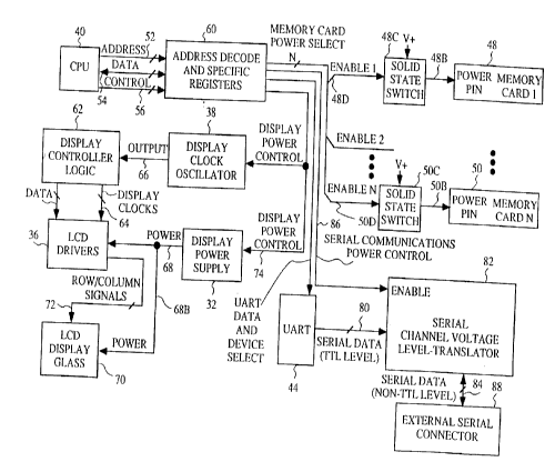
First, for the display, the power supply circuit 32
as shown in Figure 2 can be turned off. Also, the LCD driver
chips 36 which drive the actual display 70 can be disabled.
The clock oscillator 38 for the display can be disabled. The
software performs the above functions by controlling a bit in
particular register F6EC<bit 3>
CA 02282912 1999-09-24
23
accessible to the microprocessor 40 in the computer (see port
map, Table 3). Second, for the serial communications portion of
the computer, the power supply circuits (not shown) can~be
disabled by register F6EC<bit 5>. Also the oscillator (not
shown) which generates a timing signal for the UART 44 can be
disabled by register F6EC<bit 7> (see port map, Table 3). Third,
the clock for controlling CPU 40 can be turned off, as discussed
above, thereby not switching transistors which respond to the
software being executed if the software is in an idle loop.
An alternative embodiment includes at least one memory card
48, 50 which provides the nonvolatile memory. A power pin 48B,
50B of each memory card 48, 50 is controlled, allowing a computer
power supply (not shown) to provide power to memory chips (not
shown) which are internal to each memory card 48, 50. A fourth
portion of the computer comprising the memory cards may also be
powered up only as needed. Two memory cards 48, 50 are shown;
others may be provided. The power to each memory card 48, 50 is
turned off by a solid state switch 48C, 50C. The switches 48C,
50C, one of which is provided for each memory card 48, 50 are
controlled automatically based on an address decode, or are
controlled by a bit in a particular register accessible to the
microprocessor 40.
As shown in Fig. 2, the CPU 40 (i.e., the central processing
unit or processor, preferably a microprocessor), is connected to
address lines 52, data lines 54, and control lines 56 which carry
signals for decoding valid addresses. The microprocessor 40 is
connected by these lines 52, 54, 56 to the address decode logic
and specific registers circuitry 60. The circuitry 60 as shown
includes all the logic needed to decode addresses in the
CA 02282912 1999-09-24
24
microprocessor 40. Some addresses cause enable and select
signals during a microprocessor instruction processing cycle.
Other addresses correspond to specific ports accessible ~to the
microprocessor 40 (see port map, Tables 1, ~ and ~). when a
specific port address is decoded along with an instruction to
perform an input/output write, then the microprocessor data is
latched into a register, which is referred to as a specific
register. If the operation is a read operation, then this logic
circuitry 60 gates the appropriate data onto the microprocessor
bus, i.e., the data line 54 to the microprocessor 40.
Display Power Management
The display controller logic circuitry 62 includes all the
logic which allows the computer to emulate the conventional IBM
PC computer compatible display standards known as MDA and CGA
described in The New Peter Norton Programmer's Guide to the IBM
PC & PS/2. This circuitry 62 also generates the clock timing
signals 64 needed by the display LCD driver circuitry 36 from the
display clock signal 66 provided by the oscillator 38 for the
display clock. The oscillator 38 for the display clock is the
actual oscillator which generates the timing for the display
clock signal 64. The power control signal 68 for the display 70
enables the oscillator 38 for the display clock signals 64.
The LCD drivers 36 are the driver circuits which demultiplex
the data from the display controller logic circuitry 62 and
present the row and column data 72 to the LCD display glass 70.
The LCD display glass 70 is the actual LCD physical display which
the user of the computer views. The LCD drivers 36 are powered
by the display power supply 32. The display power supply 32 is a
CA 02282912 1999-09-24
switching power supply which generates all the necessary voltage
levels to drive the LCD display glass 70. The display power
supply 32 is controlled by a display power control signal 74
provided from the address decode logic and specific registers
5 circuitry 60. The display power control signal 74 thus turns off
the display power supply 32 when the display is not in use. The
LCD display glass 70 receives demultiplexed row and column data
72 from the LCD drivers 36, and obtains its power 68B from the
display power supply 32.
Communication Power Management
The UART 44 produces TTL (transistor-transistor logic)
voltage level signals 80 which are translated sows to conform to
conventional communications standards such as RS-232-C. The UART
44 also requires that incoming data be translated back to TTL
voltage levels. The serial channel voltage level translator
circuitry 82 accomplishes this function. The serial channel
voltage level translator 82 translates voltage levels between
those of one of the conventional communications standards 84 as
described above and TTL voltage levels 80. The non-TTL voltage
levels 80 are generated by the serial channel voltage level
translator circuitry 82 using switching techniques as is
conventional. The power supply of translator 82 will operate
only when enabled by the serial communications power control
signal 86, which is preferably under software control as a
specific register bit F6EC<7 bit> (see port map, Table 3).
The external serial connector 88 is a connector preferably
located externally to the case of the computer. This connector
88 connects serial devices to the computer. All signals 84 at
CA 02282912 1999-09-24
25a
this connector are non-TTL and require translation of voltage
levels before reaching
CA 02282912 2000-OS-18
70128-228D
- 26 -
the UART 44.
Memory Card Power Management
In one embodiment, a solid state switch 48C, 50C
controls the power pin 48B, 50B of each of the memory cards 48,
50 as described above. An enable signal 48D, 50D, derived from
decoding of memory addresses by the address decode and specific
register circuitry 60, or by a bit in a specific register (see
port map, Table 3) controls the solid state switches 48C, 50C.
The enable signal 48D, 50D turns power on to a memory card 48,
50 only when that particular memory card is to be accessed.
The above described circuitry is controlled by a
control program executed by the microprocessor 40, i.e., the
CPU. This control program is preferably an assembly language
microprocessor program. Further details of the operation of
this control program as it pertains to power management are
provided below. Hereinafter follows a brief description of the
operation of this control program.
With regard to the display power supply 32, the
control program detects either a user request to turn the
computer off (by means of an on/off switch) (not shown) or
detects inactivity (i.e., an idle state) of the computer over a
period of time. A particular bit is changed in a specific
register accessible to the microprocessor 40 turning off the
display related circuitry register F6EC<bit 3> (see port map,
Table 3). The control program detects either a user request to
turn the system on (by means of the ON/OFF switch) or a
programmed event which is to turn the system off.
With regard to the serial communications power supply
software, usage of the UART 44 is detected either by a service
request to the control program or by an interrupt, as described
below. A particular bit is changed in a specific register
F6EC<bit 5> accessible to the microprocessor 40 turning on the
circuitry related to
CA 02282912 1999-09-24
27
communications (see port map, Table 3). The termination of_
communications services by the user of the computer is detected
either by a request to the control program or by detecting a lack
of communications activity. A particular bit is changed in a
specific register F6EC<bit 7> accessible to the microprocessor 40
turning off the hardware circuitry relating to communications
(see port map, Table 3).
For the memory card power supply, memory card 48, 50 access
by the computer is detected either by a service request to the
control program or automatically through address decoding. If
the automatic mode is not in use, then a particular bit is
changed in a specific register accessible to the microprocessor
40 thus turning on power to the memory card 48, 50 for the
duration of the access to the memory card.
Flow charts for the power management related events are
shown here in Figures 3 and 4. Figure 3 shows hardware events
which cause the microprocessor clock to turn on or off and Figure
4 shows software events which cause the microprocessor clock to
turn off or prevent turning off the microprocessor clock.
Description of the Hardware Activity Circuitry
In the preferred embodiment of the invention, in order to
conserve power and extend the battery life of the computer, the
hardware of the computer, i.e., the circuitry, as described
above, is partitioned into sections based on the need for clock
signals. The oscillators which provide the clock signals to
different portions of the computer are enabled and disabled based
upon the demand for their services. Disabling an oscillator when
CA 02282912 2000-OS-18
70128-228D
- 28 -
it is not needed conserves power. In accordance with the
invention, those oscillators which are dormant, i.e., disabled
at a particular time, are started in a fashion so as to be
glitch free, that is to provide clock signals only when stable.
Since the oscillators take a period of time after being turned
on to stabilize, circuits are provided to start the oscillator,
then wait an appropriate amount of time before allowing the
oscillator signal to reach any of the logic circuitry which it
drives. For the oscillator which generates the timing signal
for the microprocessor clock, a voltage controlled oscillator
is provided having a frequency which is a function of the
system power supply output voltage. Thus since the power
supply voltage is under software control, the microprocessor
clock frequency is also under software control.
Detecting whether the computer is in an idle state is
important when determining if it is appropriate to stop the
clock signal to the microprocessor. The computer processor 40
is in an idle state when it is not acting upon user generated
input. In order for the control program in the microprocessor
to differentiate between an idle state and an active state, the
microprocessor control program must have knowledge of hardware
activity. Circuitry is provided in accordance with the
invention to monitor the computer circuitry (see Figure 2) and
alert the control program by way of an interrupt when
particular hardware events occur.
In one preferred embodiment of the invention, four
hardware events are monitored by the control program and appear
to the control program as nonmaskable interrupts (NMIs). These
four hardware events are the system timer tick, keyboard
activity, communications port activity, and on/off switch
activity.
Figure 3 shows a block diagram of hardware events
monitored by the power management control program of the
present invention.
CA 02282912 2000-OS-18
70128-228D
- 29 -
As in conventional MS-DOS compatible computers,
programmable interval timer 107 is provided for generating
timing signals for which the interval can be programmed.
According to the present invention, a second timer 98 is
provided for use by the power management system of the present
invention which can be programmed to generate a timer tick 100
at predetermined intervals. The timer tick 100 is used as a
time reference and a watchdog timer. The timer tick 100
provides periodic ticks 100 which are treated by the BIOS as
nonmaskable interrupts (NMIs) which are used by the BIOS (basic
input output system) control program in maintaining control of
the system despite badly behaved application programs, such as
word processing or spread sheets, running on the computer.
The presence of keyboard activity causes most
keystrokes to be stored in a buffer until acted upon by the
software. Typically the application program cycles
periodically through a loop which includes looking for keyboard
activity (looking for entries in the keyboard buffer). For
example, if an application program is loading a large file onto
disk or other mass storage memory, the program may also
periodically look for pressing of certain keys so that the user
has the opportunity to stop the operation of writing to memory
before the operation is complete. Such opportunities for the
user to interrupt the program while it is performing other
functions are commonly provided in application programs. At
other points in a program, there may be no other functions
happening except that the program is waiting for a keystroke.
Since the microprocessor speed is typically much
greater than the typing speed of the user of the computer, it
is desirable to conserve power by stopping (i.e., not clocking)
the microprocessor between keystrokes when the user is typing
and the program is performing no other function except
processing the response to the typing, which typically occurs
in a small part of the time between keystrokes. In this
CA 02282912 2000-OS-18
70128-228D
- 30 -
situation, the software is in an idle state, that is, the
microprocessor can be stopped without delaying the computer's
response to a user. In order for the computer to stop and
restart the microprocessor, the computer must include hardware
to restart the microprocessor in response to an external event.
The microprocessor goes into the compute mode as described
above, as a result of a keypress.
Note that in the preferred embodiment of the
invention the so-called power on/off switch 114 does not
actually turn power on and off but merely provides information
to the control system. Since the computer itself is always
powered, there is preferably no conventional power switch.
Instead the computer is provided with a switch which the user
uses to toggle between the off and on states. In the off state
the display is off, keystrokes are ignored, the processor is
stopped and timer ticks occur at long (i.e., about one minute)
intervals. However the computer itself is not truly off. An
NMI can be generated when the on/off switch is switched off so
that the control program will know that the user wishes to
toggle the computer from the off to the on state. Pressing the
on/off switch when the computer is switched off causes the
computer to move to the compute mode.
As shown in Figure 3 in block diagram form, the
circuitry of the preferred embodiment of the invention operates
as follows. A nonmaskable timer interrupt 100 (NMI) is
provided by a low frequency oscillator connected to timer 98
which is always running (as long as the batteries are
installed). The frequency of the low frequency oscillator is
divided down and can generate interrupts either every 54.9
milliseconds or approximately every minute. The choice of the
interrupt timing interval is programmable. An interrupt timing
interval shorter than 54.9 milliseconds allows faster cutoff of
the microprocessor clock in response to an idle state, with a
consequent saving of power. However, the interval should be
CA 02282912 2000-OS-18
70128-228D
- 31 -
long enough that multiple events indicating idle activity can
be observed within a single interval.
Two interrupts can be generated as a result of this
divided frequency. The first interrupt is designated IRQO, and
is compatible with the standard IBM PC timer interrupt which is
connected as the highest priority interrupt (IRQO) on an 8259-
compatible interrupt controller. As shown in Figure 3, a
standard IBM compatible programmable interval timer 107
generates this IRQO interrupt, which is sent to 8259 interrupt
controller 105, which in turn sends interrupt 103 to the
interrupt port of CPU 40. This interrupt is maskable and
compatible to that in the conventional IBM PC-XT computer and
is used by programmers to implement such functions as updating
the time-of-day clock and initiating any software activities
which are programmed to respond to the timer tick. The second
interrupt is a power management timer interrupt 100. Although
this interrupt 100 can be generated from the same timer 107 as
used to generate the IBM PC compatible interrupt IRQO, the
preferred embodiment uses a second power management timer 98 to
generate interrupt 100. This provision of a second timer
allows the timer interval of timer 98 to be varied by the
control program of the present invention while the interval of
IBM compatible timer 107 is varied by programmers of IBM and
DOS compatible computer programs.
This timer interrupt 100 is read by NMI interrupt
controller 101 as a nonmaskable interrupt. NMI interrupt
controller responds to interrupt 100 by sending a nonmaskable
interrupt 102 to the NMI port of CPU 40. This interrupt 102
takes priority over the 8259-compatible interrupt. This
interrupt 102 has an indicator bit in a particular register
F6E7<bit 6> accessible to the microprocessor 40 to allow
software to determine that a timer 100 interrupt was the cause
of the nonmaskable interrupt 102 (see port map, Table 3). The
CA 02282912 2000-OS-18
70128-228D
- 32 -
timer interrupt 100 can be programmed to automatically start
the clock (not shown) to the microprocessor 40.
Another type of interrupt is the keyboard interrupt.
When the keyboard circuits are enabled and scanning the
keyboard, a signal is generated by keyboard control circuitry
106 any time that a key is pressed, released, or pressed long
enough for an automatic repeat. Two interrupts are generated
when keyboard activity is detected. The first interrupt is
designated IRQ1. This is the conventional IBM PC-XT keyboard
interrupt which is connected in a conventional IBM PC-XT
computer as the second highest priority interrupt (IRQ1) on the
8259 interrupt controller. As shown in the embodiment of
Figure 3, the IRQ1 interrupt generated by keyboard control
circuitry 106 is provided to 8259-compatible interrupt
controller 105. This interrupt is maskable by the 8259-
compatible interrupt controller 105 in response to a masking
signal (not shown) equivalent to interrupt masks 110 and is IBM
PC-XT compatible. If enabled, interrupt IRQ1 causes interrupt
controller 105 to send an interrupt 103 to CPU 40.
The second interrupt is the keyboard NMI interrupt
104. It is necessary to provide a separate interrupt to
interrupt controller 101 which does not pass through CPU 40 so
that keyboard activity can be detected when CPU 40 is not being
clocked, so that the clock to CPU 40 can be turned on in
response to a key press. Further, certain keys are provided
for which the IRQ1 interrupt is not responded to. For example,
a key combination for controlling screen brightness generates a
keyboard interrupt 104 which causes NMI interrupt controller
102 to turn on CPU 40. But this particular key combination
when read by CPU 40 initiates other hardware activity for
controlling screen brightness and does not cause 8259
compatible interrupt controller 105 to generate an interrupt
103 to CPU 40. Interrupt controller 101 responds to a keyboard
NMI interrupt 104 by generating an NMI 102. This interrupt 102
CA 02282912 2000-OS-18
70128-228D
- 33 -
takes priority over the 8259 compatible interrupts 103 and
places an indicator bit in a particular register (F6E7<bit 7>)
accessible to microprocessor 40 to allow software to determine
that a keyboard interrupt 104 was the cause of the NMI (see
port map, Table 3). The keyboard interrupt 104 can be
programmed to automatically start the clock to the
microprocessor 40.
In the embodiment of Figure 3, power management can
also respond to activity on the communications port of the
computer.
UART controller 109
In response to activity on the communications port,
in addition to generating IBM compatible interrupt signal IRQ4,
which causes 8259-compatible interrupt controller 105 to
generate CPU 40 interrupt 103, UART controller 109 generates a
UART NMI 117, which causes NMI interrupt controller 101 to
generate NMI interrupt 102 which restarts the clock to CPU 40.
This ability to restart the CPU clock in response to UART
activity allows the CPU clock to be turned off between bytes of
information coming to or from the external port on the
computer.
The on/off switch 114 when pressed generates an NMI
116. An indicator 112 is provided in a particular register
F6EA<bit 0> accessible to the microprocessor 40 to indicate
that the on/off switch 114 was the cause of an NMI (see port
map, Table 3). An indicator 112 is also provided in a
particular register accessible to the microprocessor 40 to
indicate the current state of the on/off switch 114. The
on/off switch interrupt 116 can be programmed to automatically
start the processor 40 clock.
The above described circuitry operates with the
following software features. As shown in Figure 3, timer
interrupt 100 is presented to interrupt controller 101, and
CA 02282912 2000-OS-18
70128-228D
- 34 -
does not interfere with application programs which use the IRQO
interrupt. In another embodiment, not shown, the timer
interrupt is presented on the IRQO pin of the 8259-compatible
interrupt controller 101 and is IBM PC compatible. In this
case, timer interrupt 100 may be used for determining the time
of day as well as responding to other application program
commands. In the embodiment of Figure 3, the timer tick 100
interval is programmable to switch between the IBM PC-XT
compatible 54.9 millisecond time interval and a one minute
(approximately) time interval for power management and is not
accessed by application programs. When the computer is in the
off mode, the one minute interval is more desirable because it
causes less processor 40 activity and thus less power
consumption. The timer interrupt NMI 100 may be enabled by
changing a particular bit in a register (F6E9<bit 4>)
accessible to the microprocessor 40 (see port map, Table 3).
The timer interrupt 100 can be used by the control program to
maintain command of the system even if an application program
being executed revectors the timer interrupt IRQO.
With regard to the keyboard interrupt circuitry 106,
interrupts 104 presented on the IRQ1 pin of the 8259-compatible
Interrupt Controller 105 are IBM PC compatible and may be used
for keyboard services (responding to key presses). The
keyboard interrupt NMI 104 also can be used by the control
program to maintain command of the system even if a program
revectors the service routine for the 8259-compatible Interrupt
Controller 105. In order to conserve power, the microprocessor
40 clock may be stopped when it has been determined that a
program is waiting for keyboard input. When an NMI 104 is
generated as the result of keyboard activity, the processor 40
clock will restart again and the control program can allow
processing to continue.
With regard to the on/off switch 114, once a user has
finished using the computer for a period of time, the user can
CA 02282912 2000-OS-18
70128-228D
- 35 -
signal the control program that the user is finished by
activating the on/off switch 114. when a user wishes to use
the computer, he may activate the on/off switch 114 requesting
the control program to start up the computer and resume exactly
where he left off his previous usage. When the switch 114 is
activated, an NMI 116 is generated as described above. An NMI
routine is provided which will then determine that the on/off
switch 114 caused the interrupt by examining the appropriate
indicator 112 bit in a register F6EA<bit 0> accessible to the
microprocessor 40 (see port map, Table 3). The NMI routine
then debounces the switch by repeatedly examining the real time
status of the on/off switch 114 located in the particular
register accessible to the microprocessor 40 until the signal
is stable. Once the switch 114 has been debounced, the control
program can move the system between the off and compute modes.
With regard to Figure 3 as described above, the
microprocessor 40 address lines 54, data lines 52 and control
lines 56 are used to decode valid addresses for the circuitry
as shown. The address decode and specific registers 60 include
all the logic to decode the microprocessor addresses. Some
addresses are used as interrupt masks 110. Other addresses
correspond to status indicators 112 which the microprocessor 40
can read to determine the source of the interrupt. With regard
to the interrupt controller 101, only those interrupts
associated with power management are shown in Figure 3. The
interrupt controller 101 monitors all interrupt sources. If an
interrupt 100, 104, 116 or 117 takes place then an NMI 102 is
generated only if the interrupt 100, 104, 116 or 117 has been
enabled as indicated by interrupt masks 110. The NMI
interrupts 100, 104, 116, and 117 are enabled by changing the
appropriate bits in a specific register such as F6E8 and F6E9
accessible to the microprocessor 40 (see port map, Table 3).
If an interrupt 100, 104, 116 or 117 is enabled and does occur,
the source of the interrupt can be determined by examining the
CA 02282912 2000-OS-18
70128-228D
- 36 -
interrupt indicators 112 provided to the interrupt controller
101 through specific registers 60 accessible to the
microprocessor 40.
With regard to the timer 100, this is the above
mentioned system timer used for determining time of day and
watchdog timer functions. The interrupt controller 101 may be
programmed to cause an NMI 102 for each tick 100 of the timer
98. With regard to the keyboard control 106, the interrupt
controller 101 may be programmed to cause an NMI 102 with each
keypress, key release, or key repeat. With regard to UART
Control 109, the interrupt controller 101 may be programmed to
cause an NMI 102 with each receipt of a signal at the
communications port. With regard to the on/off switch 114, the
interrupt controller 101 is programmed to generate an NMI 102
any time this switch is activated.
Description of the Software Activity Detecting Circuitry
The above described interrupts provide several means
for returning the computer to the higher power compute mode
from one of its low power modes. The greater problem is when
to take the computer out of the higher power compute mode,
thereby extending battery life without inconveniencing the
user. The problem is to determine when an executing software
program is in a loop (in compute mode) looking for an external
event such as a keypress or a port signal and can be halted
without halting desired operations in progress. In order to
recognize unnecessary loop activities, it is necessary for the
power management system of the present invention to anticipate
how a software programmer will have written the code to place
the program into one of these loops, and determine when the
program can be safely halted without halting useful operations.
The badly behaved applications programs, which
include many of the commonly available commercial application
programs, often fulfill their input/output needs by direct
CA 02282912 2000-OS-18
70128-228D
- 37 -
hardware control rather than through the BIOS services. These
badly behaved programs can prevent control program intervention
and hence hinder system power management. In order to maintain
the desired control of the system in accordance with the
invention, the control program monitors various software
activities of the application programs.
For determining when the microprocessor clock can be
turned off during the execution of an application program,
particular circuitry is included in the computer in accordance
with the invention to detect the activity of software
application programs. When a particular sought for activity is
detected an NMI is generated if enabled.
As shown in Figure 4, there are two kinds of software
activities monitored by the power management system of the
present invention. UART clock control monitor 128 monitors a
software activity of waiting for a byte of information from the
communications port or waiting for the proper time to place a
byte of information on the communications port. Similarly,
INTTI6h trap 124 monitors a software activity of either waiting
for a key to be pressed or looking at the keyboard buffer to
see if a keypress is stored. This interrupt INTl6h is
conventionally used for keyboard services on IBM PC compatible
computers. Trapping a program using INTl6h will allow the BIOS
control program in the computer to maintain control of the
system and thus continue to conserve power by stopping the
processor clock between key presses.
Other software application program activities may be
interspersed with activities for which it is otherwise possible
to turn off the processor clock. When these activities are
occurring, the microprocessor clock should not be turned off
because the application program is not in an idle state and
turning off the clock would delay the computer's response to
the user. When these other activities are occurring, the
microprocessor clock is not turned off in response to the NMI
CA 02282912 2000-OS-18
70128-228D
- 38 -
126 generated by UART clock control interrupt 128 or the INTl6h
NMI interrupt 122 generated by an INTl6h trap 124.
Activities monitored by the novel BIOS control
program embodiment of Figure 4 are an I/O read/write
(communication with external devices such as a parallel
printer, external memory, or other devices not handled by the
DART) as monitored by I/O read/write monitor 132, DART activity
(successive bits in a single byte sent to an RS-232 port) as
monitored by UART activity monitor 134, waiting for a tick of
the programmable interval timer 107 as monitored by
programmable interval timer 136, writing to a screen, as
monitored by video access monitor 138, and writing to or
reading from disk, as monitored by mass storage monitor 111.
Mass storage monitor 111 is shown in both Figure 3 and Figure 4
because the single bit of data provided by mass storage monitor
111 indicates activity of both hardware and software.
Additional instructions which are not shown in Figure 4, but
can also be monitored include CPU opcodes (for example,
multiply).
As provided by the control program, the CPU places on
the address bus 54 and control lines 56 the address of these
registers 132, 134, 136, 138, and 111. Data are in return
provided on data lines 52 indicating to CPU 40 the status of
the activity being examined.
When any of these activities are being performed by
the application programs, related bits are set in address
decode and specific registers 60 through data line 52b, and
prevent the turning off of the CPU 40 clock. By detecting
activities requiring the microprocessor clock to be running
interspersed with other activities which if alone would not
inconvenience the user if the clock were off, it is possible to
use lower criteria for repeated activity of the INTl6h trap and
UART clock control in determining when to turn off the clock.
CA 02282912 2000-OS-18
70128-228D
- 39 -
The reason the programmable interval timer activity
becomes a reason not to turn off the clock in spite of
apparently idle activity, is that programmers use this
programmable interval to control the speed of other events, for
example movement of objects across the screen in a game
program, and turning off the computer would interfere with the
rhythm of the program. Further, when the program was turned
back on, the loop would be entered again, such that programs
using the programmable interval timer could not be operated
under the power management system of the present invention.
The following describes the circuitry 124 and 128
which looks for the INTl6h and UART software activities.
First, regarding the INTl6h trap 124, a software INTl6h
instructions causes the microprocessor 40 to read four bytes
from the computer memory (now shown) starting at the address
58h bytes from the beginning of the interrupt vector table.
The INTl6h interrupt 122 is intended to trap a software event
that is the execution of the INTl6h instruction. Since each
interrupt vector occupies four bytes in the interrupt vector
table, circuitry 124 is provided to monitor the first byte of
the table entry for INTl6h, which is located 58h bytes from the
beginning of the interrupt vector table in low memory. Any
read of data by CPU 40 from this memory address can cause an
NMI 122. If an interrupt 122 is generated, an indicator bit in
a particular register (F6E4<bit 7>) accessible to the
microprocessor 40 is set (see port map, Table 3).
The novel software associated with trapping typical
software events functions as follows. With regard to the
INTl6h interrupt 122, the goal, as described above, is to trap
a software program which has issued the INTl6h instruction.
Since this interrupt 122 is typically used for keyboard
servicing, intercepting an INTl6h instruction allows the
control program to detect an applications program looking for
keystrokes. If the novel control program of the present
CA 02282912 2000-OS-18
70128-228D
- 39a -
invention obtains an NMI 122 caused by INTl6h, the control
program examines the argument (i.e., a particular INTl6h
service) passed to the INTl6h interrupt handler and indicates
what the calling applications program was trying to accomplish.
CA 02282912 1999-09-24
The simplest function for which power saving can be
initiated is the call to wait for a key to be pressed. If the
calling applications program wanted to wait for a key to be
pressed, then the microprocessor can be stopped immediately until
5 a key is pressed. However, if the applications program is
periodically checking the keyboard buffer with an INTl6h call to
see if a key has been pressed, then a guess may be made based on,
for instance, statistics (i.e., how many times the INTl6h
interrupt 122 was invoked per time period) to decide if and when
10 the processor 40 clock should be stopped.
Since the display controller logic is designed to conserve
power also, certain control program intervention may be required
when software application programs access the video display of
the computer. Some application programs allow for a user to
15 interrupt the application program while the application program
is in the midst of writing on the screen. These application
programs will insert INTl6h calls into other screen writing
activities. Such INTl6h calls should not be used to turn off the
microprocessor. Means for distinguishing INTl6h calls during
20 screen writes from INTl6h calls in other loop activities waiting
for outside input are discussed later. However, as discussed
above under display power management, the present invention
allows for the microprocessor clock to be turned off while the
screen is being refreshed but its contents are not being changed.
25 The screen refresh is not handled by the microprocessor and can
proceed normally even though the microprocessor is turned off.
Thus, the display controller controls two functions, generating
characters to be displayed on the
CA 02282912 2000-OS-18
70128-228D
- 41 -
screen which requires the microprocessor to be on, and
refreshing a static screen which does not require the
microprocessor to be on. A bit is set to alert the control
program of the display controller status, in particular when
the display controller is performing a screen write which
requires the microprocessor to be on.
Applications programs which use the UART directly
without the aid of BIOS would find the communications system
unstable or unusable when used with the power management system
of the present invention if no provision were made for
stabilizing the lock oscillator before connecting the clock.
In order to assist such applications programs, an NMI is
enabled to cause a delay loop when a write or read from the
DART occurs. With regard to the UART interrupt 126 shown in
Figure 4, any read or write to an address specific to the UART
128 will cause an NMI 126 if enabled by changing an appropriate
bit in a particular register accessible to the microprocessor
40. This information is used by the control program to monitor
the start-up of the UART clock oscillator to ensure that the
UART baud clock oscillator (not shown) is stable before a
program is allowed to proceed with further UART activity. This
information is also used by the control program to know when
another applications program is utilizing the UART through
direct hardware control techniques. This is not possible on a
typical prior art IBM PC-XT compatible computer.
Power Management Software
The conventional ROM BIOS functionality available in
prior art computers is extended in accordance with the present
invention by means of additional software functions and
services, which are accessed by any application program through
a conventional interface of software interrupts as used by ROM
BIOS and MS-DOS. The IBM PC-XT compatible ROM BIOS function
designated "get keypress" operates nonconventionally in
CA 02282912 2000-OS-18
70128-228D
- 42 -
accordance with the invention to power off as much of the
computer system as possible at any one time, instead of sitting
in an idle loop as is done in the prior art computers. This
function is linked to circuitry so that the enhanced software
is invoked when a keypress is detected. The conventional IBM
PC compatible ROM BIOS funtion "get keyboard status" is
modified so that a count of the number of times a call is made
to this function over a given time period is monitored. After
a certain time, it is safe to assume that the application
program is idle, that is, waiting for user input. If the
conditions of the algorithm are satisfied then it is safe to
stop the microprocessor until a key is pressed. The
microprocessor may be stopped whenever there has been no
keyboard or significant microprocessor computing activity for a
given time, i.e., preferably approximately 100 milliseconds.
The algorithm for determining when the microprocessor
can safely be shut off according to the above requirement for a
given time is to count the number of times an INTl6h call has
been made during an interval between timer ticks, and shut off
the microprocessor when the number exceeds a specified value.
However, it is not preferred to check for an
application program being haltable simply by counting the
number of times the program has used INTl6h to check the
keyboard buffer since the last keypress. An absolute number of
checks has been shown with a variety of application programs
either to cause the computer to turn off the program when other
significant computation is going on (a condition unacceptable
to the user) in the case when the number of checks between
timer ticks has been set too low, or to cause the computer to
remain on when the program is in a loop (a condition which
shortens battery life). Application programs have been
observed to send INTl6h commands as few as seven times per
timer tick and as many as 250 times per timer tick, both
extremes occurring in programs which were in a repetitive loop
CA 02282912 2000-OS-18
70128-228D
- 43 -
during which the microprocessor could be turned off. However,
programs which are performing other useful operations such as
writing to memory have been observed to make as many as 10
INTl6h calls per timer tick, and would be erroneously shut off
by an algorithm which used the criterion of requiring only
seven INTl6h calls per timer tick.
Figs. 6A through 6G show results of these application
program observations. Fig. 6A shows a graph of many
observations of a Lotus 123 program's use of INTl6h calls when
the processor is operating at a 1.3 MHz rate and timer ticks
are occurring every 54.9 milliseconds. Fig. 6A accumulates
observations of the Lotus 123 program's behavior over
approximately a 1-minute period. During the first
approximately 15 seconds after the observations begin, the
program is performing a calculation during which it looks for
key presses with INTl6h calls only twice during one of the
timer tick period. Between 15 seconds and 19 seconds, the
program looks for key presses about 7 or 8 times between timer
ticks. At about 19 seconds, the program ceases looking for key
presses for a short time while other computations are performed
in response to a key press. Such activity occurs again at
approximately 23 seconds. At approximately 24 seconds a
lengthier calculation prevents INTl6h calls for key presses.
Thus the microprocessor could have been off for most of the
time between 15 and 23 seconds. An algorithm for saving power
must recognize this possibility. It is clear from the general
shape of the graph of Fig. 6A that the frequency of INTl6h
calls has only a few values, predominantly zero and 7 or 8.
(The value 7 or 8 probably represents the same loop and the
difference of one simply represents round-off error).
As shown in Fig. 6B, the same Lotus 123 program
running at a 7 MHz clock speed repeats its loop more frequently
between timer ticks of 54.9 milliseconds. Thus, the INTl6h
calls almost always occur approximately 40 times per timer tick
CA 02282912 2000-OS-18
70128-228D
- 44 -
when they occur at all, the vertical white lines indicating
zero times per timer tick when active computing is being done.
The portion of the graph under the curve represents time when
unnecessary power is being consumed needlessly running the
microprocessor, and for which an algorithm is desired for
turning off the microprocessor.
A more sophisticated algorithm improves the power
management ability of the present invention. One such
algorithm which allows hardware to detect most loop activity
which could be eliminated by turning off the microprocessor and
which does not cause the microprocessor to be turned off when
useful computation is occurring is to compare the number of
INTl6h calls during one timer tick interval to the number of
INTl6h calls during the previous timer tick interval. If these
numbers are the same (or differ by only one count), it is
likely that the computer is in a loop and that the
microprocessor can be turned off. Finding two time periods
with the same number of INTl6h calls in which the number is
greater than a minimum value of about 4 is an algorithm for
turning off the microprocessor which is much preferred over
providing an absolute count which must be exceeded during a
timer tick interval. Another algorithm which gives more
assurance that the microprocessor will not be erroneously
turned off, and which uses only a small amount of additional
power, involves requiring a string of three intervals during
which the number of INTl6h calls differs by no more than one.
The computer, however, need not be fully turned off.
In the case of an application program waiting for a keypress,
all sections of the computer are turned off with the exception
of the video display. The computer is then in display mode and
appears to the user to be continuously on, as keys are
periodically pressed, or communications are sent and received.
If there continues to be no activity for a longer given time,
CA 02282912 2000-OS-18
70128-228D
- 45 -
i.e., preferably approximately four minutes, then the video
display is turned off and the computer is in the off mode.
In accordance with the invention, the problem of
coping with badly behaved applications programs is solved by
providing hardware circuitry to notify the control program
software if an application is taking over control of the ROM
BIOS keyboard services. This method is accomplished by having
the hardware monitor a particular fixed memory location as
defined by the conventional IBM PC-XT specification used for
the software interrupt to access keyboard services, and
alerting the ROM BIOS if this occurs.
Figure 5 Flow Chart for Power Management
The power management control program in accordance
with the invention is illustrated in flow chart form in Figure
5. As shown in Figure 5, at the top of the flow chart the
system is in the compute mode 10. The computer can be put into
compute mode by a variety of events. The novel control program
first monitors the computer circuitry to determine what caused
a nonmaskable interrupt 102 (NMI) to place the computer into
compute mode 10. This part of the control program is referred
to as the NMI dispatcher 134. In the case of the power
management portion of the control program, there are five
activities which the NMI dispatcher 134 is looking for.
These five activities are, in the preferred
embodiment of the invention, software interrupt 122 (i.e.,
INTl6h) from trap 124 (see Figure 4), timer tick interrupts 100
(see Figure 3), interrupt 116 from the activation of the on/off
switch 114 (see also Figure 3) keyboard interrupts 104 (INT9)
(also see Figure 3) and screen write interrupt 176 (i.e.,
INT10). The on/off switch 114 is described above. The timer
tick interrupt 100 as described above is provided every 54.9
milliseconds (i.e., 18.2 times a second) and is programmably
CA 02282912 2000-OS-18
70128-228D
- 46 -
switchable as described above to approximately 1 tick per
minute.
Keyboard interrupts 104 are generated by the keyboard
control circuits 106 of Figure 3 each time a key is pressed,
released, or held long enough for it to repeat. In accordance
with a preferred embodiment of the invention, the keyboard
control circuits 106 (which in conventional systems are
provided by a separate device) are provided in an ASIC in the
computer. Preferably both the scanning and decoding of the
keyboard signals are performed in this ASIC.
Response to interrupt INTl6h trap 122 operates as
follows: after receipt of interrupt INTl6h trap 122, the
control program determines what function the software program
was trying to accomplish when it issued the INTl6h instruction.
Two possible functions are first, waiting for a keypress 140
and second of all, obtaining keyboard status 142. In the case
of waiting for a keypress 140 the system can immediately go to
display mode 16, in which the display is on and the other
hardware elements of the computer are off. This is what
happens when the computer is not computing and typically
waiting for the user of the computer to type. In the case when
INTl6h is used to obtain keyboard status 142, the control
program increments a counter 144. This counter 144 counts the
number of times the keyboard status 142 was checked using the
INTl6h instruction since the last timer tick 100. The point is
that if the application program is in a low intensity
processing mode or a zero intensity processing mode, the
keyboard status 142 will be checked many times. Thus within a
short time period there will be many counts accumulated in the
counter 144. This usually indicates that no significant amount
of processing is going on. As mentioned earlier, however, it
is preferable to compare the number of counts since the last
timer tick 100 to the number of counts in the previous
interval, since different software programs have widely
CA 02282912 2000-OS-18
70128-228D
- 47 -
different rates of using the INTl6h interrupt to check keyboard
status. Thus after updating the counter at step 144, the
control program returns the computer to compute mode 10 in
which the application program proceeds with its next
instruction. It is possible that many NMI 102 interrupts will
turn out to be INTl6h interrupts 122, that they will be status
requests 142, and that the counter will again be updated,
returning the computer to compute mode. After some period of
time, however, an NMI 102 interrupt will be found by NMI
dispatcher 134 to have been caused by a timer interrupt from a
timer tick 100. This timer interrupt 100 causes the computer
to enter a part of the program for determining whether it is
safe to turn off the microprocessor and halt the program being
executed without interfering with functions the user wants to
perform.
The following describes the operation of the control
program with regard to the timer tick interrupt 100. After the
NMI dispatcher 134 determines that the interrupt is a timer
interrupt 100, the control program at 148 determines whether
the computer is in the display (low power) mode 16 or off mode
12. At this point, if the computer is in the display mode 16,
the control program at 150 determines if the computer has been
in the display mode 16 for a predetermined period of time such
as greater than two to four minutes. If the control program
determines the computer was in off mode 12, it returns the
computer to off mode 12. If the system is in the display mode
16, but at 150 has been in that mode for less than a time of
approximately four minutes, then the system remains in the
display mode 16. If the computer has been in the display mode
16 for a period of greater than four minutes, which means that
a keypress or other activity which moves the computer into
compute mode 10 has not occurred for four minutes, the control
program puts the system into the off mode 12. The off mode 12
described above with regard to Figure 1 is a state in which the
CA 02282912 2000-OS-18
70128-228D
- 48 -
display is off, the microprocessor is off, the other sections
of the computer are off, and the timer is slowed down to
approximately 1 timer tick per minute. In off mode, the timer
interrupts 100 (see Figure 3) cycle the control program of
Figure 5 through the compute mode 10 and back to the off mode
about once per minute.
If the timer interrupt 100 causes the control program
to determine at step 148 that the computer is not in a low
power mode (thus it is in compute mode, communication mode, or
DMA mode as shown in Figure 1), then at step 154, the INTl6h
counter is examined to determine if the number of INTl6h
interrupts since the last timer interrupt 100 is greater than a
minimum number. A presently preferred minimum number is five.
If this minimum number such as five is exceeded, the control
program makes a comparison at step 184 between the number of
INTl6h interrupts in the last timer tick interval just
completed and the number of INTl6h interrupts in the previous
interval. Alternatively, the control program may compare the
number of INTl6h interrupts in three succeeding intervals. A
counter stores the number of INTl6h counts in several
successive timer tick intervals and the control program
continues to make this comparison once for every timer
interrupt 100.
If at step 184 the control program determines that
the number of INTl6h interrupts in the INTl6h counter differs
from the number in the previous interval, indicating that some
less repetitive activity is occurring, even if the number of
INTl6h interrupts is greater than the minimum number (such as
five), the control program will not turn off the microprocessor
clock and stop the executing application program, but will move
to step 181.
Regarding step 181, a power saving device described
more completely in copending application Serial No. 07/374,514,
attorney docket no. M-962, incorporated herein by reference,
CA 02282912 2000-OS-18
70128-228D
- 49 -
switches the system power supply voltage from a low voltage in
the range of 2 to 3 volts to 5 volts only when the computing
requirement are intense. The higher voltage causes the voltage
controlled oscillator which drives the microprocessor clock to
run at a faster speed, in the present case to speed up from
about 2 MHz to about 7 MHz. When the faster computing speed is
not needed, the computer operates at lower power and lower
speed, thereby saving considerable power. When the computer
first enters compute mode 10, the voltage is at the lower
level. Step 181, which is reached every time a power
management timer interrupt 100 occurs determines whether the
computer has been in compute mode more than R seconds,
presently preferred to be 1.5 seconds. If the computer has
been in compute mode 10 less than 1.5 seconds, the program
returns control to the application program in compute mode 10
and the system power supply remains at the low voltage. If the
computer has been in compute mode more than 1.5 seconds, the
control program at step 183 activates circuitry which increases
the voltage of the system power supply to 5 volts. This in
turn causes the voltage controlled oscillator which drives the
microprocessor clock to speed up, giving the user quicker
response to heavier computing requirements.
If the number of INTl6h interrupts in two or three
successive intervals differs by not more than a count of one
(for round-off error), then at step 184 the tolerance is
determined to be OK (the activity is determined to be
repetitive) .
There are application programs which use an INTl6h
call fairly frequently intermixed with other computations which
should not be halted. Some of these uses will produce INTl6h
calls in such a regular pattern that the above algorithm for
comparing INTl6h calls during two or three successive timer
tick intervals will find identical numbers of calls and would
erroneously turn off the microprocessor in the midst of an
CA 02282912 2000-OS-18
70128-228D
- 50 -
operation if no other tests were made. Examples of these
activities are writing to the screen, writing to mass storage
memory, and sending or receiving from a communications port.
In order to avoid erroneously turning off the computer during a
computation, the control program checks for these activities.
Variations of the control program check for different specific
activities. The control program shown in Fig. 5, after
determining at step 184 that two or three successive intervals
have the same number of INTl6h calls, checks at step 186 to see
if a screen write command (a video access command) has been
given since the last occurrence of timer interrupt 100. A
variation on the block diagram of Figure 5, discussed in
connection with Fig. 4, includes additional tests for disk or
other memory access and communications port access, with the
answer to each question being "no" before the program moves to
the low power display mode 16, in which the microprocessor
clock is off and the executing computer program is halted. A
further variation provides for forming a table of frequency of
INTl6h calls made by different programs and turning off when
the number of INTl6h calls matches the value in the table.
Similarly, at the beginning of an application program, the
control program can begin to form a history of INTl6h call
frequency and start responding to a particular frequency of
INTl6h calls when the history indicates the current frequency
is equal to the stable value. When the microprocessor clock is
off, the transistors necessary for moving quantities into and
out of memory and other such hardware operations necessary to
respond to software commands are halted, and use of power is
markedly reduced.
If the control program determines at step 186 that
the application program is writing to screen (video access), or
in another variation writing to mass memory, reading from mass
memory, writing to the communications port or reading from the
communications port (or other tests which may be preferred in a
CA 02282912 2000-OS-18
70128-228D
- 51 -
particular embodiment), the control program returns to compute
mode 10, and the application program takes over again.
Interrupt 116 is generated by the on/off switch 114
(see Figure 3) as described above. When the user activates the
on/off switch, then an NMI 116 is generated. The activation of
the on/off switch means, as determined at 156, either that the
computer is on and is being turned off or that the computer is
off and is being turned on. Thus as shown at step 156 if the
computer status is that it is on, activating the switch puts
the computer into the off mode 12. If the computer is off at
156 then activating the on/off switch causes the timer tick
circuit to be reprogrammed at 158 to provide timer ticks every
54.9 milliseconds. (As stated above, other intervals may be
selected.) The memory locations associated with keeping time
of day information are updated to reflect the transition to
timer ticks every 54.9 milliseconds instead of once per minute,
then the computer is returned to the compute mode 10. Updating
of the time of day information is performed by reading a
counter which counts and accumulates the number of 54.9
millisecond time periods which have passed since the counter
was last cleared. This counter preferably clears itself once
per 1024 time periods (56.2 seconds).
The next interrupt relevant to the power management
system is the keyboard interrupt 104, preferably INT9. As
described above interrupt 104 is generated by the keyboard
control circuitry 106 (see Figure 3) when a key is pressed or
released. Upon generation of a keyboard interrupt 104 the
above described INTl6h counter 144 is reset at step 160. After
this the key input is processed at 162 by the computer and
control is returned to the application program in compute mode
10. As shown by the dotted lines 164, 166, both the off mode
12 and the display mode 16 return control to the NMI dispatcher
134 periodically as determined by the system timer tick
interrupt 100.
CA 02282912 2000-OS-18
70128-228D
- 52 -
The last interrupt relevant to the power management
system embodiment of Figure 5 is screen write INT10 interrupt
176. INT10 is a standard BIOS call to cause a screen write.
The INT10 interrupt causes the BIOS to access the screen, as
was done by the video access call tested by hardware in block
186 discussed earlier. Another embodiment, not preferred,
responds to the INT10 call but does not detect at 186 a direct
video access. Indeed, if direct video access is detected at
186, detecting the INT10 call is not necessary, but is
preferred to give faster response before waiting for timer
interrupt 100.
Finally, manual means are also provided for putting
the computer into computer mode 10. There are programs which
will likely be erroneously shut off by the power management
system of the present invention if the embodiment selected has
parameters which produce significant power savings. In order
to allow such programs to run successfully, the computer
preferably includes means, for example a combination of
keystrokes, for disabling the power management feature of the
present invention. This disabling means is preferably used
only when the user has encountered a problem with the power
management system. In one embodiment a key press or key
combination causes power management to be overridden.
Overriding is accomplished in this embodiment by disabling the
timer interrupt 100 generated by timer 98.
In accordance with the invention, the control program
as described above is preferably written in assembly language
and is installed in ROM associated with the computer
microprocessor. This preferred assembly language is that which
is conventionally used for the Intel 8086 family of
microprocessors.
CA 02282912 2000-OS-18
70128-228D
- 53 -
The above description of the invention is
illustrative and not limiting. Other embodiments of the
invention will be apparent to one of ordinary skill in the art
in the light of the invention. The invention is not limited to
IBM PC XT compatible computers or to IBM PC compatible
computers. Also, the particular hardware and software
embodiment of the invention as described above are not intended
to be limiting, but illustrative. In other embodiments of the
invention more or less of the functions are provided in
hardware and/or software.