Note: Descriptions are shown in the official language in which they were submitted.
CA 02289984 1999-11-09
WO 98/53535 PCT/US98/08433
1
BEMICONDUCTOR MICRO-RESONATOR DEVICE
CROSS-REFERENCE TO RELATED APPLICATIONS
This is a continuation-in-part of United States
Patent Application 08/653,585 filed May 24, 1996 which is
a continuation-in-part of 08/450,284 filed May 25, 1995.
TECHNICAL FIELD
The present invention relates to an optical,
semiconductor micro-resonator device and more particularly
to such a device including a semiconductor microcavity
resonator, a first waveguide and a second waveguide.
Light props-gating in the first waveguide with a
wavelength off resonance with the microcavity resonator is
output from the first waveguide; whereas light propagating
in the first waveguide with a wavelength on resonance with
the microcavity resonator is coupled thereto and from the
microcavity resonator the light is coupled to the second
waveguide for output therefrom.
STATEMENT REGARDING FEDERAhLY
SPONSORED RESEARCH OR DEVELOPMENT
This work was supported by ARPA under contract
F49620-96-1-0262 and NSF Faculty Early Career Development
Award ECS-9502475.
BACKGROUND OF THE INVENTION
One known optical resonator as described in the
article "New Integrated Ring Resonator In Glass," W. J.
Wang et al., Elec. Lett., Vol. 28, no. 21, page 1967-1968,
October 8, 1992, is a large ring resonator formed of glass
that is used as a tunable wavelength selective filter for
various optical frequencies. The path length of the glass
resonator is on the order of 12 cm and it has a low
finesse of 5. This glass ring resonator is not suitable
for on-chip integration with semiconductor devices.
SUBSTITUTE SHEET (RULE 26)
CA 02289984 1999-11-09
WO 98/53535 PCT/US98108433
2
Another known resonator of smaller size and larger
finesse is described in the article "An Optical FDM
Distribution Experiment Using A High Finesse Waveguide-
Type Double Ring Resonator," K. Oda et al. IEEE Photonics
Tech. Lett., Vol. 6, no. 8, page 1031-1034, August 1994.
The frequency division multiplexing distribution scheme of
this article uses a Ge02-doped silica double ring resonator
having a diameter of 3500~m and a finesse of 200.
Although the diameter of the double ring resonator is
small compared to that of the glass resonator, the high
bending loss in the second ring of this resonator prevents
reduction in its size. Also, the second ring required to
attain the relatively high free spectral range (FSR) of
the device complicates the manufacturing process.
SUBS ~"~ i UTE SHEET (RULE 26)
CA 02289984 1999-11-09
WO 98/53535 PCT/US98108433
3
BRIEF SUN~IARY OF THE INVENTION
In accordance with the present invention, the
disadvantages of prior optical resonator devices have been
overcome. The optical resonator of the present invention
is a semiconductor micro-resonator device that is much
smaller in size than prior optical resonators. Because of
the small size, the quality factor Q of the cavity and the
finesse F of the device are potentially much higher than
prior resonators. In addition, the frequency spacing
between adjacent resonances of the cavity, referred to as
the free spectral range, is also larger. Further because
the resonator device of the present invention is
fabricated from semiconductor materials it is suitable for
on-chip integration with other semiconductor devices such
as a semiconductor laser. In particular, the possibility
of having resonator sizes of a few micrometers to tens of
micrometers in accordance with the present invention,
instead of resonator sizes on the order of hundreds or
thousands of micrometers as of prior devices, enables the
realization of ultra-high density photoriic integrated
circuits with component densities ten to ten thousand
times higher than is currently possible with known
devices.
More particularly, the micro-resonator device of the
present invention includes a microcavity resonator formed
of semiconductor materials and having a diameter of
approximately 56000~,1g/nres or less where the device is
designed for and has an associated operating range of
wavelengths of light; ~.lg is the longest operating
wavelength of light in units of Vim; and nrefi is the
effective propagating refractive index of light in the
microcavity resonator. The device also includes a first
waveguide formed of semiconductor materials with a portion
of the first waveguide disposed adjacent to the
microcavity resonator. A portion of a second waveguide
formed of semiconductor materials is also disposed
SUBSTITUTE SHEET (RULE 26)
CA 02289984 1999-11-09
WO 98/53535 PCT/US98/08433
4
adjacent to the microcavity resonator. Light propagating
in the first waveguide with a wavelength on resonance with
the microcavity resonator is coupled to the microcavity
resonator and from the microcavity resonator the light is
coupled to the second waveguide for output therefrom.
Light propagating in the first waveguide with a wavelength
that is off resonance with the microcavity resonator is
not coupled to the microcavity resonator but continues to
propagate in the first waveguide for output therefrom.
Unlike a Fabry-Perot type resonator, such as those formed
by two parallel mirrors or two sets of reflective
gratings, there is no feedback of the off resonance light
in the micro-resonator of the present invention.
The semiconductor micro-resonator device of the
present invention can either be a weakly-guiding device or
a strongly-guiding device. When formed as a weakly
guiding device, the diameter of the microcavity resonator
is in the range of 560~,1g/nreSN~m to 56000~.1g/nresN~m~ When
formed as a strongly-guiding device, the microcavity
resonator has a diameter as small as ~.lg/nres microns
through 560~,1g/n=es~.m~
The semiconductor micro-resonator device may be
employed as an electro-optical modulator, a switch, an
intensity modulator, a tunable optical filter, a phase
modulator, a wavelength-division multiplexor and
demultiplexor, among other applications. The high F of
the present invention is particularly advantageous for a
number of these applications since the resonator
potentially requires only a n/F phase shift instead of a n
phase shift within the cavity length, thereby reducing the
switching voltage by a factor of F. Further, the high
finesse and high free spectral range of the micro-
resonator device of the present invention allows high
wavelength resolution for demultiplexing applications and
also allows dense wavelength-division multiplexing schemes
which is particularly important when the device is to be
SUBSTITUTE SHEET (RULE 26)
CA 02289984 1999-11-09
WO 98153535 PCT/I3S98/08433
used in a communication network or the like.
These and other advantages and novel features of the
present invention, as well as details of an illustrated
embodiment thereof, will be more fully understood from the
5 following description and drawings.
SUBSTITUTE SHEET (RULE 26)
CA 02289984 1999-11-09
WO 98/53535 PCT/US98/08433
6
BRIEF DESCRIPTION OF THE SEVERAL
VIEWS OF THE DRAWINGS
Fig. lA is a diagram illustrating the geometry of the
semiconductor micro-resonator device of the present
invention having a microcavity resonator and adjacent
waveguides;
Fig. 1B is a cross sectional view of the
semiconductor materials forming the microcavity resonator
and the waveguides of Fig. lA;
Fig. 2A is an illustration of an image taken with an
infrared vidicon camera of the output from a port Z of a
first waveguide of Fig. lA;
Fig. 2B is an illustration of an image taken with an
infrared vidicon camera of the outputs from the respective
ports Y and Z of the respective second waveguide and the
first waveguide of Fig. lA as the light input to the first
waveguide is becoming on resonance with the micro
resonator disk;
Fig. 2C is an image taken with an infrared vidicon
camera of the outputs from the respective ports Y and Z of
the second and first waveguides when the wavelength of
light input to the first waveguide is tuned to on
resonance with the microcavity resonator disk;
Figs. 3A-D are graphs illustrating the reflectivity
of a respective 10~m microcavity disk, a 10~m microcavity
ring, a 20~m microcavity disk and a 20~m microcavity ring;
Figs. 4A-B respectively show graphs of the
unnormalized tranmissivity measured from the output port
of the second waveguide with a 10.5~m microcavity disk and
the full width half maximum d1.~", at the transmission peak;
Fig. 5 illustrates a second embodiment of the
semiconductor micro-resonator device of the present
invention wherein the waveguides are partially curved
about respective portions of the microcavity resonator
formed of a ring or a disk;
Fig. 6 is an illustration of an example of the
SUBSTITUTE SHEET (RULE 26)
CA 02289984 1999-11-09
WO 98/53535 PCT/US98/08433
7
semiconductor wafer layers forming the microcavity
resonator and waveguides in a weakly guiding device in
accordance with the present invention;
Fig. 7 is an illustration of another example of the
semiconductor wafer layers forming the microcavity
resonator and waveguides in a strongly guiding device in
accordance with the present invention;
Fig. 8 is a diagram illustrating the phase mismatch
between the first waveguide and the microcavity resonator
for a particular arc angle;
Fig. 9 illustrates one embodiment of a wavelength
demultiplexing scheme using the microcavity resonator of
the present invention;
Fig. 10 illustrates an embodiment of an electrically
tunable optical filter useable in a number of diverse
applications;
Figs. 11A and B are diagrams illustrating the
geometry of a respective disk and ring closed loop
microcavity resonator having an arbitrarily curved
circumference;
Figs. 12A-C illustrate the etching of various layers
of the wafer to form the microcavity resonator and
waveguides of a weakly guiding device;
Figs. 13A-C illustrate the etching of various layers
of the wafer to form the microcavity resonator and
waveguides of a strongly guiding device; and
Fig. 14 illustrates an embodiment of the present
invention with multiple output waveguides.
SUBSTITUTE SHEET (RULE 26)
CA 02289984 1999-11-09
WO 98/53535 PCT/US98/08433
8
DETAILED DESCRIPTION OF THE INVENTION
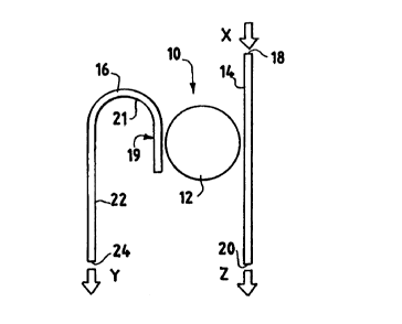
An optical, semiconductor micro-resonator device 10
as shown in Fig. lA includes a microcavity resonator 12
and a pair of waveguides 14 and 16. The microcavity
resonator has a range of operating wavelengths of light
and has a diameter of approximately 56000~,1g/nres or less
where ~,lg is the longest operating wavelength of light in
~m and nres is the effective propagating refractive index
of light in the resonator. For example, for ~.lg 1.5~m, the
diameter of the microcavity resonator can be 28000~m or
less. The microcavity resonator is formed as a closed-
loop resonator such as a disk or a ring. However, the
closed loop resonator may also have an arbitrarily curved
circumference in the form of a distorted disk or ring as
shown respectively in Figs. 11A and B. In the case of a
distorted disk or ring, the effective diameter of the
microcavity resonator is the diameter of the smallest
circle within which the entire area of the resonator 12
can be contained. It is also noted that the width of the
ring cavity need not be uniform but may vary throughout
the ring.
The waveguide 14 has an input port 18 labeled X and
an output port 20, labeled Z. The waveguide 16 has an
output port 24 labeled Y. A portion of the waveguide 14
as shown in Fig. 1 is adjacent and tangential, i.e. in the
direction of a tangent, to the microcavity resonator 12.
Similarly, a portion of the waveguide 16 is adjacent and
tangential to the micro-resonator 12. It is noted that
the respective portions of each of the waveguides 14 and
16 adjacent to the microcavity resonator 12 need not be
tangential but may curve around a portion of the
microcavity resonator 12 as described below with reference
to Fig. 8. Further, the microcavity resonator 12 may have
portions of its sidewall in common with portions of the
sidewall of the waveguides. Alternatively, the
SUBSTITUTE SHEET (RULE 26)
CA 02289984 1999-11-09
WO 98/53535 PCTNS98/08433
9
microcavity resonator 12 and waveguides may be separated
by a gap. The gap between the microcavity resonator 12
and the waveguides 14 and 16 may be filled with air or one
or more materials having a refractive index higher than
air. In the embodiment where the materials filling the
"gap" are the same as the materials forming the walls or a
portion of the walls of the microcavity resonator 12 and
waveguide 14 and 16, the resonator 12 and waveguide 14 and
16 are said to have a common sidewall portion and the
thickness of the "gap" is equal to the thickness of the
common sidewall portion.
Light propagating in the waveguide 14 having a
wavelength that is off resonance with the microcavity
resonator 12 is output from the output port 20 of the
first waveguide 14. Light propagating in the waveguide 14
having a wavelength that is on resonance with the
microcavity resonator 12 is coupled to the microcavity
resonator via resonant waveguide coupling for propagation
in the resonator 12. The light propagating in the
microcavity resonator 12 is similarly coupled to the
waveguide 16. The light coupled from the microcavity
resonator 12 to the waveguide 16 propagates in the
waveguide 16 in a direction opposite to the light
traveling in the waveguide 14 due to the respective
orientations of these components. So that the on resonant
light coupled from the waveguide 14 via the microcavity
resonator 12 will be output from the port 24 of the
waveguide 16 in the same direction as off resonant light
propagates from the output port 20 of the first waveguide
14, the waveguide 16 is formed with the portion 19
adjacent the resonator 12 extending into a curved portion
21 that in turn extends into a straight portion 22 having
the output port 24.
The micro-resonator device 10 is formed of
semiconductor materials, as illustrated in Fig. 1B, for
on-chip integration with other semiconductor devices such
as a semiconductor laser. A wafer epitaxial growth
SUBSTITUTE SHEET (RULE 26)
CA 02289984 1999-11-09
WO 98/53535 PCT/US98/08433
process is used to form the various semiconductor layers
of the device 10 on a substrate. As shown in the
embodiment of Fig. iB, a first cladding layer 28 of AlXGa1_
XAs where X equals 0.4, is formed on a substrate 26 of
5 GaAs . A guiding layer 3 0 of GaAs is f ormed on the first
cladding layer 28 and a second cladding layer 32 of AlXGa1_
XAs, where X equals 0.4, is formed on the guiding layer 30.
The substrate in this embodiment has a refractive index
of nq - 3.37. The respective refractive indices nl and n3
10 of the second cladding layer 32 and the first cladding
layer 28 are equal to 3.2 and the refractive index n2 of
the guiding layer 30 is 3.37. The refractive index, n =
1.0, illustrates the refractive index of air. In this
example, the thickness of the layer is 2.O~m, the
thickness of the guiding layer 30 is 0.45~m and the
thickness of the top cladding layer is 0.25~m.
It is noted that the wafer may be formed of materials
different than as described above. For example, other
suitable materials for the guiding layer 30 include AlXGa1_
"AS where 0 < x < 1 and In"Gal_x_},As},P where 0 < x < 1 and 0
y < 1. Suitable materials for the first and second
cladding layer include AlXGa1_,~s and AlXGa1_"N where 0 < x <
1 and 0 ~ y < 1 and In,~Gal_X_~sYP where 0 < x < 1 and 0 <_ y
< 1. Further, the first and second cladding layers can be
transparent conductors such as InSn02 or dielectric
materials with refractive indices lower than the
refractive index of the guiding layer. Similarly, various
materials for the substrate may be used as well. For
example, InP is another suitable substrate material.
After the semiconductor wafer is formed, a thin layer
of Si02 is deposited on the wafer so as to provide a
durable mask capable of withstanding chemically assisted
ion beam etching (CAIBE) where the thickness of this layer
is approximately 2000 angstroms. The Sio2 layer is coated
with a PMMA resist layer. Electron-beam lithography is
SUBSTITUTE SHEET (RULE 26)
CA 02289984 1999-11-09
WO 98/53535 PCT/US98/08433
11
used to create the patterns defining the outer walls of
the microcavity resonator 12 and the waveguides 14 and 16
in the PNIMA resist. It is noted that when the microcavity
resonator is formed as a ring, this process is also used
to define the inner wall of the microcavity ring. The
electron-beam lithography exposure conditions may be set,
for example, as follows: a 300-pA probe current, a 50 keV
acceleration, a 80~m x 80~m field, and a 11-mm working
distance.
The PIMA mask thus formed is transferred to the
underlying Si02 layer using reactive ion etching. The
resulting SiOz layer provides a durable mask capable of
withstanding the CAIBE process. In this example, the
CAIBE parameters may be set as follows: a beam voltage of
500 V, a beam current density of 0.14mA/cm2, a chlorine
flow rate of 15 sccm, an argon flow rate of 2 sccm and an
elevated substrate temperature of 100° C. In the above
example, the micro-resonator device 10 is etched to a
depth of 2.2~.m at an etch rate of O.l~m/min. The CAIBE
etch results in a trench that defines the outer walls of
the microcavity resonator 12 and the waveguides 14 and 16
wherein, in one example for ~.lg - 1.5~m, the diameter of
the resonator 12 is 10.5~m and the waveguide width
adjacent the resonator 12 is 0.5Eun. It is noted that the
width of the waveguide need not be uniform but may be
wider near one or both of the input and/or output ports to
aid in coupling light to and from the device 10. For
example, the waveguides 14 and 16 may be 2~m wide at each
port but gradually taper to 0.5~m near the microcavity
resonator 12. The trench defining the outer walls of the
microcavity resonator 12 and waveguides 14 and 16 may be
on the order of l~,m. However, the gap between the
adjacent portions of the waveguide 14 and microcavity
resonator 12 in this example is only on the order of O.l~m
as is the gap between the microcavity resonator 12 and
SUBSTITUTE SHEET (RULE 26)
CA 02289984 1999-11-09
WO 98/53535 PCT/US98/08433
12
adjacent portion of the waveguide 16 for efficient
resonant waveguide coupling as discussed in more detail
below. The depth of the etching may extend into this
buffer layer 28 since the etching depth can be difficult
to precisely control. The first cladding layer 28 serves
to isolate the guiding layer 30 from the substrate and
minimize leakage loss.
Several of the key micro-resonator design parameters
include the coupling efficiency, the waveguide scattering
loss and the waveguide to substrate leakage loss. The
coupling efficiency is a function of the coupling length,
waveguide structure and gap size. For a waveguide
structure having strong waveguide confinement and
diameters less than or equal to 560~,~g~nres~m, small gaps
between the waveguides and the microcavity resonator as
described in the above example are required for adequate
coupling efficiency. As noted above, the "gap" region can
be filled with air or materials with a refractive index
higher than air. The materials surrounding the
microcavity resonator, the pair of waveguides and the gap
region have refractive indices typically smaller than the
refractive index of the guiding layer of the microcavity
resonator to facilitate confinement of light in the
waveguides and the resonator. For good transmission
characteristics, the resonator coupling should be greater
than the roundtrip cavity loss of the resonator. The
desired range of coupling is typically 0.5% to 3%
depending on the waveguide propagation or scattering Loss
which is primarily due to the roughness of the sidewalls
of the micro-resonator 10. For a waveguide width of
0.5~,m, a waveguide thickness of 0.45~m and a gap size of
O.i~m, the calculated coupling efficiency is 2.5% at an
operating wavelength of 1.5~m for an effective coupling
length of ium. In general, it is desirable to have a gap
size no larger than
SUBSTITUTE SHEET (RULE 26)
CA 02289984 1999-11-09
WO 98/53535 PCT/US98/08433
13
' 2~,rR 1 where neap is the propagating refractive index
II res IZ gap
of the gap.
In the above example, from the transmission Fabry
Perot resonances measured from the end facets of the
individual waveguides, the TM waveguide intensity
propagation or scattering loss a is 3.2/cm for a 0.5~m
waveguide. From this value a 1.2% roundtrip cavity loss
is estimated in a microcavity ring resonator 12 having a
diameter of 10.5~m. It is noted that a microcavity
resonator 12 in the form of a disk has the advantage of
lower waveguide scattering loss than a microcavity ring
since only the outer sidewall of the disk is etched as
opposed to both an outer sidewall and an inner sidewall in
the case of the microcavity ring resonator. The
scattering loss with a microcavity disk resonator is
potentially on the order of one half of that of a
microcavity ring resonator.
Light from a light source is coupled into cleaved end
facets of the waveguide 14 via a lens that focuses the
input light to the waveguide input port 18. A lens is
also employed to recollimate the light output from the
respective output ports 20 and 24 of the waveguides 14 and
16. The light source for the micro-resonator may be, for
example, a tunable laser diode. The lenses, used at the
input and output ports of the resonator may have, for
example, a numerical aperture of 0.55 and a focal length
of 4.5mm. A wideband Gausian pulse modulating the carrier
laser of a given frequency is used to excite light
propagating in the waveguide 14 in its fundamental mode.
3o For a microdisk resonator, the mode size supported by the
adjacent waveguides must match the whispering gallery mode
(WGM) width propagating in the microdisk resonator 12.
Proper mode matching is employed to support single-mode
behavior within the microcavity disk and to optimize the
coupling between the waveguides and microcavity disks.
SUBSTITUTE SHEET (RULE 26)
CA 02289984 1999-11-09
WO 98153535 PCTJUS98/08433
14
Conformal transformations may be used to calculate the
lowest order WGM width. For microcavity disks having
diameters of 10.5~m and 20.5~.m, the respective calculated
WGM widths are 0.5 and 0.6~m.
Fig. 2A shows an image taken with an infrared vidicon
camera of the light from the output port 20 of the
waveguide 14 Wherein the light propagating in the
waveguide 14 is off resonance with the microcavity
resonator 12. As the laser diode is tuned towards on
resonance, the light propagating in the waveguide 14
begins to be coupled to the microcavity resonator 12 and
therefrom to the waveguide 16 so that resonant light
begins to appear at the output port 24 of the waveguide I6
as illustrated by the light spot 34 of Fig. 2B. When the
light propagating in the waveguide 14 is on resonance with
the microcavity resonator 12, the on resonant light
coupled from the input waveguide 14 to the waveguide 16
via the microcavity resonator 12 is as illustrated in Fig.
2C. In particular, the on resonant light at the output
port 24 of the waveguide 16 is illustrated by the light
spot 36 and is 40%-50% of the light input to the waveguide
14 at the port 18.
Figs. 3A-D illustrate the reflectivity measured at
the output port 20 of the waveguide 14 for microcavity
resonators 12 in the respective form of a 10~m diameter
microcavity disk, a 10~m microcavity ring, a 20~,m
microcavity disk and a 20~m microcavity ring. As shown in
Fig. 3A for the 10.5~m microcavity disk, the resonant
wavelengths are 1534.4 nm, 1555.6 nm and 1577.2 nm. The
noise depicted in this graph arises from the normalization
required to remove Fabry-Perot resonances in the waveguide
14 and from the 10%-20%', 1 nm modulation of the laser
diode output. The measured, free spectral range (FSR),
which represents the spacing between resonant wavelengths,
is 21.6 nm for the 10.5~,m diameter microcavity disk. For
this example, the calculated reflectivity is given by the
SUBSTCTUTE SHEET (RULE 26)
CA 02289984 1999-11-09
WO 98/53535 PCT/US98/08433
following equation:
1-t",~/ (1 + Fsin2(2nn1/~,o) )
5 where the finesse, F, which accounts for scattering and
coupling losses in the cavity of the microcavity resonator
12 is given by F = 4RA/(1 - RA)2, the maximum transmission
t",a,~ is given by t",~ - ( 1 - R) 2A/ ( 1 - RA) 2; the loss is
accounted for by A - exp(-al) where 1 - nD/2; D is the
10 outer diameter of the microcavity resonator 12; R is equal
to (1-coupling efficiency); and a is the waveguide
propagation or scattering loss. The calculated FSR, dl,,
is given by the equation 07~ - ~.2/~Deffng where Deft is the
effective diameter of the microcavity resonator 12 and ng
15 is the mode group refractive index and is given by ng = neff
+ ~, (dn/d~,) . For the case of the 10.5~m microcavity disk,
the calculated FSR is ~~. = 21.8 nm with an estimated Deft of
10~m which corresponds to the path traveled by the center
of the 0.5~m wide mode.
Fig. 4(a) shows the unnormalized transmiss-ivity as
measured from the output port 24 of the wave guide 16 for
the 10.5~m diameter microcavity disk. As shown in Fig.
4(b) depicting the fine range scan taken across the
transmitted peak centered at the wavelength of 1555.6 nm,
the full width at half maximum, is 0.18 nm with a
0.003 nm resolution.
It is noted that when there is strong waveguide
confinement or guiding, the gap between the microcavity
resonator 12 and the waveguides 14 and 16 should be very
small for adequate coupling efficiency. However, for a
given gap width, the coupling is increased by curving the
waveguide along the microcavity resonator 12 for a finite
distance. Figs. 5 and 8 respectively illustrate such a
micro-resonator design. As shown in Figs. 5 and 8, light
propagating in the waveguide 50 that is on resonance with
SUBSTITUTE SHEET (RULE 2fi)
CA 02289984 1999-11-09
WO 98/53535 PCT/US98/08433
16
the microcavity resonator 52 is coupled over an optical
path length Osz that is curved along the microcavity
resonator 52 over an optical path length thereof of Osl.
The waveguide 53 is similarly curved about the microcavity
resonator 52. For a microcavity resonator 52 of SEua
diameter and in the form of a microcavity ring, where it
is assumed that the light in the waveguide 53 is in phase
with the microcavity ring, a coupling efficiency of 1% is
calculated for a coupling length of l~m(7~o - 1.55~m), a
waveguide width a = 0.4~m, a waveguide thickness b = 0.2~m
and a gap width c = 0.3. However, the light propagating
in the waveguide 50 and microcavity resonator 52 can go
out of phase due to the optical path length difference ~s2
- Os, after a certain arc angle O. Limiting the phase
mismatch to ~/2 gives O< (~,/2n) / (r2 - ri) where rl and r2 are
the respective radii of curvature of the waveguide 50 and
the microcavity resonator 52 respectively. Further, ds2 -
Ol - O (rz - rl) . For the parameters of this example, the
coupling length should not exceed approximately 1/lOth of
the disk circumference in order to limit the phase
mismatch to less than n/2.
It is noted that in the embodiment depicted in Figs .
5 and 8 , the on resonance light is output from the output
port Y of the waveguide 53 in a direction that is opposite
to the direction of the off resonance light output from
the port Z of the waveguide 50. The waveguide 53,
however, can be curved to output the light in any desired
direction.
Fig. 6 illustrates a cross-sectional view of a weakly
guiding micro-resonator device 10 that may be formed with
a microcavity ring resonator or a microcavity disk
resonator having a diameter of 560,1g/nres~m-56000?~ig/nres~,m.
In this embodiment, a 3-4~,m AlGaAs first cladding layer 56
is formed on a GaAs substrate 58. A 1.5~m AlGaAs guiding
layer 60 is formed on the first cladding layer 56 and a
SUBSTITUTE SHEET (RULE 26)
CA 02289984 1999-11-09
WO 98/53535 PCT/US98/08433
17
1.5~m second cladding layer 62 of AlGaAs is formed on the
guiding layer 60. Because there are high bending losses
in a weakly confined microcavity resonator, the diameter
of the microcavity resonator 12 is approximately in the
range of 560,1g/n=es~,m-56000~,1g/nres~m. In this embodiment,
the weakly guided microcavity resonator 12 and waveguides
14 and 16 may be created by etching the second cladding
layer 62 so as to result in low scattering losses. If the
guiding layer 60 is not etched, the microcavity resonator
12 may be formed of a ring instead of a disc to increase
the mode confinement but not increase the scattering
losses. With a weakly guiding microcavity resonator, the
gap separating the waveguides from the microcavity
resonator may be larger than that employed in a micro-
resonator 10 having a strongly guiding microcavity
resonator. For a waveguide width a = 1.4~m thickness of b
- 1.5~.m and a gap, c = 5~,m (x,19 = 1.5~m) , 1% of microcavity
disk resonator to waveguide coupling is achieved over a
370um coupling length for a disk diameter of 1700~m.
Figs 12A-C illustrate other embodiments of weakly
guiding structures. As shown in Fig. 12A, the etching
extends only into the second cladding layer to a depth
that is less than the thickness of the second cladding
layer. As shown in Fig. 12B, the etching extends into the
guiding layer and can be as deep as approximately one-half
of the thickness of the guiding layer. As shown in Fig.
12C, there is no second or top cladding layer and the
etching reaches into the guiding layer and can be as deep
as approximately one-half of the thickness of the guiding
layer.
Fig. 7 illustrates another embodiment of a
microcavity resonator that is strongly guiding. In this
embodiment, the diameter of the microcavity resonator is
less than or equal to approximately 560~,1g/n=~s~m. A 2~.m
AlGaAs cladding layer 64 is formed on a GaAs substrate 66
and a i~m AlGaAs guiding layer 68 is formed on top of the
SUBSTITUTE SHEFC (RULE 26)
CA 02289984 1999-11-09
WO 98/53535 PCT/US98/08433
18
cladding layer 64. As discussed above, with the strongly
guiding micro-resonator structure, the mode is very
tightly confined so that the microcavity resonator 12 can
have an extremely small diameter. The small diameter and
tight confinement however lead to a lower coupling
efficiency between the microcavity resonator 12 and the
adjacent waveguides 14 and 16. Thus, small gap
separations that are less than 1~m ( for ~.lg - 1. 5 ) are
preferred for adequate coupling. In the strongly-guiding
case of Fig. 7, the waveguide sidewall is etched deeper
than one-half of the thickness of the guiding layer and
can reach into the first cladding layer 64. This is
opposed to the case of the weakly guiding structure
depicted in Figs. 12A-C wherein the etching reaches at
most approximately one-half of the thickness of the
guiding layer as measured from the top. In the example
depicted in Fig. 7, for a micro-resonator with a strongly
guiding microcavity disk resonator 12 and a waveguide
width a - .94~,m, thickness b = lam and a gap c - 0.2~.m,
the coupling is 1% for a coupling length of ll~m for
1.5.
Other embodiments of strongly guiding structures
includes Figs. 13A-C. A second cladding layer 69 is
formed on the guiding layer 68 and the etching reaches
into the guiding layer to a depth that is more than one
half of the thickness of the guiding layer from the top as
seen in Figs. 13A and B. In Fig. 13C, the etching extends
into the first cladding layer 64 so that the first
cladding layer is either fully or partially etched.
The semiconductor micro-resonator device 10 may be
used as an electro-optical modulator, a switch, a tunable
optical filter, a wavelength division multiplexor and/or
demultiplexor as well as other potential applications.
The finesse, F, of the present invention is particularly
advantageous for a number of these applications since the
resonator potentially requires only a ~/F phase shift
SUBSTITUTE SHEET (RULE 26)
CA 02289984 1999-11-09
WO 98/53535 PCT/US98/08433
19
instead of a n phase shift, thereby reducing the switching
voltage required by a factor of F. Further, because the
semiconductor micro-resonator in accordance with the
present invention has a high finesse and high free
spectral range, the device can be used as a demultiplexor
with high wavelength resolution and wide wavelength tuning
range that can reach the entire bandwidth of the Erbium-
doped fiber amplifier. These factors further permit the
resonator of the present invention to be used in dense
wavelength-division multiplexing schemes which are
particularly important when the device is to be employed
in a fiber optic communication network. Figs. 9 and 10
illustrate a few of these various applications.
Fig. 9 illustrates one embodiment of a demultiplexor
utilizing the semiconductor micro-resonator device of the
present invention. Light from a source 70 is focused by a
lens 72 into the input port 74 of the waveguide 76. A
number of microcavity resonators 82, 84 and 86, only three
of which are shown for illustrative purposes, are disposed
adjacent to the waveguide 76 along the length thereof.
Although the waveguide 76 in Fig. 9 is illustrated as
being straight, as discussed above, the coupling
efficiency can be potentially increased by curving the
successive lengths of the waveguide about a portion of the
respective microcavity resonators 82, 84 and 86. Each of
the microcavity resonators 82, 84 and 86 may be formed as
a microcavity disk or a microcavity ring as discussed
above. In this embodiment, each micro-cavity resonator
82, 84 and 86 is formed with a different refractive indice
and/or different circumference of the optical path so that
each resonator has a different resonance. The reson-ance
of the respective microcavity resonator 82, 84, 86 is a
function of the optical path length which is a function of
the refractive index of the microcavity resonator and the
circumference of the optical path of the microcavity
resonator. Adjacent to each of the microcavity resonators
82, 84, 86 is another waveguide 88, 92, 98. As discussed
SUBSTITUTE SHEET (RULE 26)
CA 02289984 1999-11-09
WO 98/53535 PCT/US98/08433
above, in order for the light output from the waveguides
89,92 and 98 to be in the same direction as output from
the port 78 of the waveguide 76, each of the waveguides
88, 92 and 98 is curved as shown in Fig. 9. A lens 80,
5 90, 96, 10o may be disposed with respect to an associated
waveguide output port 78, 89, 94, 99 so as to collimate
light output from the respective waveguide. It is noted,
that although lenses are depicted in Fig. 9 at the input
and output ports, lenses are not required.
10 In operation, light propagating in the waveguide 76
that is on resonance with the microcavity resonator 82
will be coupled thereto via resonant waveguide coupling
and will be coupled from the microcavity resonator 82 to
the waveguide 88 for output via the output port 89.
15 Similarly, light propagating in the waveguide 76 that is
on resonance with the microcavity resonator 84 will be
coupled thereto and from the microcavity resonator 84 the
light will be coupled via the waveguide 92 to the output
port 94. Light propagating in the waveguide 76 that is on
20 resonance with the microcavity resonator 86 will be
coupled thereto and from the microcavity resonator 86 to
the waveguide 98 for output via the output port 99.
Therefore, by forming the microcavity resonators 82, 84
and 86 with different resonant wavelengths, each of these
devices may be used to select a particular wave-length of
light propagating in the waveguide 76 for output via its
associated output waveguide, 88, 92 or 98. Light
propagating in the waveguide 76 that is off resonance with
each of the microcavity resonators will be output via the
output port 78 of the waveguide 76.
The number of the output waveguides can be more than
one. For example as shown in Fig. 14. two output
waveguides 114 and 116 have respective output ports 118
and 120. The input waveguide 122, microcavity resonator
124 and output waveguides 118 and 120 can have structures
as described above. The amount of coupling to each of the
output waveguides 118 and 120 can be different and is
SUBSTITUTE SHEET (RULE 26)
CA 02289984 1999-11-09
WO 98/53535 PCT/US98/08433
21
adjusted by different gap sizes between the respective
waveguides 118 and 120 and the microcavity resonator 124.
Fig. 10 illustrates an electrically con-trolled,
tunable optical filter. The device employs the micro
s resonator structure depicted in Fig. 1 with a lens 104 for
focusing light onto the input port 18 of the waveguide 14,
a lens 106 from collimating light from the output port 20
of the waveguide 14 and a lens 108 for collimating light
output from the output port 24 of the waveguide 16. As
noted above the lenses are not required, particularly when
the laser light is coupled directly to the device 10 from
another semicon-ductor device on the same chip as the
device 10. A resonance controller 110 outputs a variable
voltage that creates a variable electric field applied to
the microcavity resonator 12. Changes in the applied
electric field induce changes in the refractive index of
the microcavity resonator 12. Thus, by changing the
electric field via the output voltage of the resonance
controller 110, the microcavity resonator 12 may be tuned
to various resonant wavelengths so that selective
wavelengths of light propagating in the waveguide 14 are
coupled to the microcavity resonator 12 depending on the
resonant wavelength thereof as controlled by the
controller 110 and for subse-quent coupling to the
waveguide 16 for output via the port 24. Such changes in
the refractive index of the microcavity resonator 12 may
be enhanced by having quantum wells in the semiconductor
guiding layer. A further disposition of pn junctions
within the guiding layer may also enhance the change in
the refractive index via carriers introduced by injection
current at the pn junction from the applied voltage.
The semiconductor micro-resonator device of the
present invention has numerous applications, only a few of
which are listed above. It is noted that the specific
parameters set forth with respect to the described
embodiments are merely examples. The parameters can be
changed without departing from the teachings or the scope
SUBSTITUTE SHEET (RULE 26)
CA 02289984 1999-11-09
WO 98153535 PCT/US98/08433
22
of the invention. Further, semiconductor materials
different than described herein can be used to form the
micro-resonator device 10 of the present invention. For
example, it might be advantageous to substitute nitrogen,
N, for Arsine, As. Thus, it is to be understood that,
within the scope of the appended claims, the invention may
be practiced otherwise than as described herein and above.
SUBSTITUTE SHEET (RULE 2fi)