Note: Descriptions are shown in the official language in which they were submitted.
CA 02297335 2000-O1-27
TRANSPARENT ELECTROMAGNETIC RADIATION SHIELD MATERIAL
AND METHOD OF PRODUCING THE SAME
BACKGROUND OF THE INVENTION
Field of the Invention
This invention relates to a transparent
electromagnetic radiation shield material for placement in
front of a display device or the like to block
electromagnetic radiation, and to a method of producing the
material. The transparent electromagnetic radiation shield
material is particularly suitable for, a large plasma
display.
Description of the Background Art
An electromagnetic radiation shield material for
placement in front of a display device or the like is
required to have not only excellent electromagnetic
radiation shielding capability but also excellent
transparency (optical transmittance), good clarity (degree
of coating blackness etc.), wide viewing angle and the
like. Japanese Patent Application Laid-Open Nos. 9-298384
('384) and 10-41682 ('682) teach electromagnetic radiation
shield materials meeting these requirements to some extent.
Specifically, '384 teaches a method wherein "a
step of providing a black dyed layer on a transparent base
material, a step of providing a metallic layer on the black
dyed layer, a step of providing a patterned resist layer on
the metallic layer and a step of removing portions of the
- 1 -
CA 02297335 2000-O1-27
metallic layer not covered by the resist layer by etching
with an etching solution are conducted in succession,
portions of the black dyed layer not covered by the
patterned metallic layer being decolored by the etching
solution in the etching step."
On the other hand, '682 teaches a method wherein
"lines constituting a geometric pattern drawn on the
surface of a transparent plastic base material with an
electrically conductive material have a line width of 40~m
or less, a line interval of 200um or greater and a line
thickness of 40~un or less, part or the whole surface of the
base material including the geometric pattern is coated
with an adhesive, the difference between the refractive
indices of the adhesive coating the geometric pattern and
the transparent plastic base material is made 0.14 or less
or, if the transparent plastic base material is laminated
on an electrically conductive material via an intervening
adhesive layer, the difference between the refractive
indices of the adhesive layer and adhesive coating the
geometric pattern is made 0.14 or less, to obtain an
adhesive film having electromagnetic radiation shielding
property and transparency, and the result is used as a
display electromagnetic radiation shielding component."
When a black dye is used in a black resin layer
as in '384, however, it is generally hard to obtain a
sufficient degree of coating blackness and good clarity.
- 2 -
CA 02297335 2000-O1-27
The dye content and/or the resin layer thickness therefore
has to be increased.
In addition, when the etching solution for the
metallic layer is used to decolor and extract the black
dye, the metallic layer comes to be over-etched owing to
the long time needed for the decoloration.
As the electromagnetic radiation shield material
is ordinarily used after peeling off the resist layer,
moreover, the side facing the display exhibits metallic
glare and reflects the display, making it hard to view.
Another problem is that the metallic layer readily oxidizes
in air. Its conductivity (electromagnetic radiation
shielding performance) therefore tends to degenerate (low
shielding performance stability).
Japanese Patent Application No. 9-279422 deals
with these problems by using a black resin layer containing
dispersed black pigment instead of black dye. Although this
ensures a high and stable degree of blackness and greatly
improves clarity, it does not change the fact that the
surface facing the display exhibits metallic glare and
spoils viewability, i.e., overall clarity taking
presence/absence of reflection into account is still not
fully adequate.
On the other hand, '682 is low in electromagnetic
wave radiation shielding performance. For patterning in the
chemical etching process, moreover, the only black layer
usable when the electrically conductive material is copper
- 3 -
CA 02297335 2000-O1-27
(foil) is a black metallic layer soluble in the etching
solution. Production of this black metallic layer is,
however, very time-consuming and costly because it is
formed by the wet chemical process widely used for copper
(foil) roughening in the ordinary printed circuit board
field (commonly called brown processing or black processing
because the copper color is changed to brown or black by
processing in an aqueous solution or the like of sodium
chlorite, sodium hydroxide or trisodium phosphate).
Another problem is that the black metallic layer
oxidizes the surface layer of the copper (foil) . As this
reduces the thickness of the formed metallic copper (foil)
by the same amount, it degrades conductivity
(electromagnetic wave radiation shielding performance).
In addition, the roughness of the black metallic
layer surface makes its etchability extremely bad
(formation of patterns with line interval under 200um is
difficult) and the surface roughness of the black metallic
layer transfers to the adhesive layer at etched portions to
make it non-transparent (like frosted glass). As use is
impossible without restoring transparency, the adhesive
layer is fused. and press-bonded (with simultaneous
lamination to the base material). This process is conducted
at a high temperature of around 110°C, limiting the type of
base material to which it can be applied. (It cannot be
practically applied to general-purpose acrylic plastic base
materials or othFr such materials with low heat resistance
- 4 -
CA 02297335 2000-O1-27
because it causes them to warp markedly.) Further, the side
facing the display exhibits metallic glare, so that clarity
is poor owing to reflection. Still another shortcoming is
that portions of the metallic layer not coated with the
adhesive metallic layer readily oxidize in air.
Conductivity (electromagnetic radiation shielding
performance) therefore tends to degenerate.
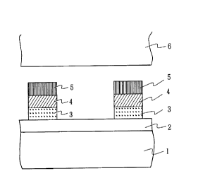
BRIEF DESCRIPTION OF THE DRAWING
Figure 1 is a schematic sectional view showing an
embodiment of a transparent electromagnetic radiation
shield material according to the present invention and a
display to which it is attached.
SUM~ZARY OF THE INVENTION
The present invention overcomes the aforesaid
problem of poor clarity owing to reflection when the side
facing the display exhibits metallic glare and the
aforesaid problem of the conductivity (electromagnetic wave
radiation shielding performance) being degraded by
oxidation of the metallic layer during use of the
electromagnetic radiation shield material (in air). The
present invention is characterized in further laminating a
second black layer on the metallic layer.
Specifically, in a first aspect, the present
invention provides a transparent electromagnetic radiation
shield material comprising a transparent base material, an
- 5 -
CA 02297335 2000-O1-27
optional transparent adhesive layer on the transparent base
material, and a first black layer, a metallic layer and a
second black layer of identical mesh pattern successively
laminated in alignment on the transparent base material,
directly or via the optional transparent adhesive layer, a
portion of the second black layer being removed as
required.
In a second aspect, the present invention
provides a transparent electromagnetic radiation shield
material according to the first aspect, wherein the mesh
pattern is a grid pattern of lines of a width of 50um or
less, interval (opening width) of less than 200um and
thickness of 50um or less.
In a third aspect, the present invention provides
a transparent electromagnetic radiation shield material
according to the first aspect, wherein the first black
layer and the second black layer are black metallic oxide
layers.
In a fourth aspect, the present invention
provides a method of producing a transparent
electromagnetic radiation shield material comprising an
optional step of forming an optional transparent adhesive
layer on a transparent base material, a step of
successively forming on the transparent base material,
directly or via the optional transparent adhesive layer, a
first black layer selected from among a black resin layer,
a black inorganic layer and a black metallic oxide layer,
- 6 -
CA 02297335 2000-O1-27
a metallic layer, and a second black layer selected from
among a black resin layer, a black inorganic layer and a
black metallic oxide layer, a step of providing a mesh-like
resist layer on the second black layer, a step of removing
portions of the first black layer, metallic layer and
second black layer not protected by the resist layer by
sand-blasting and/or dissolution with an etching solution
to form a mesh pattern corresponding to the mesh-like
resist layer, and an optional step of peeling off the
resist layer and/or coating the mesh-like pattern side
(side opposite the transparent base material) with
transparent resin.
In a fifth aspect, the present invention provides
a method of producing a transparent electromagnetic
radiation shield material according to the fourth aspect,
wherein the metallic layer is formed by direct
electroplating on the first black layer having a surface
resistance of 102 or less.
In a sixth aspect, the present invention provides
a method of producing a transparent electromagnetic
radiation shield material according to the fourth aspect,
wherein the black metallic oxide layer is formed by one or
a combination of two or more processes selected from among
ion plating, sputtering, vacuum deposition, electroless
plating and electroplating.
In a seventh aspect, the present invention
provides a method of producing a transparent
CA 02297335 2000-O1-27
electromagnetic radiation shield material comprising a step
of forming resist on a transparent base material in a
reverse-mesh pattern, a step of successively forming
thereon (on the surface of the transparent base material
portion and the resist portion) a first black layer, a
metallic layer and a second black layer, and a step of
removing only the first black layer, metallic layer and
second black layer on the resist portion surface by peeling
off the resist (liftoff process).
In an eighth aspect, the present invention
provides a method of producing a transparent
electromagnetic radiation shield material according to the
seventh aspect, wherein the first black layer and the
second black layer are black metallic oxide layers.
In a ninth aspect, the present invention provides
a method of producing a transparent electromagnetic
radiation shield material according to the seventh aspect,
wherein the total thickness (line thickness) of the first
black layer, metallic layer and second black layer is 5~m
or less.
DETAILED DESCRIPTION OF THE PREFERRED EMBODIMENTS
The base material used in this invention is
selected based on intended purpose. It is required to be
transparent. It is selected according to intended use from
among various materials including, for example, glass
_ g _
CA 02297335 2000-O1-27
plate, plastic film, plastic sheet and plastic plate. The
shape of the base material is not particularly limited.
When the transparent base material is a
continuous web (roll) of film, sheets of different sizes
can be easily cut from the obtained transparent
electromagnetic radiation shield film while avoiding
inclusion of defective portions. This is advantageous from
the points of high yield and economy. Since the roll film
can be produced by a continuous process, its productivity
is higher than when the transparent base material is plate-
like. Owing to its flexibility, moreover, the film can also
be used to produce curved shields.
The present invention also enables fabrication of
a transparent electromagnetic radiation shield panel by
laminating the transparent electromagnetic radiation shield
film by its electromagnetic wave shielding layer surface to
a display panel or a transparent base plate, using an
intervening transparent adhesive.
A plastic used as the base material is preferably
a resin with high transparency. Preferable examples include
acrylic resins, polycarbonate, polyethylene, AS resins,
vinyl acetate resin, polystyrene, polypropylene, polyester,
polysulfone, polyethersulfone, polyvinylchloride, olefine
maleimide copolymer, and norbornene resins. Among these,
olefine-maleimide copolymer and norbornene resins are
particularly preferable owing to their high heat
resistance.
_ g _
CA 02297335 2000-O1-27
The plastic should preferably have a thermal-
deformation temperature of 140-360°C, a coefficient of
thermal linear expansion of not greater than
6.2x10'SCm/cm.°C, a pencil hardness of not less than 2H, a
bending strength of 1,200-2,OOOkgf/cm2, a modulus of
elasticity in bending of 30,000-50,OOOkgf/cm2, and a tensile
strength of 700-1,200kgf/cm2. A plastic with these
properties is resistant to high-temperature warping and
scratching, and can therefore be used in a wide range of
environments.
The plastic preferably has an optical
transmittance of not less than 90~, an Abbe's number of
50-70 and a photoelasticity constant (glass region) of an
absolute value of not greater than 1Ox10'l3cmz/dyne . A
plastic with these properties exhibits high transparency
(is bright) and little birefringence (is not likely to
produce a double image), and therefore does not degrade the
image quality, brightness etc. of the display.
The metallic layer sandwiched between the first
black layer and the second black layer in this invention is
not particularly limited regarding type, color,thickness or
method of formation insofar it imparts electromagnetic
radiation shielding capability and can be etched.
Preferable examples include copper, nickel, iron, stainless
steel, titanium, aluminum, gold and silver of a resistivity
of l.OxlO'QS2cm or less. Among these, copper is particularly
preferable from the points of shielding property
- 10 -
CA 02297335 2000-O1-27
(resistivity), etchability and price. In general, the
shielding performance of the metallic layer improves with
increasing conductivity (smaller specific resistance), the
shielding performance thereof improves with increasing
thickness, and the etchability thereof improves with
increasing thinness.
Good shielding performance and etchability are
hard to achieve simultaneously when the resistivity exceeds
1 . OxlO'9C2cm.
The metallic layer can be formed by one or a
combination of two or more of ion plating, sputtering,
vacuum deposition, electroless plating and electroplating
as appropriate for the required thickness, adhesion and the
like. Otherwise a metallic foil can be used. Copper is
preferably used in the form of copper foil from the
viewpoint of shielding performance and price.
In the case of a copper foil, since the shielding
performance does not change substantially at thicknesses of
Sum and above (thinnest developed product; thinnest
commercially available product being 9um), one of a
thickness of 5-35um ,preferably 9-l8um, is ordinarily used
in consideration of handling ease and cost per unit area
(l8pm copper foil currently being cheapest).
The pattern and aperture ratio of the metallic
foil are not particularly limited insofar as they are
within ranges ensuring sufficient electromagnetic radiation
shielding performance and optical transmittance. Even a
- 11 -
CA 02297335 2000-O1-27
parallel line pattern, for example, provides shielding
effect (exhibiting directionality in the near field). Since
the effect is insufficient, however, a mesh pattern is
ordinarily used. Various basic mesh patterns are available,
including grid (tetragonal), triangular, polygonal,
circular and elliptical.
The aperture ratio (the ratio of the non-metallic
foil portion area relative to the repeated pattern unit
area) is determined by the line width and interval (opening
width) of the metallic layer. Different patterns with the
same aperture ratio have the same optical transmittance.
Since the electromagnetic radiation shielding performance
increases with decreasing opening width, however, a
narrower opening width is ordinarily preferable.
In thF case of a grid, the opening width is
preferably 200um or less, more preferable 100um or less.
The opening width can be reduced to any value within the
range in which patterning is possible. Therefore, no lower
limit is defined. In consideration of the lower limit of
the line width, the aperture ratio and the like, however,
the opening width is generally around lO~Zm at the smallest.
When the opening width is expanded, the shielding
performance always decreases if the aperture ratio (optical
transmittance) is increased. When the opening width is
narrowed, enhanced shielding performance can be achieved
simultaneously with an increase in the aperture ratio
(optical transmi~~aance) .
- 12 -
CA 02297335 2000-O1-27
The line width is preferably 50um or less, more
preferably 25um or less. Setting the opening width and the
aperture ratio automatically sets the line width. No
particular lower limit is set for the line width. In
consideration of patternability and the like, however, the
line width is generally around 2um at the smallest.
The line thickness is preferably 50um or less,
more preferably 25~,un or less. In consideration of
patternability, viewing angle and the like, the aspect
ratio (line thickness/line width) is ordinarily set at 1 or
less (because patternability decreases and viewing angle
narrows with increasing aspect ratio). No particular lower
limit is set for the line thickness. In consideration of
shielding performance and the like, however, the line
thickness is generally around lum at smallest.
The final values are, however, decided to fall
within ranges that do not cause occurrence of Moire fringes
when the transparent electromagnetic radiation shield
material is disposed on the front of the display panel.
In the present invention, each black layer is one
or a combination of two or more of a black resin layer, a
black inorganic layer and a black metallic oxide layer.
The black layers are formed to obtain clarity
(viewability), including such aspects of clarity as
antireflection property and the like. Figure 1 shows the
transparent base material disposed in front of a display 6.
The first black layer visible through the transparent base
- 13 -
CA 02297335 2000-O1-27
material must have a high degree of blackness. The second
black layer, however, requires only such a degree of
blackness as not to exhibit metallic glare and cause
reflection. (This will be explained in more detail later.)
When the first black layer is directly
electroplated, the conductivity of the first black layer as
expressed in surface resistance must be lOS2 or less
(explained later). In other cases, only a degree of
blackness is required and conductivity is unnecessary (but
not a problem if present).
(1) In the case of the black resin layers, the
first black resin layer (on the side nearer the transparent
base material) i.s a resin layer containing black pigment
and the second black resin layer (on the side farther from
the transparent base material) is a resin layer containing
a black pigment and/or a black dye.
Black pigment, which is high in blackness level
and stability, is used in the first black resin layer to
ensure a sufficient degree of blackness of the black layer.
(Black dye cannot be used owing to its low blackness level
and stability.)
Either black pigment or black dye can be used for
the second black resin layer because it is only required to
prevent reflection.
The black pigment used must exhibit black color.
It can, for example, be composed of reduced metal
particles, metal oxide particles, carbon particles or the
- 14 -
CA 02297335 2000-O1-27
like. The reduced metal particles can be colloid particles
contained in a reduced metal colloid dispersion or reduced
metal powder particles obtained from the metal colloid
dispersion. They are not particularly limited as regards
type of metal or grain size insofar as they are uniformly
dispersible in the coating liquid (coating). To ensure
dispersion stability, however, the grain size is preferably
lum or less . The reduced metal particles preferably have
high stability with respect to the atmosphere and moisture.
Specific examples include colloids containing
metals belonging to Group Ib or Group VIII of the Periodic
Table of the Elements (Cu, Ni, Co, Rh, Pd etc.), with
reduced Ni colloid particles and reduced Ni powder obtained
therefrom being particularly preferable. The reduced metal
colloid particles can be produced by the methods described
in Japanese Patent Application Laid-Open No. 1-315334.
Specifically, a colloid dispersion can be obtained by
reducing a salt of the metal in a mixed solution consisting
of a lower alcohol and an aprotic polar compound.
Like the reduced metal particles, the metal oxide
particles are also not particularly limited as regards type
of metal or grain size insofar as they are uniformly
dispersible in the coating liquid (coating). To ensure
dispersion stability, however, their grain size is
preferably l~.un or less. Preferable examples include
particles of oxides of metals belonging to Group Ib or
- 15 -
CA 02297335 2000-O1-27
Group VIII of the Periodic Table of the Elements such as
iron, copper, nickel, cobalt and palladium.
Like the reduced metal particles and the metal
oxide particles, the carbon particles are also not
particularly limited as regards type or grain size insofar
as they are uniformly dispersible in the coating liquid
(coating). To ensure good dispersion stability, however,
their grain size is preferably lum or less. Preferable
examples include carbon black and particles of natural or
artificial graphite.
The black dye used is not particularly limited as
regards type or content insofar as it is uniformly
dispersible or soluble in the coating. When present in the
coating, the black pigment is preferably stable against the
atmosphere, moisture, light and heat. Specific examples
include acid dyes, dispersion dyes, direct dyes, reactive
dyes, sulfur dyes, sulfur vat dyes and the like. Among
these acid dyes are particularly preferable.
The amount of the black pigment or black dye
contained in the black resin layer is preferably 1-80wt~,
more preferably 5-70wtg. At a content of less than lwt$,
the degree of blackness of the black layer is low. At a
content of greater than 80wt~, the physical properties of
the coating are degraded.
The resin used in the black resin layer can be of
any type capable of efficiently dispersing or dissolving
the black pigment or black dye in the resin solution (black
- 16 -
CA 02297335 2000-O1-27
coating liquid) containing the black pigment or the black
dye in dispersion or solution and in the coating (black
resin layer) obtained by applying and drying the coating
liquid.
The resin can be of any degree of transparency,
color and the like insofar as it does not impair the
blackness of the black resin layer (the degree of blackness
of the black layer).
Specific examples of preferable resins include
polyvinyl acetal, acrylic, polyester, cellulose, polyimide
and gelatin resins.
The black resin layer referred to here is a black
layer whose constituent other than the black pigment or
black dye (matrix or binder) is totally resin. Plasticizer,
surfactant and other additives can be included to the
extent that they do not degrade the physical properties of
the black resin layer.
In addition to being black, the first black resin
layer is also electrically conductive owing to its high
content of black pigment such as conductive carbon
particles (soot, carbon black, graphite or the like) and
reduced metal colloid particles (or reduced metal powder
obtained therefrom). It can therefore be directly
electroplated. Because of this, the conductivity of the
black resin layer expressed in surface resistance is
preferably lOf2 or less, more preferably 5S2 or less . When
- 17 -
CA 02297335 2000-O1-27
the surface resistance is greater than lOS2, the deposition
of the plating lacks uniformity.
For this purpose, an ink-like liquid obtained by
dispersing carbon particles in a resin solution (carbon
content of coating after drying about 90~), a conductive
carbon paint, or a resin solution containing dispersed
palladium colloid particles or the like can be used to
advantage.
In the case of using reduced metal colloid
particles, a black resin layer that is capable of being
directly electroplated (that is conductive) can also be
formed by forming a transparent resin layer and then
soaking it in a reduced metal colloid particle dispersion
(causing the reduced metal colloid particles to permeate
into and adsorb on the transparent resin layer.) When this
method is used, the reduced metal colloid particle content
of the black resin layer obtained exhibits a gradient in
the thickness direction of the resin layer (content
greatest at the surface layer) . This method is, however,
highly effective for obtaining excellent electroplating
deposition property and adhesion property.
Although the processing conditions vary depending
on the type, concentration and colloid grain diameter of
the metal of the reduced metal colloid dispersion, in the
case of commercially available standard palladium
dispersion (containing about 1~ Pd as PdCl2), soaking is
conducted for 1-60min, preferably 5-30min, at normal room
- 18 -
CA 02297335 2000-O1-27
temperature. At less than lmin the degree of blackness and
conductivity are low (plating deposition uneven). When the
soaking time exceeds 60min, little additional increases in
the degree of blackness and the conductivity are observed.
Although direct electroplating of a conductive
black layer has been practiced in the past, it has been
used solely in applications requiring only conductivity
(not requiring blackness), such as in the case of printed
circuit board through-hole plating and the like.
In this invention, it is used in applications
requiring a black layer (blackness), and the fact that the
conductive black layer can be directly electroplated is
utilized to simplify the production process and reduce
cost, which is totally new as a method of producing a
transparent electromagnetic radiation shield material. This
method is highly effective for producing high-performance
transparent electromagnetic radiation shield materials at
low cost.
The solvent for preparing the black coating
liquid resin solution in this invention can be of any type
insofar it can disperse or dissolve the resin and the black
pigment or black dye.
Preferable solvents include one or a mixture of
two or more of, for example, water, methanol, ethanol,
chloroform, methylene chloride, trichloroethylene,
tetrachloroethylene, benzene, toluene, xylene, acetone,
ethyl acetate, dimethylformamide, dimethylsulfoxide,
- 19 -
CA 02297335 2000-O1-27
dimethylacetamide and N-methylpyrrolidone. A solvent
appropriate for the combination of resin and black pigment
or black dye is selected.
The amount of solvent used is selected so as to
obtain an appropriate viscosity and fluidity and to make
the solution appropriate for application to the base
material.
The solution of the resin and black pigment or
black dye (black coating liquid) is applied to the
transparent base material or the metallic layer and dried
to form a coating (black resin layer) containing the black
pigment or black dye. The application of the solution can
be carried out by brush coating, spraying, dipping, roller
coating, calender coating, spin coating, bar coating,
screen printing or other conventional method selected in
view of the shape of the transparent base material or
metallic layer.
The conditions (temperature, time etc.) for
coating formation are determined based on the type and
concentration of the resin, the coating thickness and the
like. The nonvolatile content of the solution is normally
0.05-20wt$. The thickness of the dried coating is 0.5-50um,
preferably 1-25~.un. No blackness is observed and the clarity
is poor at a thickness of less than 0.5~,un. The viewing
angle is narrow at a thickness exceeding 50um.
- 20 -
CA 02297335 2000-O1-27
(2) When the first black layer and the second
black layer are formed as black inorganic layers they are
both inorganic layers containing black pigment.
The black pigment used is not particularly
limited as regards type or grain size insofar as it is
uniformly dispersible in the black inorganic layer. To
ensure good dispersion stability, however, the grain size
is preferably lum or less. The same black pigments as set
out regarding the black resin layer can be used.
The amount of the black pigment contained in the
black inorganic layer is preferably 1-50wt$, more
preferably 5-25wt~. At a content of less than lwt~, the
degree of blackness of the black layer is low. At a content
of greater than 50wt~, the physical properties of the black
layer are degraded.
To form the black inorganic layer, inorganic
particles containing black pigment and/or a mixture of
black pigment and inorganic particles are made into a
liquid or pasty black coating liquid together with a fluid
substance, the black coating liquid is applied and dried to
form a coating, the coating is heat treated as required,
and the particles are bonded by fusion, sintering or use of
a binder.
The inorganic particles used are not limited by
type, grain size, transparency, color or the like insofar
as they can be uniformly dispersed in the liquid or pasty
black coating liquid and do not degrade the blackness of
- 21 -
CA 02297335 2000-O1-27
the black inorganic layer. To ensure good dispersion
stability, however, the grain size is preferably lum or
less. Although the inorganic particles are used chiefly for
forming the matrix, they are also used to impart viscosity
and thixotropy to the black coating liquid.
Preferable inorganic particles include single arid
multiple component oxides such as silicate glass (Si02),
alkali silicate glass (NazO-SiOz). soda-lime glass (Na0-Ca0-
SiOz) , potassium-lime glass (Kz0-Ca0-SiOz) , lead glass (Kz0-
l0 Pb0-SiOz) . barium glass (Ba0-Bz03-SiOz) , borosilicate glass
(NazO-BZOs-SiOz) , other glasses (main components shown in
parentheses), A12~3, TiOz, ZrOz, Mg0 and the like, carbides
such as SiC, WC, TiC, TaC, ZrC, BaC and the like, nitrides
such as SisNa, TiN, ZrN, A1N and the like, oxynitrides
BN,
such as sialon and the like. The different types of
inorganic particles can be used individually or in
combinations. Am~~ng them, soda-lime glass is particularly
preferable.
The fluid substance can be composed of solvent
alone but is ordinarily composed of solvent and binder
remaining as a solid component after black inorganic layer
formation.
The binder is dissolved resin'or dispersed resin
particles or inorganic particles in the fluid substance.
The inorganic particles for the binder have a lower melting
point and smaller content than the inorganic particles for
the matrix. The inorganic particles for the binder are not
- 22 -
CA 02297335 2000-O1-27
distinguished from the inorganic particles for the matrix
in other respects.
On the other hand, the resin used as binder is
not particularly limited by type insofar as the black
pigment and the inorganic particles can be efficiently
dispersed therein in the state of the black coating liquid
and the black inorganic layer. The matrix and binder resins
set out for the black resin layer can be used. However, to
ensure the required physical properties (hardness etc.) and
l0 workability of the inorganic layer, the binder resin is
used in the black inorganic layer at a content of lOwt$ or
less.
The black resin layer has high coating
formability (particularly in the case of a thin film) but
is low in patternability by a process such as blasting (the
coating is softer than the black inorganic layer). The
opposite can be said of the black inorganic layer, which
has markedly different properties from the black resin
layer. Selection is therefore made between the black resin
layer and the black inorganic layer based on the required
mesh pattern, line width/line interval (opening width),
viewing angle, fabrication precision, fabrication cost and
the like.
The solvent used can be of any type insofar it is
capable of dispersing or dissolving the black pigment,
inorganic particles and binder. The same solvents as set
out regarding the black resin layer can be used.
- 23 -
CA 02297335 2000-O1-27
The nonvolatile component concentration of the
black coating liquid, the thickness and coating method of
the black inorganic layer and the like are the same as in
the case of the black resin layer.
The black inorganic layer referred to here is a
black layer whose inorganic component accounts for greater
than 50wt$ of the components other than black pigment
(matrix or binder). Irrespective of the content of
components other than the black pigment in the black
inorganic layer, when they constitute the "sea" portion of
a "sea/island" structure they are referred to as the
"matrix," as distinguished from the "binder" in other
cases. Plasticizer, surfactant and other additives can be
included to the extent that they do not degrade the
physical properties of the black inorganic layer.
(3) In the case of a black metallic oxide layer
(black metallic oxide being defined to mean not "oxide of
black metal" but "black oxide of metal"), as in the case of
the black resin layer and the black inorganic layer, the
layer is one added to (laminated on) the metallic layer and
is not a layer formed by blacking a portion (surface layer)
of the metallic layer by oxidation processing.
Any black metallic oxide having sufficient
blackness and capable of etching can be used irrespective
of type, thickness or forming method.
Preferable examples include oxides of copper,
nickel, cobalt, iron, palladium, platinum, indium, tin,
- 24 -
CA 02297335 2000-O1-27
titanium, chromium and the like. Such oxides can be used
individually or in combinations of two or more. Among them,
copper oxide and tin oxide are particularly preferable from
the aspects of etching workability and price.
Some metallic oxide layers (mostly ones with
electrical insulating property) have low conductivity
(e. g., one made of tin oxide etc.). Such metallic oxide
layers cannot readily provide good shielding performance
and are clearly distinguished from a metallic layer as
regards purpose and conductivity.
The thickness of the black metallic oxide layer
is preferably 0.01-l~un, more preferably 0.05-0.5um. At less
than O.Olum, many pinholes occur and blackness is
insufficient. At greater than lum, the processing cost is
high.
The black metallic oxide layer can be formed by
one or a combination of two or more of vacuum deposition,
sputtering, ion plating, electroless plating and
electroplating.
When the first black layer is laminated on the
transparent base material through an intervening
transparent adhesive, the transparent adhesive can be
selected from among, for example, polyvinylacetal, acrylic,
polyester, epoxy, cellulose and vinyl acetate type
adhesives. The thickness of the adhesive layer is generally
lum or greater, preferably about 5-500um.
- 25 -
CA 02297335 2000-O1-27
As viewed from the side of the transparent base
material (thickness: 2mm, refractive index: 1.49, optical
transmittance: 93~, average roughness Ra: 4010 of the
laminated article, the first black layer preferably has a
degree of blackness, expressed as optical density, of 2.9
or greater (angle of incidence of 7 °; assuming no specular
component). When the optical density is less than 2.9,
clarity of the final transparent electromagnetic radiation
shield material is poor owing to the low degree of
blackness. (The intensity of metallic glare increases with
decreasing optical density.) When the optical density is
2.9 or greater, the degree of blackness is sufficiently
high but the clarity by this alone is not adequate. Fully
satisfactory clarity is obtained only after the second
black layer having an optical density of 2.7 or greater is
overlaid. In the laminated product overlaid with the second
black layer, clarity as perceived by the naked eye does not
improve substantially when the degree of blackness of the
first black layer expressed as optical density exceeds 4Ø
Although the three layers (the first black layer,
metallic layer and second black layer) stacked on the
transparent base material, directly or through an
intervening transparent adhesive layer, can be given
identical aligned mesh patterns by direct processing with
a laser beam or the like after overlaying the third layer
(second black layer), ordinarily either (A) blasting and/or
etching or (B) liftoff is used for this purpose.
- 26 -
CA 02297335 2000-O1-27
(A) In the case of blasting and/or etching, a
mesh-like resist portion is first formed on the second
black layer after forming the three stacked layers. The
resist portion can be formed by a generally known method
such as printing or photolithography.
The second black layer is then formed into a mesh
pattern corresponding to the resist portion. The method
used for is selected according to the type of black layer.
For instance, blasting or the like can be used when the
black layer is a black resin layer or black inorganic
layer, and etching (dissolution with an etching solution)
or the like (for removing non-resist portions) can be used
when the black layer is a black metallic layer. The mesh-
like second black resin layer can also be formed by (1)
directly printing black resist in a mesh pattern or (2)
exposing and developing a black photoresist to impart a
mesh pattern. The metallic layer is then formed into a mesh
corresponding to the resist portion. Etching like that used
for the black metallic layer can be used for this. .
Next, the first black layer is formed into a mesh
pattern corresponding to the resist portion. As in the case
of the second black layer, this can be carried out by
blasting, etching or the like. When the first black layer
is a first black resin layer containing carbon particles
and has conductivity (surface resistance) enabling anodic
oxidation and the metallic layer is composed of a metal
(such as A1) which when subjected to anodic oxidation forms
- 27 -
CA 02297335 2000-O1-27
an oxide film at the metal surface layer, the carbon
particles in the first black resin layer are made brittle
by the anodic oxidation and fall off (accompanied by the
resin). Anodic oxidation is therefore effective as a method
for removing the first black resin layer at the non-resist
portions.
Finally, the resist portion is removed by, for
example, soaking in an exfoliating solution such as an
aqueous alkali solution.
When the first black layer is processed by
blasting, the surface of the transparent base material or
the transparent adhesive layer at the non-resist portions
is roughened (whitened) and is therefore preferably coated
with a transparent resin to restore transparency.
The blasting and etching conditions are not
particularly defined but can be chosen as appropriate for
the type of black layer and metallic layer.
(B) In the case of liftoff, resist is formed on
the transparent base material in a reverse-mesh pattern
before forming the three stacked layers. Then, after the
three layers have been overlaid on the transparent base
material and the resist, the resist (with the three layers
thereon) is peeled off to leave three mesh-like layers on
the transparent base material. The method and conditions of
forming the resist pattern portion and the peeling method
and conditions are the same as those in the case of
blasting and/or etching.
- 28 -
CA 02297335 2000-O1-27
By liftoff, the formation of the three layers
into a mesh pattern can be achieved merely by peeling off
the resist of reverse-mesh pattern (with the three layers
thereon), with no need for blasting, etching or other such
processing. The resulting marked reduction in the number of
processing steps ensures higher processing precision and
yield than in the case of the method utilizing blasting
and/or etching.
To facilitate peeling/removal of the resist (with
the three layers thereon), the thickness of the three
layers should preferably be 5~un or less, more preferably
3~un or less. When their thickness exceeds Sum, portions of
the three layers at non-resist portions of the transparent
base material may also peel (poor processability). The
minimum thickness need not be limited from the processing
aspect (processability improves with increasing thinness)
but is determined by the required shielding performance. To
achieve a thickness of Sum or less, the first and second
black layer should preferably be black metallic oxide
layers because sufficient degree of blackness can be
secured with such layers even when thin. Black metallic
oxide layers are ordinarily deposited by a dry method such
as ion plating, sputtering or vacuum deposition, but can
also be formed by a wet method such as electroless plating
or electroplating.
In this way there is fabricated a transparent
electromagnetic radiation shield material having a mesh
- 29 -
CA 02297335 2000-O1-27
pattern of a metallic layer sandwiched between black layers
(the metallic layer being exposed at a grounding portion
for connection of an earth lead). Provision of the
grounding portion is required when the shield material is
installed on a display or the like. It can be provided by
using a commonly known method (blasting etc.) to remove a
portion of the second black layer (usually at the frame
portion) to expose the metallic layer (conductive portion).
The transparent electromagnetic radiation shield
material preferably has an optical transmittance of 65% or
greater and a shielding performance of not less than 40dB
in the range of 30 to 1000MHz (50dB or greater at 500MHz).
An optical transmittance of less than 65% is too dark and
a shielding performance of less than 40dB (30-1000MHz) is
not sufficient for practical applications.
When the foregoing production methods are applied
to a transparent film to fabricate a transparent
electromagnetic radiation shield film, the transparent
electromagnetic radiation shield film is thereafter
laminated to a display panel or a transparent base plate,
using an intervening transparent adhesive if necessary, to
fabricate a transparent electromagnetic radiation shield
panel. The transparent film is preferably one constituted
as a continuous web that can be continuously processed into
a roll. Such films include plastic films having a thickness
in the approximate range of 5-300~un made of polyethylene
terephthalate (PET), polyimide (PI), polyethersulfone
- 30 -
CA 02297335 2000-O1-27
(PES), polyether-etherketone (PEEK), polycarbonate (PC),
polypropylene (PP), polyamide, acrylic resin, cellulose
propionate (CP), and cellulose acetate (CA).
An example of a transparent electromagnetic
radiation shield material provided by the invention will
now be explained with reference to Figure 1. In the
illustrated example, the first black layer is a first black
resin layer containing dispersed black pigment, the
metallic layer is a metallic foil layer, and the second
black layer is a second black resin layer containing
dispersed or dissolved black pigment or black dye.
Figure 1 shows the sectional structure of the
shield material. The first black resin layer 3 and the
second black resin layer 5 are disposed to oppose each
other with the metallic foil layer 4 sandwiched
therebetween in a unitary, aligned mesh pattern.
The transparent base material 1 and the first
black resin layer 3 are attached through a transparent
adhesive 2. The transparent base material 1 and the first
black resin layer 3 can instead be directly adhered without
use of an adhesive. This can be achieved, for example, by
rolling, spraying or otherwise applying molten or dissolved
black resin on the transparent base material 1 and then
drying the applied coating.
The invention will now be explained more
specifically with reference to working examples.
- 31 -
CA 02297335 2000-O1-27
Example 1.
A black coating liquid was prepared by uniformly
dispersing black pigment (iron oxide fine powder; Tetsuguro
P0023, product of Daido Chemical Industry Co., Ltd.) in an
alcohol (ethanol) solution of polyvinylbutyral (PVB)
(#6000-C, product of Denki Kagaku Kogyo, Co., Ltd.).
(Coating solution composition (parts by weight): iron
oxide/PVB/ethanol = 50/100/1850.)
The coating liquid was applied to one surface of
12~.un electrolytic copper foil (CF T9 SV, product of Fukuda
Metal Foil and Powder Co., Ltd.) and dried to obtain a
first black resin layer (l0um). The coated surface was
laminated to a polyethylene terephthalate (PET) film
(Lumirror, product of Toray Industries, Inc.) using an
acrylic adhesive to obtain a laminated article.
A black photoresist (NPR-60/SCER, product of
Nippon Polytech Corp.) was applied to the copper foil side
of the laminated article as resist for processing the first
black layer and the metallic layer (iron oxide, 13$ in
dried coating), followed by prebaking, exposure,
development and post-baking to form a resist pattern
(second black resin layer; thickness, 20~un; grid pattern;
line width, 20um; line interval, 180um).
The black resist-patterned article was soaked in
etching solution (aqueous solution of 20~ ferric chloride
and 1.75 hydrochloric acid) to dissolve and remove the
copper foil layer at the non-resist portions, the first
- 32 -
CA 02297335 2000-O1-27
black resin layer was removed by sand blasting, and an
acrylic resin paint was applied and dried to afford a
transparent electromagnetic radiation shield material
(having the same patterning, line width and line interval
as the resist).
The electromagnetic radiation shield material
exhibited shielding performance of 65dB (500MHz) and
transparency (optical transmittance) of 75$. The degree of
blacknesses of the first black layer and the second black
layer were high, so that the shield material exhibited
excellent clarity with no reflection from the side facing
the display.
Example 2.
The second black layer of Example 1 was formed
not as a black resist pattern (second black resin layer)
but as a soda-lime glass inorganic layer containing
dispersed iron oxide fine powder (second black inorganic
layer, l0um) and further with a resist pattern (thickness:
l0um) and the second black inorganic layer was thereafter
processed (patterned) by sand blasting.
Next, as in Example 1, the metallic layer and the
first black resin layer were processed (patterned) by
etching and sand blasting to fabricate a transparent
electromagnetic radiation shield material. This
electromagnetic radiation shield material exhibited the
same excellent performances as that obtained in the Example
1.
- 33 -
CA 02297335 2000-O1-27
Example 3.
The second black layer of Example 1 was formed
not with the black resist pattern (second black resin
layer) but with a copper oxide layer (second black metallic
oxide layer) and further with a resist pattern and the
second black metallic oxide layer and the metallic layer
were thereafter processed (patterned) by etching.
Next, as in Example 1, the first black resin
layer was processed (patterned) by sand blasting to
fabricate a transparent electromagnetic radiation shield
material. This electromagnetic radiation shield material
exhibited the same excellent performances as the that
obtained in Example 1.
Examples 4-6.
The first black layers of Examples 1-3 were
formed not as resin layers containing black pigment (first
black resin layers) but as soda-lime glass inorganic layers
containing iron oxide fine powder (first black inorganic
layers ) .
Other aspects of the fabrication (patterning)
were conducted in the same manner as in Examples 1-3. The
transparent electromagnetic radiation shield materials
obtained exhibited the same excellent performances as those
obtained in Example 1.
Examples 7-9.
The first black layers of Examples 1-3 were
formed not as resin layers containing black pigment (first
- 34 -
CA 02297335 2000-O1-27
black resin layers) but as copper oxide layers (first black
metallic oxide layers). Further, the processing
(patterning) used for the first black layer of Examples 1-6
( first black resin layer or first black inorganic layer)
was adopted but etching was utilized in place of sand
blasting. The transparent electromagnetic radiation shield
materials obtained exhibited the same excellent
performances as those obtained in Example 1.
The combinations of first black layer, metallic
layer and second black layer in Examples 4-9 are shown in
Table 1.
Example 10.
A transparent electromagnetic radiation shield
material was fabricated whose second black layer was formed
by replacing black pigment (iron oxide fine powder)
contained in the second black resin layer of Example 1 with
black dye (metal-containing acid dye).
In clarity, this electromagnetic radiation shield
material rated "good," somewhat inferior to the "very good"
rating of the electromagnetic radiation shield material of
Example 1, but the other performances were substantially
the same as those obtained in Example 1.
Example 11.
A transparent electromagnetic radiation shield
material was fabricated whose metallic layer was formed by
replacing the copper foil (l2um) of Example 1 with aluminum
foil (l5um).
- 35 -
CA 02297335 2000-O1-27
In shielding performance, this electromagnetic
radiation shield material rated "good," somewhat inferior
to the "very good" rating of the electromagnetic radiation
shield material of Example 1, but the other performances
were substantially the same as those in Example 1. The
transparent electromagnetic radiation shield material of
this example is advantageous in terms of light weight and
low cost.
Example 12.
A transparent electromagnetic radiation shield
material was fabricated in the manner of Example 1 except
that an polymethylmethacrylate resin (PMMA) plate was used
in place of the PET film. The electromagnetic radiation
shield material exhibited the same excellent performances
as that obtained in Example 1.
Example 13.
A transparent electromagnetic radiation shield
material was fabricated by using ion plating (IP) to form
on a polycarbonate film, in sequence, IP copper oxide
(first black metallic oxide layer, 0.5um), IP copper
(metallic layer, 2~un) and IP copper oxide (second black
metallic oxide layer, 0.5~.un), forming a resist pattern, and
processing (patterning) all three layers at one time by
etching.
In shielding performance, this electromagnetic
radiation shield material rated "good," somewhat inferior
to the "very good" rating of the electromagnetic radiation
- 36 -
CA 02297335 2000-O1-27
shield material of Example 1, but the other performances
were substantially the same as those obtained in Example 1.
The method of this example enables high-yield fabrication
of electromagnetic radiation shield materials with high
pattern resolution and degree of finish.
Example 14.
A transparent electromagnetic radiation shield
material was fabricated whose metallic layer was formed by
replacing the copper foil (l2um) of Example 1 with
electroless copper (metallic layer, 2uln) provided by
electroless copper plating. (After the first black resin
layer had been formed on one side of the PET film, it was
imparted with a plating catalyst and the electroless copper
was then formed thereon by electroless copper plating.)
In shielding performance, this electromagnetic
radiation shield material rated "good," somewhat inferior
to the "very good" rating of the electromagnetic radiation
shield material of Example 1, but the other performances
were substantially the same as those in Example 1.
Example 15.
The first black layer of Example 1 was formed not
as a black resin layer containing dispersed iron oxide fine
powder but as a conductive black resin layer (first black
resin layer) by (1) applying and drying a conductive paint
containing carbon (mainly graphite) particles dispersed in
a resin solution (Everyohm lOlS, product of Nippon Graphite
Industries Ltd.) or (2) forming a coating of clear resin
- 37 -
CA 02297335 2000-O1-27
[polyvinylbutyral (PVB) (#6000-C, product of Denki Kagaku
Kogyo, Co., Ltd.], blackening the coating by immersing the
coating (for 30min at normal room temperature) in a black
reduced palladium (Pd) colloid dispersion liquid (OPC-80
Catalyst M, product of Okuno Chemical Industries Co.,
Ltd.), and further effecting conductor-conversion treatment
(by immersion for l5min at normal room temperature in a
mixed aqueous solution of Selector A and Selector B,
products of Okuno chemical Industries Co., Ltd.) and, if
necessary, drying. The metallic layer was formed by
replacing the copper foil (l2um) with electroplated copper
(metallic layer, 2um) formed by direct electroplating,
thereby fabricating transparent electromagnetic radiation
shield materials.
In shielding performance, these electromagnetic
radiation shield materials rated "good," somewhat inferior
to the "very good" rating of the electromagnetic radiation
shield material of Example 1, but the other performances
were substantially the same as those in Example 1.
In the case of (2), a similar electromagnetic
radiation shield material can be fabricated by extracting
and removing only the black component (Pd colloid
particles) from the first black resin layer by use of an
etching solution or the like (to make only the extracted
and removed portion transparent).
- 38 -
CA 02297335 2000-O1-27
Examples 16 & 17.
Transparent electromagnetic radiation shield
materials were fabricated in the manner of Example 13, with
the aperture ratio of the grid pattern (line width, 20~zm;
line interval, 180um; aperture ratio, 81~) left unchanged
but with the line width and line interval narrowed to 1/2
(Example 16) and 1/4 (Example 17).
With these electromagnetic radiation shield
materials (Examples 13, 16 and 17), shielding performance
tended to increase with narrower line interval (opening
width) .
Example 18.
A transparent electromagnetic radiation shield
material (line width, Sum; line interval, 45um; aperture
ratio, 87~) was fabricated by increasing the aperture ratio
and narrowing the line interval and width of the grid
pattern of Example 13.
This electromagnetic radiation shield material
was superior to that of Example 13 in transparency (optical
transmittance) and shielding performance.
Example 19.
In order to fabricate a transparent
electromagnetic radiation shield material like that of
Example 13 using the liftoff process, resist was formed on
the film in a reverse-mesh pattern, the three layers were
laminated in the manner of Example 13, the result was
- 39 -
CA 02297335 2000-O1-27
immersed in a defoliating solution, and the resist (with
the three layers thereon) was removed by peeling.
This electromagnetic radiation shield material
was superior to that of Example 13 in degree of finish
(processing precision). Its other performances were the
same as that of Example 13. As the method of this example
involves many fewer processing steps and achieves higher
yield that of Example 13, it can provide a low-cost
product.
Comparative Example 1.
A transparent electromagnetic radiation shield
material was fabricated in the manner of Example 1 except
that the second black resin layer was omitted. The
electromagnetic radiation shield material exhibited
metallic glare on the side facing the display and a little
reflection could be observed. The clarity was therefore
inferior to that obtained in Example 1.
Comparative Example 2.
A transparent electromagnetic radiation shield
material was fabricated in the manner of Example 1 except
that the black pigment (iron oxide fine powder) contained
in the first black resin layer was replaced with black dye
(metal-containing acid dye). Not only were the problems
encountered in Comparative Example 1 again observed but the
degree of blackness of the first black resin layer was also
inferior to that of Comparative Example 1. The clarity was
therefore markedly inferior to that obtained in Example 1.
- 40 -
CA 02297335 2000-O1-27
Comparative Example 3.
A transparent electromagnetic radiation shield
material was fabricated in the manner of Example 13, with
the aperture ratio of the grid pattern left unchanged but
with the line width and line interval doubled (line width,
40um; line interval, 360~un; aperture ratio, 81~). The
shielding performance was markedly inferior to that
obtained in Example 13.
Comparative Examples 4 & 5.
Transparent electromagnetic radiation shield
materials were fabricated in the manner of Example 1, with
the aperture ratio of the grid pattern left unchanged but
with the line width and line interval doubled (Comparative
Example 4) and expanded 20 times (Comparative Example 5).
With these shield materials (Example 1, Comparative
Examples 4 and 5), shielding performance tended to diminish
with wider line interval (opening width).
- 41 -
CA 02297335 2000-O1-27
b
d
L s
cC
C x s s s _
..a
C E~
i
W
~'
d ~ x s s s s _
0 ~
z
00 ~ R
C/] ~
C.
~ s z s x - _
U
O a x x c x
#
d ..
a0 V m
.-r O s s s s s _
p ~ ~a
.o ~ ~t
m
V O s s s s z _
E'~ ~ C7
O
.' o ~ = z s _ s
d y
O ~ ~, ~ _ _ _ _ x
~
C ~. .-r
>
O
a
v
.
.
47 ~ n
_ _ _ _ _ _
N
V
V V
_
~C ~ C
o a~ o y
~, ~,
p .5 E ~ .a c
~ ~
> y q> r
V~r UC~ ~'C V~ ~U~ V J
v
O O ~ ~ '4 ~ 'C ~
V ~ i ~
C~ U d r. . U
> 'C C , O ~C O
> d iG
O ' >
O
, .C .C , ~ >, ~ ,~ ,~
>~;~ ~ ~ ~ ~ ,
b .: ~C x ~o ~o ~i ~O :. ~
.~ ~ ..~ ,~ ~o _'~ i
x ~ x ~
C G C C C O C C C O
x O r c~ s. d
O a~ O o
. CC .. ~ ~ V~O' ~
C
d d ~ ~ mp ~>,O d V
CU y C7 O ~ U y~
~ ~ G7 G7 C
~
.- y~ y7 O C7 Sr
. U~ v~ Ul ~"~ y U~ v~ s.
va ~ c. .~ o v~ v7 o ...,
~.. ~-.. U s~ _ U
~.. ~-,
c~ ~
C. x x x x _ _
~
Uw
m
s.
d d
~
_ b
s x ~ = = R V o
::
~C
.
.
.~ a a ~ ,~ :_
~ o d
o
h~ t~. 40C
r~ r~VJQ
.r ~ fs.,
GL .:7 G~ ~
w ~
r~".,
r~
"",
C~ s s s s s
~ d O y ~
E~ G ~ f3,
E
~ _d
k
W G ~ ~V cry ~' ~n t0 n
CA 02297335 2000-O1-27
v ~ d
c, - _ _ L c,
C'~
E E r-~,, E ~ E
C. G .-~,
L~ ~ .3 ~ 3 ~
W W ~~
W
eT
d
o ~ o _
~ = o ~ _ _ _
.
U
w
O GV O s ~ O
~ O ~ O s s s s s
U O s s s s
to L =
(~ G~ d
O
! t L ! Z
Z
00
i
Q y s
r
s~, ~
C y "~, pip z z _ _ z -
~
a . c > ...,
v
O ~O _ _ s _ _ _
i ~ GV n
r:
iw
O
CC
L
C
c~~a d ~" _ a~
d C
V
:
: ~ c mss.
~ S
j
'mss '~' .~.~ '~' ~ d '''
.V. U O p '''", -~ ~'
~ O '~ >.
>a
~
, V .
'~ ~~ ... , ..
..
~ G ~ ~ C ~ ~ ~
. _ . ,_., ,_
~ ,~ O OCJO C
OCC O C
C
O
.
d~~ yo ~i0~ ~iy d~C ~
dO 0 c
o
~ s . .
v~ ~ v~ ... v~ E v~ . v7 u
~, _. E tn E rr~
U ca c. ..." ~.
~-. ....
d '' ... s'' s. u~
~ s.
~
y~4 '3~ s s ~~ fl G~ UrO.
G " ' V_'
C7 ..r 3 _ G ~. d
r Q ~"'~''v O
~ ~w~ a ~
Cw ~
~ W~
N
d
a> -C r
.., ~'.' ~ C
~p . .
.0
V O V V O _
~ d V
d ~7
7.. V
,~, ~ s ~ s s C
O ~,,
"C
'~' V '..T '~' .~'
~"' ~" :-.
'~ p n
C7
a~ ..'f. . C v ~
~. W V
y
r.3 . Ul ~
~ d o L' . ._
w ~ ~ ~
~ ~ n
r_ G> >. ~ v >. L
_cC r- O ~ m
r~ ~ H O
~ L
W ..~ W Fy.l ~ ~
. L .~ n
I 1...1
1
.~ ~ y ~ sw ! i ~ ~ L~
R (~ s s s ~ , L:
~ y' C
~ y
.i
t
E-~ C ~ 0.. d w A, p.
C ~~
~ d
~ '~" ~ M ~'
w d 00 ~ ,..i ..w .r
CA 02297335 2000-O1-27
ae '~' w f" ~ a,
L CC ~ ~ V) ?
~ x o y
cc as cx , ,.,N
~ 3 g 3 x ~ ~
W W ~ Ll
C C
w ~ o os~ ~ os~ o
.~ ~
..
Ch ~ x x x x
U
w
o ~ O x x x x
O x x _ _
r V O x ~ O
CC 1
H G a~
O
x x
d ~ ~ y ~ ap 00
U ~ ~ " x 00
C '~
~' ~
_ .. C C
.~
... 7
GV O 1f~C''~ C~7
C
U
' ~
_
c~
C
d
_ _
U U
c C csr,)
C i" O
~ c
> '
a a >,
c~ , ~ a
~' "'O ,
~ Y~ V ~~
~ r ' r.
U ~ ~ ~ v
C U
U ~
C!~ '..~ .n ~ Cl~
C/~ -i
f O r
_~ U ,~ to tr
GaUa~ C,G x x x
G
47 O ~ C
~.r _",d.
Q
0
rG '. : W y .i'
G v G
r
7 ~7
d
b
'O
X
O
C ~ x x x
~ V d
~ o
-a -
o
~
J .5C '~' '' a~
UO U o a V
u1
y
CC d ~,
G~.~ ~. ~UP~.~G. E~n'~-."
~ .w a
d
o x x x
C G7 C7
y
E-r G a i1. G.
~
~ ca t 00 O'~
W G ,r r, .~ .H
CA 02297335 2000-O1-27
d ~ d d
a c
f4 s, s, yt E, ,~
C. C.
fr GS s CO Ch ~C W ~C W
~ ~
m
8 E 8y Ey E~
~ ~
~ a G c c
~ Q Cg 3o?3WCg~o23W
Q Cg~3W
t~~~W
..
d ~ = X ~ a ~O X
d ~ c d
a
U
w
O ~ d s O s s
.SC x., X
d ..~G
N it
N
a ~-o~ c~ ~ d O _
U O
CC fr
E"~ 4 d
to
O pip = s
tVr y ~
~ o
d
C y C 000 s ~ s O
~ "~ ~'
a.~ ?~E
E o
= Q, O
a ~; ~
0
V
o
_
z
~. _~
V L C) d
a~ ~ y '->
~ '_'S > .:
. f" IC
v
m'
C . ~.
.
O V O d O C
U C
Fw Lr
V ~ V V
G
c' s C, ~ _
~., n
~
G~ ~ .~..
~ ~" v ~ w
~
cat
V
~O
C4 ~, ~C .
O
U G7 V y DD v p V d
~
_C4 _CSS ~ ~ ~ ~'.
~. ~, V
,~ ~
w .~G .~ w C c~ ~~ c0 y C
a ~ ~ ~ O ~
~ ~ ~
ue
t ~ in a~ .. y ~
r _~ m p C ~ ~, v~ p
a ~ s
~ ~'
~
V
Lr '~ Gz~, GZ, f. CL E ~r
t ~ , . ~
r ~ ..
'O
V
V
. ~
.O s. ' : !:, bD
ci~ C
C~ C y y y E." s t,:. r - d
~ U ~ ~
E a .~ 8 .n
.
t
d
d 8
CO y X
G. a6 G7 ~~ ~V M
G
CA 02297335 2000-O1-27
Remarks:
1) Transmittance ($) at wavelength 550nm measured by
spectroanalyzer (W-240, product of Shimadzu Corp.
s 80~
0 , < 80~ - z 65$
o . < 65~ - Z 50$
X . < 50 ~
2) Optical density (angle of incidence of 7°; assuming no
specular component) measured by spectrophotometric
colorimeter (CMS-35SP), product of Murakami Color Research
Laboratory, Ltd.
o , ~ 2.9
o . < 2.9 - ~ 2.7
X . < 2.7
3) An overall evaluation was made based on such factors as
degree of blackness and reflection when the shield material
was actually placed in front of a display (with the second
black layer facing the display). The results were rated as
follows:
Very good ()
Very high degree of blackness of first black
layer and second black layer and absolutely no
annoyance from reflection
Good (o)
~ Very high degree of blackness of first black
layer and substantially no
- 46 -
CA 02297335 2000-O1-27
annoyance from reflection despite slightly low
degree of blackness of second black layer
Fair (o)
Very high degree of blackness of first black
layer and slight annoyance from reflection owing
fairly low degree of blackness of second black
layer
Poor (X)
Fairly low degree of blackness of first black
l0 layer and second black layer and considerable
annoyance from reflection
4) Electric field shielding performance (dB) at 500 MHz
measured by electromagnetic radiation shielding performance
tester (TR-17301, product of Advantest Corporation)
~ : Z 60dB
o . < 60dB - Z 50dB
o . < 50dB - z 30dB
X . < 30dB
The present invention provides the following
advantageous effects:
(1) Pattern design is subject to little restriction.
(2) The degree of blackness and resolution of the black
pattern on the transparent base material (first black
layer) side are high and the opposite side (second black
layer) is free of metallic glare, providing outstanding
- 47 -
CA 02297335 2000-O1-27
clarity. Long-term stability of these properties is excellent.
(3) An earth lead can be easily connected.
(4) Conductivity of metallic layer is high, particularly
when formed of metallic foil, giving a high shielding
effect, and high optical transmittance can be obtained
since the aperture ratio can be set high. The long-term
stability of these properties is excellent.
(5) The structure of a metallic layer sandwiched between
black layers provides a protective effect that prevents
degradation of metallic layer performance even under high-
temperature, high-humidity conditions. Stable
electromagnetic wave radiation shielding performance can
therefore be obtained.
(6) The viewing angle is wide.
(7) Yield is good because the sheets to be laminated to
transparent base plates can be cut to different sizes from
a web (roll) of the transparent electromagnetic radiation
shield film while avoiding inclusion of defective portions.
(8) Curved shields can also be produced.
- 48 -