Note: Descriptions are shown in the official language in which they were submitted.
CA 02298494 2000-O1-24
Structure of safety elements for documents and devices for the testing of
documents with said safety elements as well as procedures of application
This invention relates to the structure of safety elements for documents and
devices
for the testing of documents with said elements as well as procedures of
application
according to patent application DE 19T 18 916.4.
Until now documents including diffraction-optically effective safety elements
used to be
checked by costly optical test procedures. for instance, a test of documents
with
diffraction-optically effective safety elements or so-called OVDs (optical
variable
device) is impossible within a document handling machine since it runs at very
high
speeds. DE 27 47 158 specifies a procedure and a test instrument for the
counterfeit
test of holographically secured identity cards. The OVD is reproduced and then
visually
checked. This procedure is not suitable for a fast, efficient, person-
independent test. 1n
EP 0 042 946 a device for the production of scanning patterns that are tested
by
means of laser, mirror and line systems as well as a photo detector is
specified. The
economic expenses are also very high in this case. (t would even be higher if
the -
rnaterial to be tested shall be tested unsortedly. In order to avoid a
presorting process a
multiple arrangement of counterfeit test systems or a repeated test would be
necessary.
CA 02298494 2000-O1-24
~2-
In EP 0 092 691 A1 a device for the detection of security strips in bank notes
is
specified. By means of two transmitted-light measuring channels in the
infrared range
and at wave lengths of about 5 pm the material-specific absorption bands of a
plastic
safety strip are measured. A counterfeit or quality test of diffraction-
optically effective
safety elements that reflect metatlically, such as reflex holograms or
kinegrarns, is not
.., specified in said EP and would not be possible by said device. From GB 21
64 644 A it
is known that a reflected-light procedure of bank notes is tested by means of
a line
scan camera, and from CH-PS 652 355 it is known that cards with a special
layer
structure are tested by means of a reflected-light procedure or transmitted-
light
procedure. In both cases it is a test in which received image information is
compared
with the originals. The reflections and traces of use appearing on both
versions are a
problem and a big disadvantage. An automatic counterfeit test of hotogam
information
is specified in DE-OS 38 11 905. For the reflected-light hologram test the
arrangement
specified in the DE--QS provides that the transmitter and the receiver shat(
be arranged
,~,, directly opposite to each other in order to be able to analyse the
hologram information.
This opposite arrangement of the transmitter and the receiver results in a
metrologically
disadvantageous overriding and sometimes even in a damage of the receiving
elements by a direct light incidence in the interspaces between the successive
bank
notes. When testing used bank notes existing creases make a test practically
impossible because of accidental reflections.
CA 02298494 2000-O1-24
-3 -
According to the known procedures specified above an exact positioning of the
objects
to be tested is required, and all devices are not suitable for high-speed
handling
machines.
In DE 196 04 856 A1 it is contemplated to carry out the condition, quality and
register
test of optical safety features in the form of metallically reflecting layers
such as
kinegrams, holograms and the like, on security papers, especially bank notes,
in such a
,~ way that a metallically reflecting safety feature of the security paper is
scanned by
transmitted light in an actually known way by means of at least one electronic
camera,
preferrably a CCD line scan camera, and that the actual values determined in
this way
are compared with the desired values by means of image evaluation methods
actually
known in order to mark bank notes having faulty safety features or to seperate
used
notes into a sorting unit. The device specified in DE 196 04 856 A1 is
characterized by
a transport system actually known to transport security papers within the
range of the
electronic camera, by an infrared radiation source on that side of the
security paper to
be tested which is opposite to the camera and that the optical axis of the
camera
includes an angle deviating from 180° with the optical axis of the
illumination unit, and
that the transport unit is preferrably set up by transport belts that are
spaced to each
other transversely to the transport direction.
This device or procedure has a disadvantage as well, such that especially used
bank
notes with creases or bank notes with a damaged kinegram film or a kinegram
film the
surface of which is contaminated are not detected as real bank notes. In
addition, the
specified procedure and the device relating to it are automated, however, they
are not
suitable for the high-speed bank note machines in circulation having a pass of
~ 1,200
notes per minute.
CA 02298494 2000-O1-24
-4-
piffraction-optically effective safety features or OVDs on security papers,
such as the
German 100 and 200 DM notes, are, at the moment, manually or visually tested
concerning damages, register accuracy, exact edge formation etc. The test is
carried
out visually during the bank note manufacture and, if necessary, during the
sorting out
of bank notes returning from circulation. This procedure is time-consuming and
costly.
In DE 195 42 995 A1, inter olio, a procedure for the counterteit test of a
data carrier by
adjusting the various data available is specified.
According to this patent specification there are the following possibilities:
- comparison of the standard image of the hologram with the one of the memory
unit,
- comparison of the hologram data of the hologram with the data within a
defined
range of the data carrier andlor those of a memory unit,
- comparison of the hologram data with the data available via an input unit,
- comparison of the individual image of the hologram with the data of the
input unit of
the memory unit andlor the data of the defined range.
This procedure is also time-consuming and costly. The testing is carried out
optically by
balancing via image detection by a reading device, and it is not suitable for
high-speed
,.r,
handling or testing machines.
In addition, inks are known as a test feature including special physical
features to
secure security documents and bank notes. It is possible to distinguish
between inks
that can be seen or felt visually without any aids and those that can only be
detected by
special aids depending on the respective physical property of the ink, such as
electric
conductivity or fluorescence.
CA 02298494 2000-O1-24
Interference inks belong to the group of inks that can be detected without any
additional aid. They can be found among the QM bank notes of the series from
1996 on
(1997 issue). When changing the examination angle a colour change can be
observed.
By this tilt effect a fast and uncomplicated manual single note test of bank
notes is
possible. Inks with flourescent or magnetic features or with a certain
electric
conductivity can only be detected by proper aids. Previous test devices,
however, have
a relatively low resolution and the corresponding safety features must have
large
dimensions in order to guarantee a good detectability.
When testing printing inks with different conductivities it proved to be a
disadvantage
that the different conductivities must be tested by different test devices in
the same test
process successively or in two test processes by the same test device given a
proper
software design. In addition, the measuring accuracy is low if the
conductivity of the
test field is low. It is not possible to test electrically conductive printing
inks with a
different electric conductivity due to their coating thickness and feature
substrates by
means of well-known test devices because of their tow resolution capacity.
The well-known features, test zones and test structures to be tested as well
as the~test
procedures and devices for the counterfeit test of objects, security papers,
especially
bank notes, have a major disadvantage which is their degree of being known.
This
degree pf being known makes it possible for the counterfeiter to draw
conclusipns from
the knowledge of the test procedures and devices and the way they work to the
features, test zones and test structures to be tested. This requires a
completely new
CA 02298494 2000-O1-24
formulation for the testing of objects, security papers, especially bank
notes, the
solution of which must be reflected in a new application system of test
features, test
procedures and test devices in order to avoid that information codes may be
easily
discovered and copied.
It is the object of this invention to overcome the disadvantages of the state-
of-the-art
"...,,, and to complete the structure of safety elements for documents by
additional safety
elements, and to contemplate devices for the testing of such safety elements
as well as
a new procedure of the application of safety elements and devices that make it
difficult,
if not even imposssible, for the counterfeiter to draw conclusions from the
functioning of
the test procedures and devices to the safety elements to be tested in order
to produce
counterfeits that are so similar to the originals that they are not detected
by the test
devices.
In addition, it is the object of this invention to contemplate diffraction-
optically effective
safety elements and features or OVps, respectively, that have to be precisely
tested in
", combination with electrically conductive printing inks quickly, person-
independent and
at low costs. The devices for the feature test belonging to it shall be used
in high-speed
document handling machines as well as in manual test devices. In addition, it
is the
object of this invention to design some of the devices relating to this
invention such that
they test a defined number of various safety elements or features existing on
a
document where the number of the safety elements to be tested varies between
the
devices. This object is directed to reaching different test criteria according
to the
potential expenses and testable safety elements.
CA 02298494 2000-O1-24
- 7_
This object is solved by the following invention specification.
The structure of safety elements for documents to be tested provides a new
design not
primarily based on a visual examination but on test procedures. This design --
hereinafter called functional design - is the combination of electrically
conductive and
isolating structures having the same or a different size, at the same or
different levels
to each other, with the same or different conductivities, and it is made of
metallized
structures andlor conductive inks or printing inks. In its variety and
composition the
functional design gets coding functions in aft distinguishable safety elements
and is,
thus, testable in a coded way. According to this invention the functional
design can be
a diffraction-optically effective safety element or it can consist of
electrically conductive
colours or inks. If it is designed as a diffraction-optically safety element
it can concur
with the optically, hence visually perceptible design and it can even support
it in its
optical design. Furthermore, it is possible to sputter the demetallized or non-
metallized
zones in order to upgrade the brilliance.
Today, holograms and other diffraction-optically effective safety elements for
the
securing of certificates and other security papers as well as bank notes for
the
prevention of counterteits are used more and more. Such documents are far
instance
bM bank notes of the 1996 series with a diffraction-optically effective safety
element in
the form of a kinegram in addition to the electrically conductive safety
strip.
CA 02298494 2000-O1-24
-$-
Electrically conductive printing inks are also welhknown. These inks are
included in the
different printing images, especially on bank notes, in structures of one test
feature,
and they don't allow any distinguishing or detection of the structures due to
their low
resolution. This increases the forgery-proof quality of the documents. For
instance, the
bank note numbering or other graphic details may consist of these inks.
Structures
according to this invention in test zones or printing images of electrically
conductive
,'~1
inks have, in addition to more or less fully-printed print areas actually
known, at least
one testable beam-shaped, latticed, curved andlor circular safety element with
a line
width of s 5 mm. At the same time these safety elements constitute a coding of
information detected and evaluated by devices according to this invention. In
order to
extend the specified coding and to increase the test safety electrically
conductive inks
with different conductivities and tints are used according to this invention
which are, far
instance, applied in different ink thicknesses in order to get different
codings from the
different conductivities in this way. The inks with their different
conductivities -- as
specified by different inkslor different ink thicknesses -~ serve the coding
and increase
-,
the forgery-proof quality. In addition, the codings resulting from the
different
conductivities of the inks are combined as another safety standard with
diffraction-
optically effective safety elements. Using the capacitive coupling the
electric
conductivity of discontinuous metallizing layers or partially metallic layers
or zones of
metallic layers at different levels is evaluated for the counterfeit test of
documents with
diffraction-optically effective safety layers.
CA 02298494 2000-O1-24
The received signals of this evaluation are linked with the coding signals of
the ink
evaluation and sent as a uniform test signal of the electronic evalution unit.
The device for testing the specked test features according to this invention
has a
capacitively working scanner. This scanner consists of a number of adjacent
transmitting electrodes and a receiving electrode located in parallel to this
arrangement. Compared with sensors with large-surtace electrodes this scanner
with
small electrode surfaces has the advantage that there is a lower capacitive
coupling
between the individual electrodes. tn a document handling machine the scanner
is
arranged such that the optical or mechanical sensors existing in the
conventional
document handling machines activate the test device according to this
invention. In
order to reduce detection and measuring errors a sensor carrier is preferrably
used
which takes up all sensors for testing. The distances between the sensors are
minimized. This minimization of the distances between the sensors is required
for a
minimization of the change of the position of the objects to be tested, such
as bank
,..,...
notes, since the position of the bank note changes during the bank note pass
through
the machine due to the bank note condition, the wear of the machine as well as
the
ambience conditions, especially temperature and air humidity. 6y an
unfavourable
bank note feed the bank note distance to each other changes. A skew bank note
pass
can also result from the wear of the transport rollers and bearings, that also
means that
a bank note just fed may twist during the transport. It is the result of this
undesired
change of position that the defined timing is disturbed and false rejects
occur. The
smaller the test zones are the more problematic is their detection. Due to the
low
differences in conductivity
CA 02298494 2000-O1-24
-10-
between the isolating carrier and, for instance, the electrically conductive
inks the
device according to this invention has a pressure device. This pressure device
is
required because the distance between the transmitting and the receiving
electrode is
very small and, hence, the probability that an even test zone of the bank note
would
touch the sensor is low. However, the pressure device must be a very low
resistance
for the bank note. Preferrably, a pressure device is made of a film which is
segment
i''''
wise regularly divided into segments. As an alternative, brushes are suitable
for this
considering that the resistance for the bank note is low since highly creased
bank notes
are also accepted. This pressure device transports the document parallel to
the
scanner or preferrably presses the document to be tested onto the scanner.
Furthermore, the axes of the transport rollers are grounded by means of
sliding-action
contacts. By these additional shie(dings and the pressure device repetitive
test
conditions for an even bank note distance or contact are guaranteed and the
mode of
operation of the sensor is improved essentially. The control of the individual
transmitting electrodes by electric energy is made on a time-shifted basis by
means of
...,.,
an electronic control system with a switching rate in the ktiz range and
higher. The
electronic control system includes as major parts, in addition to the power
supply, a
multiplexer, an oscillator for the supply of energy for the transmitting
electrodes and an
oscillator for the control of the multiplexer.
1'he energy of the controlled transmitting electrode is capacitively
overcoupled in case
of electric conductivity between this transmitting electrode and the receiving
electrode.
The signal path on the receiving electrode is transformed into a signal image.
The
signal image depends on the structure of the electrically conductive layer of
the safety
CA 02298494 2000-O1-24
-11-
element. An electronic evaluation system downstream the receiving electrode
compares the signal image of the tested object with the corresponding
reference
signals. Basically, the electronic evaluation system consist of a power
supply, an
amplifier, a demodulator, a comparator, a microprocessor with memory as well
as
filters for the suppression of interterence and unwanted signals.
In addition to the software for the microprocessor, reference signal images
are stored
in the memory which are compared with the scanned signal image of the test
document
depending on the features to be tested. Since the scanner extends over the
full width of
the document each electrically Conductive feature is detected by the device
according
to this invention_ The comparison with the reference signal images provides a
classifying signal for further processing. Accordingly, a document detected as
a
counterfeit could be sorted out by stopping the test equipment or bypassing
the bank
note transport path. In order to reduce unwanted effects the sensor carrier is
Compactly
connected with a board that carries the electronic control and evaluation
system.
The entire test device is mounted inside the document handling machines so
that the
..~._
space required for it can be kept relatively law. The transmitting and
receiving
electrodes are arranged below or above the documents in document handling
machines such that a safe scanning is guaranteed. This can be done, for
instance, by
means of belts or in the area of the guiding units so that the document is
pressed onto
the transmitting and receiving electrodes during the transport. For ink prints
with low
conductivity differences feed rollers or the pressure device specified above
are used
the axes of which are grounded additionally.
CA 02298494 2000-O1-24
As a modification of the electrode arrangement it is within the scope of this
invention to
arrange a long transmitting electrode parallel to a side..by-side mounting of
a number of
parallel receiving electrodes. In this case the received signals are processed
by means
of a muftiplexer. 'fhe rest of the electronic evaluation system corresponds to
the one
specified before.
Another design of the transmitting and receiving electrodes is characterized
by the fact
that a number of transmitting and receiving electrodes are arranged in
parallel andlor in
series. The control as well as the reception of the signals are processed
according to
the multiplex or demultiplex procedure.
for the use in manual devices they are analogly equipped with the
corresponding
devices for the transport of the document or the scanner, the function of
which is
similar to the transport devices in copiers, automatically-fed optical image
scanners or
facsimile units.
As a modification of this, a device is provided that defines the position of
the
,....
capacitively working scanner of the test device according to this invention
relative to
the document by means of stopper elements.
for a determined test of a defined number of safety features of a document the
device
has a different number of parallel transmitting and receiving electrodes. The
higher the
resolution received in this way is the more safety elements and codings can be
tested
that are much more diffecult to be~ counterfeited. In this way, simple manual
devices, for
instance for daily use where the presence of safety features, such as a simple
safety
thread, is tested may be manufactured simply, at low costs and far easy
CA 02298494 2000-O1-24
_13_
handling. Devices having a higher resolution allow the testing of additional
safety
features, however, without being able to detect the safety features. This is
realised by a
simple microprocessor software which is only sensitive to certain safety
features and
which is not public. A higher resolution with the propperly designed software
for the
microcontroller makes it possible to test all safety features. This costly
test is for
instance applied by the manufacturers of said safety features and by users who
have a
,, .,
very high safety standard in order to get best possible test results. In this
way different
.,-~-.,,
conductivities can also be detected reliably,
In addition to the entire system of using the specified features and devices
for the test
of objects, documents, especially bank notes, the carrying out of an image
detection
and a condition control of the bank notes is also provided accoding to this
invention. By
means of the electrically conductive test features an image detection is also
possible
by coding, that is an independent coding or a coding supporting as an aid for
sorting
purposes, a coding for the determination of denominations and a coding for the
counterfeit determination. For an independent coding there is no other test
feature and
the electrically conductive feature must be clearly identifyable, such as the
position on
the bank note, in order to minimize the false reject rate. For a coding
supporting as an
aid there are other features; the coding serves as a reference means for the
case that
a false reject was detected. A condition control is carried out by means of
the test
device according to this invention such that the conductivity of a test
feature allows to
draw conclusions to the condition of the bank note because a highly worn bank
note
results in a wear of the electrically conductive printing inks as experience
shows and,
hence, the electric conductivity changes. The various wear rates are
classified by the
software.
CA 02298494 2000-O1-24
- 14-
Hence, defined bank notes with a certain wear rate can be sorted out. This
wear rate is
for instance shown by a partially damaged OVD, a torn bank note and a safety
feature
damaged by this or a highly creased bank note where there was a break within
the
safety feature. Hence, there are varied combination possibilities between
counterfeit
test, image detection and condition control. Besides the optical design of
test zones on
an object to be tested the safety structures according to this invention get
codings ~ as
specified in detail above - which are summed up to a main code in a
mathematical
reference to each other - for instance as a summation - which in turn
determines the
authenticity, condition or the currency of a certain bank note by means of a
signal or
code from the synchronous counterfeit test of a metallic safety thread andlor
a
synchronous test of an OVD.
The features of this invention appear, in addition to the claims, from the
specification
and the drawings where the individual features, individually or many together
in the
form of subcombinations, represent advantageous, protectable designs for which
we
seek protection. Design examples of the invention are shown in the drawings
and will
be exlained as fohows.
In the drawings
Fig_1 illustrates a schematic view of a~ document with electrically conductive
ink
print and OVD,
Fig. 2 illustrates a block diagram of a test device,
Fig. 3-6 illustrate a schematic view of various scanners,
CA 02298494 2000-O1-24
-15-
Fig. 6-8 illustrates a schematic view of scanners and a structured safety
feature.
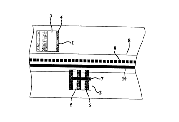
t=ig. 1 illustrates a document with an electrically conductive ink print 1 and
one OVD 2.
The specific combination of different safety elements results in an additional
coding.
This increases the test safety. This fig, illustrates the schematic set-up of
an electrically
conductive ink print 9 where alternatingly conductive strip-shaped zones 3 and
isolating
-~. strip-shaped zones 4 are arranged in parallel- The zones 3, 4 strip-shaped
in top view
run parallel to the document transport direction. The (~VD 2 consists of a
metal layer 5,
strip-shaped dematatlized zones 6 running parallel to the document transport
direction
as well as demetallized zone 7 running vertically to the document transport
direction.
Furthermore, fig. 1 illustrates the schematic view of the scanners 8 with a
number of
transmitting electrodes 9 and one receiving electrode 10.
Fig. 2 illustrates the block diagram of the test device according to this
invention,
consisting of one electronic control system, one capacitively woriting scanner
8 and
one electronic evaluation system. The electronic control system includes
mainly, in
- . addition tv the power supply, one demultiplexer 17, one oscillator 11 for
the supply of
energy for the transmitting electrodes and one oscillator 1x for the control
of the
demultiplexer,
The electronic evaluation system consists mainly of one power supply, one
arnpifier
13, one demodulator 14, one comparator 15, one microprocessor 16 with filter
as well
as filters for the suppression of interference and unwanted signals_
The transmitting and receiving electrodes are casted in a sensor carrier. They
form a
capacitivefy working scanner over the entire document front-feed width 8_ The
strip-
CA 02298494 2000-O1-24
1 6-
shaped receiving electrode runs transversely to the document front-feed
direction. The
transmitting electrodes run parallel to the receiving electrode. The distiance
between a
transmitting electrode and the receiving elECtrode is determined by the
document
typical electrically eonductuve test features_ By a side-by-side arrangement
of several
transmitting electrodes there is the possibility to detect several
electrically conductive
features in the longitudinal axis of the capacitively working scanner 8 at the
same time.
r
The resolution reached by this arrangement depends on the number of the
transmitting
electrodes used. In this design example the resolution is at a scannable point
per rnm
in lengthwise as well as transverse direction. The minimum distance between
adjacent
transmitting electrodes is IimitEd by the interfering capacitive coupling
among
themselves. In order to avoid this and in order to reduce interfering
influences of
adjacent transmitting electrodes the transmitting electrodes are controllEd by
a
multiplexer 17 one after another. 13y the arrangement of the transmitting
electrodes
over the entire document front~feed width the documents are tested in any
position.
That means it is not necessary to presort various documents in a document
handling
machine_
Fig. 3 illustrates the schematic view of the scanner 8 with a number of
transmitting
electrodes 9 and one receiving electrode 10. The contra! and evaluation is
carried out
according to the block diagram shown in fig. 2.
Fig. 4 illustrates the schematic view of a design of the capacitively working
scanner
with a transmitting Electrode 18 and a number of receiving electrodes 19. As a
modification of the block diagram according to fig. 2 the transmitting
electrode 18 is
controlled by means of the oscillator. The signals of the receiving electrodes
19 are
CA 02298494 2000-O1-24
-17-
processed by means of the multiplexer, The other part of electric evaluation
system
consisting of a power supply, an amplifier, a demodulator, a cornparator, a
microprocessor with memory as well as filters for the suppression of
interference and
unwanted signals is similar to the one in the block diagram according to
fig.2.
Fig. 5 illustrates the schematic view of another design of the capacitively
working
scanner with a number of transmitting electrodes 20 and a number of receiving
electrodes 21. They are altematingly arranged in one line. Accordingly, the
control
signals of the transmitting electrodes 20 as well as the evaluation signals of
the
receiving electrodes 21 are processed by means of multiplex and demultiplex
processes.
Fig. 6 to 8 illustrate the schematic view of scanners 33, 34, 35 and a
structured safety
feature 36. The structure of the safety feature 36 consists of a ring-shaped
safety
element 37, a strip-shaped safety element 38 and two rectangular safety
elements
39,40. The safety elements 37, 38, 39 Consist of electrically conductive ink
while safety
element 40 is optically similar to safety element 39 but has, however, no
electric
,..
conductivity. This increases the test safety since it is visually not
perceptible which
safety features are on a document. Simple manual devices include a scanner 33
according to fig. 6. The resolution is so low that only the strip-shaped
safety element 38
can be detected. Such manual devices are good for daily use because they can
be
manufactured simply, at low costs and for easy handling.
bevices with a higher resolution according to fig. 7 consist of a scanner 34
and allow,
besides the testing of a strip-shaped safety element 38, the testing of
additional safety
elements, in this case a ring-shaped safety element 37. The rectangular safety
elements 39, 40 are not tested. This is realised by a simple microprocessor
software
CA 02298494 2000-O1-24
-18-
~.,
which is only sensitive to certain safety elements. The rectangular safety
elements 39,
40 are not available in the memory as reference signals.
A higher resolution with a properly designed software for the microcontroller
is
illustrated in fig. 8. It allows the testing of all safety features, that is,
also the rectangular
safety elements 39, 40.
In order to meet the object speci>'led in this invention to contemplate a new
system of
the application of test features, test procedures and devices in order to
avoid that the
functioning of test procedures and devices is known or becomes quickly known
the
following use of test features, test zones and structures using a
corresponding
procedure application and including the devices according to this invention is
explained.
The following examples shall illustrate the application of this invention. For
a large
application of this invention it is necesary to fix groups of testing persons
who will
purposefully get a certain knowledge about a test system and who wilt carry
out the
counterfeit test and also the image detection and a condition test by means of
the
specified test method.
8y means of groups A, B and C the application of this test system shall be
explained.
Group A.
It is well-known that the state bank provides publications on active safety
features so
that the user can carry out a test himself according to instructions. These
publications
CA 02298494 2000-O1-24
- ~s-
refer to test methods which are carried out without aids and test methods
which are
carried out with aids. According to this invention the scanner sensor can be
mounted in
a manual device- By means of this manual device and a special software the
electric
conductivity can be tested.
The software is modified such that the scanner is activated by optical sensors
when the
bank note passes and then the pass length is measured. The electric
conductivity of
the ink print must be available in a defined value. By means of optical
sensors the end
of the bank note is determined and the scanner sensor is deactivated. Hence,
the
position of the electrically conductive test zone on the test object can be
determined.
By means of the controller the data are compared and evaluated with the stored
data.
Group B:
Group B has machines for the handling of bank notes. These machines are
equipped
with special sensors in order to detect different features. At the moment,
these
machines are equipped with sensors for the optical range andlor the detection
of
magnetic properties andlor the testing by means of a capacitive sensor for the
,:.--,
measuring of the pass length. By these capacitive sensors the presence of
electrically
conductive features larger than 6 mm can be detected. They don't allow a
detection of
several electrically conductive test zones in pass length. Besides, the
detection of a
different electric conductivity in the test xones is impossible. Structures
within a test
zone cannot be detected as well- By means of the specified scanner sensor
these tests
are possible so that this group B can cony out a higher-quality test. By means
of
special functional printing images and the device according to this invention
for testing
with a modfied software the machines can carry out this test.
CA 02298494 2000-O1-24
-20-
a--,
--
The software for group B is designed such that the scanner sensor is activated
by
means of optical sensors and afterwards the ring-shaped safety element 37 and
the
strip-shaped safety element 38 are read. The value of the conductivity is
fixed.
Deviations -~ 30°~ are rejected_
The scanner sensor is deactivated and evaluated by optical sensors_
group C:
The software is designed such that all test features are detected. By means of
optical
sensors the scanner sensor is activated. The pass length and pass width of the
structured safety feature 36, the ring-shaped safety element 37, the strip-
shaped safety
feature 38, the rectangular safety element 39 as well as the rectangular
safety feature
40 are detected as a non-conductive safety element. The electric conductivity
is given
and deviations larger or smaller than 309'6 are rejected.
In combination with other physical features the combined test increases the
safety
standard_
The specification of group C explained above shall be explained in detail as
follows:
Group C has a full software or hardware version , respectively, which has the
highest
quality and alt given structures and dimensions of the test field can be
detected.
As an additional coordination the rectangular test element 39 is designed as a
feature
print of different physical variables.
It is one possibility to design the rectangular test element 39 as a high-
quality
fluorescent feature. This means that this test element is activated by a light
source and
CA 02298494 2000-O1-24
z~ -
the time of persistence (remiscence) is determined after the light source went
out. An
optical sensor activates the test sensing system when the bank note passes.
The test
sensing system consists of an optical sensor and a scanner sensor for the
detection of
electrically conductive test fields. The optical sensor consists of a light
source and a
receiver. The test object is irradiated in a defined time. After this the time
of persistence
of the feature inks is measured at the receiver. This time of persistence is a
coding. 1n
,.-,
case of a present optical feature the capacitive scanner sensor is activated.
A single
test is also possible.
There is another possibility to design the rectangular test element 39 as a
fluorescent
feature with different ink emissions. That means that the feature print is
irradiated by a
light frequency a and tint a+ is emitted. For the light source with frequency
b tint b+
develops_ An optical sensor activates the test sensing system which consists
of an
optical sensor and the capacitive scanner sensor. The optical sensor consists
of two
light sources with different frequencies. By means of special filters it can
be achieved
that only one receiver is required. Another possibility is to use one light
source,
.,...,
however, two separate receivers with upstream filters_ The optical sensing
system
activates the capacitive scanner sensor if the optical feature is present. A
single test is
also possible in this case.
It is a third possibility to design the rectangular test element 39 as a
magnetic ink print.
An optical sensor activates the test sensing system when the bank note passes
which
consists of a magnetic reading head and the capacitive scanner. The magnetic
reading head can detect the presence or a coding. In case of a present
magnetic
feature the scanner sensor is activated_
CA 02298494 2000-O1-24
It is a fourth possibility to design the rectangular test element 39 with a
conductivity
50% lower than the ring-shaped safety element 3~' or the strip-shaped safety
element
38, respectively. For the detection a special test software is required which
only this
group has access to. In case the conductivity decreases further a static
measuring is
required for which a special single note test device is necessary.
Especially for the application in groups B and C the entire test system can be
varied
and especially for the testing of the Euro it can be nationally modified as
regards its
objects. Since the safety feature to be tested, such as in the Euro is the
same in all
states the test procedure as well as the test device, however, can be modified
and
changed at successive intervals in a different way in the various nations
depending on
the objects.
The application of the safety elements and test devices as specified above is
used as
follows: By means of the coded specific metallizations there can be an image
detection.
This image detection can be used for various purposes, especially sorting
purposes,
denomination and counterfeit detections. Another advantage of this test method
is the
,~~'.
condition control. l'he electric conductivity measuring allows to draw
conclusions to the
condition of the bank note paper. Highly worn paper minimizes the electric
conductivity
very much.
In this invention at hand the structure of safety elements and a device for
the test of
said elements was specified by means of precise design examples. However, one
should note that this invention is not limited to the details of the
spec~cation in the
CA 02298494 2000-O1-24
-23-
design examples since modifications and changes are claimed within the
framework of
the patent claims. The specific combination of diffraction-optically effective
safety
elements with other electrically conductive features results in another
ceding. At the
same time additional electrically conductive test features such as an
electrically
conductive safety thread can be classified by means of the test device
according to this
invention.