Note: Descriptions are shown in the official language in which they were submitted.
CA 02302014 2000-02-25
~, - , . .,
;,
.1 , ,, . , ,
. , ~ , -
. , ~ ~ , ,. ".
,~ > > _
v A ' 1 .
A read-only memory and read-only memory devices
The present invention concerns an electrically addressable non-volatile
read-only memory, comprising a plurality of memory cells which in a write
operation comprising a part of the manufacturing process of the read-only
memory, permanently each are assigned one of two or more logic states
according to a determined protocol which in the memory defines permanently
written or stored data, and a passive matrix of electrical conductors for the
addressing, wherein the passive electrical conductor matrix comprises a first
and
a second electrode structure in respective mutually spaced apart and parallel
planes and with parallel electrodes in each plane and provided such that the
electrodes form a substantially orthogonal x,y matrix wherein the electrodes
in
the first electrode structure comprise the columns of the matrix or x
electrodes
and the electrodes in the second electrode structure comprise the rows of the
matrix or y electrodes, wherein at least a portion of the volume between the
intersection of an x electrode and a y electrode defines a memory cell in the
read-only memory, wherein are provided at least one semiconductor material
with rectifying properties in relation to a selected electrical conducting
electrode material, and a first electrical isolating material, wherein the
semiconductor material in electrical contact with an electrode in the memory
cell forms a diode junction in the interface between semiconductor material
and
electrode material, and wherein a logic state in each case is given by the
impedance value of the memory cell, said impedance value substantially being
given by either the impedance characteristics of the semiconductor material or
the impedance characteristics of the isolating material, and the impedance
characteristic of the diode junction.
The invention also concerns a read-only memory device which comprises one or
more read-only memories according to the invention, and a read-only memory
device which comprises two or more read-only memories according to the
invention.
Matrix addressing of data storage locations or bit spots on a plane is a
simple
and efficient way of achieving a great number of accessible memory locations
with a moderate number of electrical addressing lines. In a square x,y matrix
with n lines respectively both in the x direction and the y direction the
number
of memory locations scales as n2. In one form or another this basic principle
is
at present implemented in a large number of different embodiments of solid
state memory means. In these the memory location comprises a simple
electronic circuits which communicates to the outside via the intersection in
the
matrix and a memory element, typically a charge storage device. Even if such
AMENDED SIaEET
CA 02302014 2000-02-25
-, , -.
., , ,
, ~ a >~ .
. . .. w o , ~ a ..
, ,
.." ,e as w
means have been technically and commercially very successful, they have a
number of disadvantages, and particularly each memory location has a complex
architecture which leads to increased costs and reduced data storage density.
In
the large subclass of so-called volatile memory means the circuits must
constantly sustain a current supply with accompanying heating and consumption
of electric power in order to maintain the stored information. On the other
hand
non-volatile means avoid this problem, but with the trade-off of a reduced
access and switching time as well as increased consumption and high
complexity.
Prior art provides a number of examples of semiconductor-based read-only
memories with electrical addressing in passive matrix. Thus US patent No.
4 099 260 (Lynes & al.) discloses a semiconductor-based read-only memory
(ROM) made as a large scale integrated device wherein self isolating bit line
surface areas of one conduction type are formed in a semiconductor substrate
and directly in a bulk area in the opposite conduction type. Channel stop
areas
of the same conduction type as the bulk area are formed in the intervals
between
the bit line areas. Metallic word lines which lie above and are orthogonal to
the
bit line areas, are formed separately from these by means of an isolating
layer.
The memory cell comprises a single Schottky diode. A diode of this kind will
be
formed or not at each intersection between a word line and a bit line
depending
on whether or not an opening is formed in the isolating layer during
manufacturing in order to permit the word line to contact a lightly doped
portion
of the bit line. A ROM of this kind is stated to have a small area, high
speed,
low power dissipation and low cost.
Further there are from US patent No. 4 000 713 (Bauge & Mollier) known a
device with semiconductor elements, such as Schottky diodes and transistors
integrated in the form of a matrix on chips. The matrix may be custom designed
in order to provide a desired function. For instance it may be used as AND or
OR matrices in programmable logic arrays (PLA) or as read-only memories
which are stated to have better properties with regard to storage density and
power dissipation. A first electrode structure with parallel metal electrodes
of
somewhat different design is provided on a semiconductor substrate of for
instance the p type. An oxide layer is provided on a semiconductor substrate
and
openings are formed in the oxide layer to provide anode contacts and cathode
contacts via metallic lines which constitute a first metal level in the
electrode
matrix. Two n+ areas are located under the cathode contacts. These areas
extend
to underlying collector layers such that a Schottky diode is formed. Above the
first metal level or electrode level an isolating layer is provided and over
this a
AMENDED SHE'
CA 02302014 2000-02-25
3 , ,_
' ~ ~ , . ":
' ,a s
" ' ' » w
second metal level which comprises for instance an orthogonal second electrode
structure. Openings through the isolating layer ensure contact with a cathode
contact in a group of such which are included in the separate element in the
matrix.
Finally there are from US patent no. 5 272 370 (French) known a thin-film
ROM device based on a matrix of open and closed memory cells formed in a
stack of thin films on glass or another substrate. Each closed memory cell
comprises a thin-film diode and it may by using stacks of semiconductor films,
for instance of hydrogenated amorphous silicon, wherein the separate films are
of different conduction types, be obtained diodes with different conduction
characteristics. Thereby the information content in the ROM matrix may be
increased. Each memory element which is formed with diode structure, may
then be set with different logic levels according to some manufacturing
protocol. Where the memory element does not have a diode structure or where
the semiconductors are covered by an isolating layer such that no electrode
contact is formed, the memory element may be used to form a determined first
logic level, for instance logical 0.
Even though the above-mentioned prior-art devices all realize electrical
addressing in passive matrix in an as per se known manner by providing diode
junctions in closed electrode contacts, they have partly due to using
different
types of semiconductors a relatively high degree of complexity. In the ROM
device as disclosed in the last-mentioned publication (US patent 5 272 370) it
may, however, be possible to store more than two logical values in the matrix,
but this presupposes use of different diode types and hence several layers of
differently doped semiconductors in the bit spot with diode junction.
The object of the present invention is hence primarily to provide a read-only
memory or ROM which permits electrical addressing in passive matrix to the
separate memory cell in the read-only memory and which does not need
refreshment in order to keep the data stored in the memory cell, while the
read-only memory shall be simply and cheaply realized using as per se known
technologies and methods as applied in the semiconductor and thin-film
technology.
Particularly it is the object of the present invention to provide a non-
volatile
read-only memory based on the use of organic materials, for instance polymer
materials, which realized in thin-film technology may be used both in
conductors, isolators and semiconductor materials, something which supposedly
AMENDED SHl~ET
CA 02302014 2000-02-25
_: .4 ., ~ ,..,
,, ,
- ; ,~, ".
v
.. .. " ..
shall provide more flexible technical solutions and especially a much reduced
cost than would be the case when using crystalline inorganic semiconductors.
Further it is also an object to provide a read-only memory which allows a
multilevel coding of predetermined memory cells or memory locations.
Finally it is the object of the present invention to provide a read-only
memory
which may be used to realize a volumetric read-only memory device.
These and other objects and advantages are achieved according to the invention
with a read-only memory which is characterized in that the y electrodes are
provided on a second electrical isolating material which is realized as strip-
like
structures of substantially same form and extension as the y electrodes and
provided adjacent to the x electrodes as part of the matrix, that the
semiconductor material is provided over the electrode structures, a contact
area
in the memory cell thus being defined by the portions which respectively
extend
along each side edge of the y electrode where it overlaps the x electrode in
the
memory cell, that a first logic state of a memory cell in the read-only memory
is
generated by an active portion of the semiconductor material covering the
whole
contact area of the memory cell, the diode junction thus comprising the whole
contact area of the memory cell, that a second logic state in a selected
memory
cell in the read-only memory is generated by both electrode structures in the
memory cell being covered by the first isolating material, that one or more
additional logic states in a memory cell in the read-only memory is generated
by
an active portion of the semiconductor material covering only a part of said
contact area, such that the data which are stored in the memory may be
represented by the logic states in a multi-valued code, and that said one or
more
additional logic states are given by impedance values determined by the
extension of the active portion of the semiconductor material, and the
extension
of the part of the contact area which forms the diode junction.
A first read-only memory device according to the invention is characterized in
that the read-only memory is provided on a substrate of semiconductor material
or between substrates of semiconductor material and via the substrates
connected with driver and control circuits for driving and addressing, said
driving and control circuits being integrated in the substrate or the
substrates
and realized in a semiconductor technology compatible with the substrate
material; and a second read-only memory device according to the invention is
characterized in that the read-only memory is stacked in horizontal layers in
order to provide a volumetric memory device, that the volumetric memory
device is provided on a substrate of semiconductor material or between
AMENDED SHEE'~
CA 02302014 2000-02-25
.~ ~ . .
-.
. .
' ' ~ a ~
" ' ' ~ , s w
substrates of semiconductor material and via the substrate or the substrates
connected with driver and control circuits for driving and addressing, said
driving and control circuits being integrated with the substrate or the
substrates
and realized in a semiconductor technology compatible with the substrate
5 material.
Wherein the read-only memory according to the invention constitutes a binary
logic memory, it is advantageous the first logic state which either represents
a
logical 0 or a logical l, is given by the effective forward bias resistance of
a
diode formed in a memory cell wherein the semiconductor material contacts
both the x electrode and the y electrode, and that the second or the
additional
logic states which correspondingly shall represent either a logical 1 or a
logical
0, is given by a selected resistance value for the first isolating material
provided
in a memory cell wherein the semiconductor material does not contact either
the
x electrode or the y electrode, said isolating material in a memory cell
preferably having an infinite resistance value.
Wherein the read-only memory according to the invention is realized as a
multilevel logic memory with one or more additional logic states, it is
advantageous that the first logic state is given by the effective forward bias
resistance of a diode formed in a memory cell wherein the semiconductor
material contacts both the x and y electrodes and that the additional logic
states
are given by determined resistance values for the isolating material provided
in
a memory cell wherein the semiconductor material at most contacts either the x
electrode or the y electrode and the selected determined resistance value in
each
case lies between the effective forward bias resistance of a memory cell
formed
in the diode, and infinite.
In a first embodiment of the read-only memory according to the invention the
first isolating material in selected memory cells is provided over the
electrode
structures in the form of a separate layer-like isolator patch which wholly or
partly covers the electrodes in the memory cell, a selected memory cell
dependent on the active portion of the semiconductor material and/or the diode
junction area in the latter case acquiring a logic state which corresponds to
a
level in a multi-valued code. Preferably the semiconductor material in this
embodiment may be provided over the electrode structures in a global layer and
besides over the isolator patch in the selected memory cells, or alternatively
be
provided over the electrode structures and adjacent to the isolator patch in
the
selected memory cells, such that semiconductor material and the isolator
patches
mutually flush in a common continuous layer.
AMENftED SHEET
CA 02302014 2000-02-25
-; 6 ., , '., , ,-..,
' ° o ~ p
~ ° ~ ,oe i~~
~ ~ ~
~ ° ~ ~ ~ ~
In a second embodiment of the read-only memory according to the invention the
first isolating material is provided over the electrode structures in the form
of a
substantially global layer, and with removed portions in selected memory
cells,
such that the removed portion wholly or partly exposes the electrodes in a
S selected memory cell, said memory cell dependent on the active portion of
the
semiconductor material and/or the diode junction area in the latter case
acquiring a logic state which corresponds to a level in a mufti-valued code.
Preferably the semiconductor material in this embodiment may be provided over
the electrode structures and over the isolating layer in a global layer and
besides
contact the electrode structures in the removed portions of the isolating
layer, or
alternatively be provided over electrode structures and adjacent to the
isolating
layer in the selected memory cells, such that the semiconductor material and
the
isolating layer mutually flush in a common continuous layer.
In a third embodiment of the read-only memory according to the invention the
semiconductor material in selected memory cells is provided over the electrode
structures in the form of a separate layer-like semiconductor patch which
wholly
or partly covers the electrodes in the cells, a selected memory cell dependent
on
the active portion of the semiconductor material and/or the diode junction
area
in the latter case acquiring a logic state which corresponds to a level in the
multivalued code. Preferably the first isolating material in this embodiment
may
be provided over the electrode structures in a global layer and besides over
the
semiconductor patches in the selected memory cells, or alternatively be
provided over the electrode structures and adjacent to the semiconductor patch
in the selected memory cells, such that the first isolating material and the
semiconductor patches mutually flush in a common continuous layer.
In a fourth embodiment of the read-only memory according to the invention the
semiconductor material is provided over the electrode structures in the form
of a
substantially global layer and with removed portions in selected memory cells,
such that the removed portions wholly or partly exposes the electrodes in a
selected memory cell, said memory cell dependent on the active portion of the
semiconductor material and/or the diode junction area in the latter case
acquiring a logic state which corresponds to a level in a multivalued code.
Preferably the first isolating material in this embodiment may be provided
over
the electrode structures and the semiconductor material in a global layer and
besides isolate the electrode structures in the removed portions of the
semiconductor layer, or alternatively be provided over the electrode
structures
and adjacent to the semiconductor layer in the selected memory cells, such
that
AMENDED SHEEt
CA 02302014 2000-02-25
- ~,
_ , ~
1 ~ . ; ~ a ..
~ "o ae~
o a
,, ~, ~s w
the first isolating material and the semiconductor layer mutually flush in a
common continuous layer.
Finally it is according to the invention advantageous that the semiconductor
material is amorphous silicon, polycrystalline silicon or an organic
S semiconductor, the organic semiconductor preferably being a conjugated
polymer.
According to the invention the semiconductor material may be an anisotropic
conductor. Preferably the semiconductor material may comprise more than one
semiconductor or possibly also be added or combined with an electrical
conducting material.
Preferably the semiconductor material, the isolating material and the
electrode
structures are realized as thin films.
The background of the invention and various examples of its embodiment shall
now be discussed in more detail in the following with the reference to the
accompanying drawing.
Fig. 1 shows schematically a general embodiment of a memory device with a
passive electrode matrix provided between backplanes or substrates,
fig. 2 schematic examples of sneak current loops which may arise in a matrix
of
this kind,
fig. 3a a first embodiment of a read-only memory according to the invention
and
seen respectively in plan view and section taken along the line A-A,
fig. 3b a section through the read-only memory in fig. 3a taken along the line
A-
A in a second variant of this embodiment,
fig. 4a a second embodiment of the read-only memory according to the
invention seen respectively in plan view and section taken along the line A-A,
fig. 4b a section through the read-only memory in fig. 4a taken along the line
A-
A in a second variant of this embodiment,
fig. Sa a third embodiment of a read-only memory according to the invention
respectively in plan view and section taken along line A-A,
fig. 5b a section to the read-only memory in fig. Sa taken along the line A-A
in
a second variant of this embodiment,
AMENDi:D SIiEEf
CA 02302014 2000-02-25
8 .,
~ a o
~ ' s , -~. snv
~ ~ f s
~ . , 9 7 v 1 ~
fig. 6a a fourth embodiment of a read-only memory according to the invention
seen respectively in plan view and section taken along the line A-A,
fig. 6b a section through the read-only memory in fig. 4a taken along the line
A-A in a second variant of the second embodiment,
fig. 7a an example of multilevel coding of a memory cell in the embodiment in
in fig. 3a,
fig. 7b an example of multilevel coding of a memory cell in the embodiment in
fig. 4a,
fig. 8a an example of multilevel coding of a memory cell in the embodiment in
fig. Sa,
fig. 8b an example of multilevel coding of a memory cell in the embodiment in
fig. 6a,
fig. 9 a section through a first read-only memory device according to the
invention, and
fig. 10 a section through a second read-only memory device according to the
invention.
The general background of the invention shall now be discussed more closely. A
generic matrix addressing system is shown in fig. l, wherein for instance m
electrical conducting lines 2 are mutually spaced apart and extend in a x
direction and with for instance n overlying electrical lines 4 which extend in
a y
direction and respectively form first and second electrode structures in an
orthogonal x,y electrode matrix. The x electrodes 2 and the y electrodes 4 are
provided sufficiently close to each other such that geometrically well-defined
overlapping areas or intersections between the electrodes are provided. The
volume near and between each intersection, coarsely defined by the overlapping
area which is given by the width of the intersecting x electrodes and the y
electrodes in these intersections, comprises what in the following will be
denoted as a memory cell 5, see fig. 2. The mutually overlapping areas of
respectively the x and the y electrodes 2;4, in a memory cell 5 will be
denoted
as the contact area of the memory cell. According to the invention data is
stored
in each memory cell as impedance values, for instance resistance values
between the x and the y electrode in each intersection. The logic state in
each
intersection or memory location is found by measuring electrical impedance
between the x electrode and the y electrode which intersect each other in the
memory cell.
~IMENDI:D SH~~'
CA 02302014 2000-02-25
." . . ' , ~ ,
» a
' -> ' i
~ ' ~ a 4 .i '.ws n~s
> i ,
f
,. ~ p w y y
Distinct from common known current-addressed and matrix-based memory
systems the present invention allows the use of a purely passive electrical
addressing, as there are no discrete active circuit elements in the memory
cells.
It is well-known that the use of electronic memories with memory cells in
passive matrix is encumbered with alternative current paths or sneak current
paths in the electrode matrix. This problem is indicated in fig. 2 where
alternative current paths generated by addressing the memory cell Sk, given by
the intersection between the electrodes mk, n, are indicated by thinner
stitched
lines to the neighbouring memory cells. When the size of the matrix, i.e. the
product x~y increases, then the sneak current problem also amplifies. If the
memory elements in each intersection has a purely resistive impedance this
implicates that the resistance difference in a write operation will be masked
by
currents which leak through alternative current paths, such as indicated in
fig. 2.
If the electrical connection in each intersection is given a highly non-linear
current-voltage characteristic, the sneak current problem may be reduced or
wholly eliminated. Quite simply this is achieved in a manner which is already
well-known and suggested in the art, namely by providing a rectifying diode in
series with the impedance or resistance in each intersection.
An essential goal of the present invention is forming a network of diodes of
this
kind in a manner which simple, cheap, reliable and which simultaneously allows
the use of suitable memory structures in the form of controllable impedances.
According to the present invention the x and the y electrodes may preferably
surround a layer of semiconducting material, for instance in thin-film
configuration. Particularly this semiconducting material may advantageously be
a conjugated polymer of the tiophene or PPV-type. By choosing a suitable
electrode material with regard to the semiconducting material, a diode
junction
is obtained at the electrode-semiconductor interface and the diode may be
given
very good rectifying properties. A simple linearized analysis shows that the
number of electrode intersections, i.e. memory cells which may be addressed
without distortion or noise due to sneak currents, is approximately equal to
the
diode rectification ratio in each intersection, i.e. the relation between
forward
and backwards flowing current at a given bias voltage.
Another basic problem with passive matrix memories as exemplified in fig. 1
wherein the continuous material layer with finite resistance extends in the
intervals between the intersections of the electrode matrix, is that currents
even
with perfect rectification in each intersection may flow between the electrode
lines 2, 4 in these intervals. Even if the path length in these intervals will
be
much longer than which is the case in the intersections, i.e. in the memory
cell,
AN1ENDE0 SHEff
CA 02302014 2000-02-25
1' 1 1 1 1 1 ~: t' 4 1 1 f 1
1 1 1
1 1 1, 1 1 1' 1 1 f 1 1
1 Y f
1 1. 1. 1. , 1 f ~' 1, p 1' 1. ~ t~ f f 1. 1.
1. 1. 1. 1. 1 1 1.
f Y
w w ~ t 1 1 1'. t- ~1 ~
rr 1-1.
and the layer between the electrode structures are extremely thin with high
surface resistance, the combined effect of many such current paths is
detrimental to the measured impedance and hence finally sets an upper limit to
the number of intersections and so also of memory cells which may be realized
in a passive matrix.
The last kind of crosstalk may be avoided by making the film conductance
highly anisotropic, i.e. with high conductance in the desired current
direction
and else low conductance. In case of fig. 1 this will correspond to high
conductance perpendicularly to the plane of the matrix and low conductance in
the matrix plane. Polymer compositions with properties of this kind have been
described in the literature, for instance in the paper "White light emission
from
a polymer blend light emitting diode" of M. Granstrom and O. Inganas, Applied
Physics Letters 68, 2:147-149 (1996), and electrode means and devices based
thereon have been disclosed in NO patent application No. 973390 which has
been assigned to the present applicant.
Starting with an as per se known basic structure as shown in fig. 1 wherein
the x
and y electrodes 2;4 are provided on each side of an anisotropic thin film
with
high rectification ratio in the intersections of the electrodes, data may be
coded
by a controlled deposition of an electrical isolating material between diodes
in
selected intersections, such this will be discussed in more detail in
connection
with fig. 3a. If such selected intersections are given an infinite resistance,
each
intersection or each memory cell can be binary coded, for instance with a
forward bias voltage which either gives logical 1 as R = RF, where RF is the
effective forwards bias resistance of the diode in this intersection, or logic
0 as
R = oo, where an infinite resistance on purpose have been inserted in the
. intersection. Higher data storage capacity will be obtained by using a
larger
range of resistance values, which is equivalent to several bits being stored
in
each memory cell, for instance with resistance values Rl, R2, R3,...,
RF<R1 <R2<R3<oo.
There shall now with reference to figs. 3-8 be described examples of
embodiments of the read-only memory according to the invention. In these
embodiments it is used a particular addressing geometry which simplifies the
adjustment tasks in the manufacture and offers a number of advantages. These
embodiments differ from those which are described in a parallel and on the
same date filed International application PCT/NO/9800263 with the same
priority base as the present application, in that the semiconductor material
and
the isolating material is not provided between the electrode structures in a
AMENDED SHEET
CA 02302014 2000-02-25
. 11 , ,
' - - ~,
~ . ,
. . . _ ,. ..
sandwich configuration, but instead provided over the electrode structures
which are arranged in a bridge configuration such as for instance evident from
fig. 3a and fig. 3b. Each of the y electrodes is here provided on strips 12 of
an
electrical isolating or dielectric material which substantially has the same
form
and extent as the y electrode 4 and rests on the x electrodes 2 provided
orthogonally to the y electrodes 4, such that there is no physical or
electrical
contact between the x and y electrodes 2;4.
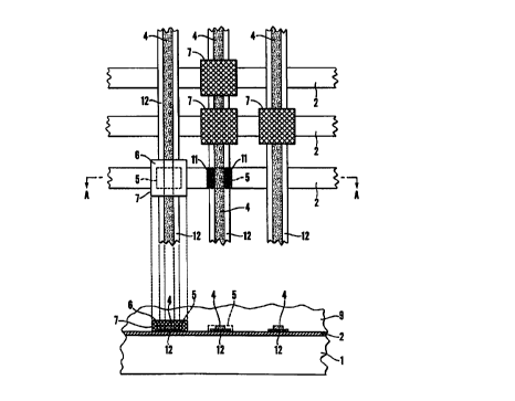
A first embodiment of the read-only memory according to the invention,
wherein the electrodes 2,4 are provided in bridge configuration, is shown
respectively in plan view and section in fig. 3a. Over the memory cells 5
which
is defined in the intersection between x and the y electrode 2;4 the data are
coded by the first isolating material 6 in selecting memory cells being
provided
over the electrode structures as a separate layer-like isolator patch 7. The
semiconductor material 9 is provided over the electrode structures with the
electrodes 2,4 and the isolator patches 7 and will only contact the electrodes
2,4
in a memory cell 5 where the isolator patch 7 is not present. The contact area
11
is indicated by a patching on the side edges on a y electrode 4 in a memory
cell
5 and the active area of the semiconductor material which in this case gives
its
impedance value, extends from the y electrode 4 through the semiconductor
material 9 to contact with the x electrode 2. Preferably the semiconductor
material which for the sake of clarity is deleted from the plan view in fig.
3a,
may be an anisotropic semiconducting material, but where for instance the
distance between the memory cells is not very small, i.e. the storage density
is
low, the semiconductor material may well be an anisotropic conducting
semiconductor material. In a variant of the embodiment in fig. 3a the
semiconductor material 9 is provided over the exposed electrodes 2,4, and
adjacent to the isolator patches 7, such that the surface of the isolator
patches 7
and the semiconductor material 9 mutually flush, as this is shown in fig. 3b.
Thereby the distance between the substrates 1,3 may be reduced and there is
nothing against the electrode 4 resting against substrate 3 which, of course,
is
electrically isolating.
It will also be possible to employ a multilevel coding in the input of data
which
are to be stored in the read-only memory of the embodiment as shown in fig.
3a,
and this will be described in greater detail below in connection with fig. 7a.
A second embodiment of the read-only memory according to the invention is
shown in fig. 4a. Here the memory cells instead are coded by isolator patches
7
using a substantially global layer of an electrical isolating material 6 which
is
provided over the electrode structures, but with removed portions 8 in
selected
AMENDED SHEET
CA 02302014 2000-02-25
' ., s , '' " ,, ,,
~12 > > ° '
o , , a , o ;,
~ ~ a ~ .".s a~a
o -
, ~ , a
"~, ~e as w
memory cells S. A global semiconductor layer 9 is provided over the isolating
layer 6 and will only contact the electrodes 2, 4 in the memory cells 5 at the
removed portions 8 of the isolating layer 6. The contact areas 11 are formed
in a
corresponding manner as in the embodiment in fig. 3a. Also in the plan view in
fig. 4a, is the semiconductor layer 9 for the sake of clarity deleted. The
semiconductor material 9 may also in the embodiment in fig. 4a be provided
only in the removed portions 8 such that its surface are flush with the
surface of
the isolating layer 6 as shown in fig. 4b. The removed portions 8 will then
form
isolated memory cells 5, and the semiconductor material in these memory cells
hence need not be an anisotropic semiconducting material, but may just as well
have isotropic conducting properties, as the semiconductor material does not
form a continuous layer where blind currents or bulk currents may pass between
the memory cells. Also here the y electrodes 4 may besides rest against an
electrical isolating substrate 3. The surface of the y electrodes will then,
of
course, also be flush with the surfaces of the semiconductor material and the
first isolating material. In the embodiment shown in fig. 4 it is further
possible
to implement a multilevel coding, such this shall be discussed in greater
detail
below in connection with fig. 7b.
A third embodiment of the read-only memory according to the invention
isshown in fig. Sa. It differs from the two previous embodiments in that by
the
semiconductor material 9 being provided in the form of semiconductor patches
10 in selected memory cells 5, and coding for instance the first logical
value,
while the first isolating material 6 is provided over the semiconductor
patches
10 and the open memory cells 5 in a substantially global layer. Also in the
plan
view in fig. Sa this layer is for the sake of clarity deleted. The
semiconductor
patches 10 are mutually isolated by the isolating material 6 and may hence be
anisotropic conducting semiconductor material, as blind currents or bulk
currents between the memory cells 5 will not be present. The contact areas 11
define as before the active portion of the semiconductor patch, said active
portion of course extending from the side edges of the y electrode and to
contact
with the underlying x electrode in the memory cell. Also in the embodiment in
fig. Sa the isolating material may be provided such that it is flush with the
surface of the semiconductor patches 10 as shown in fig. Sb, and the y
electrodes 4 are resting against the substrate 3. Functionally and
geometrically
the embodiment in fig. Sb does not differ from that in fig. 4b, but in the
embodiment in fig. 4b the isolating layer 6 with the removed portions 8 is
first
deposited, while the semiconductor material 9 thereafter is deposited in the
removed portions 8, for instance by first being provided as a global layer
both
over the isolating layer 6 and the removed portions 8 and thereafter scraped
off
AMENDED SHEET'
CA 02302014 2000-02-25
,,
'. 'i
'' 13 " a _ , . '..
s , ~ a
s ~ " ,~ _-!
"', , ',~~ ' s
r 3 ~ !
such that it only will be present in the removed portions 8. In the variant
embodiment in fig. Sb the semiconductor material 9, however, first is
deposited
as semiconductor patches 10 and thereafter the isolating layer 6 is deposited
substantially globally over the semiconductor patches 10 and the remaining
open memory cells, whereafter it is scraped off until it is flush with a
semiconductor patches 10 as shown in fig. Sb.
Also in the embodiment in fig. Sa a multilevel coding may be used, such as
will
be discussed in greater detail below in connection with fig 8a.
A fourth embodiment of the read-only memory according to the invention is
shown in fig. 6a. Here the semiconductor material 9 is deposited over the
electrode structures as a substantially global layer but with removed portions
or
windows 17 in selected memory cells 5 such that a first logic state in binary
coding is only obtained in the memory cells wherein the semiconductor material
9 is provided and the contact areas 11 are present, while another logic state
is
obtained in the memory cells which are located in a removed portion of the
semiconductor material. Over the semiconductor material a first isolating
material 6 is now deposited in a substantially global layer which for the sake
of
clarity, however, is deleted from the plan view in fig. 6a. Also here the
isolating
material may be deposited only in the removed portions 17 in the semiconductor
material such that the surface of the isolating material 6 is flush with the
surface
of the semiconductor layer 9, as shown in fig. 6b, while the y electrodes 4
simultaneously may well rest against the isolating substrate 3. It will easily
be
seen that the embodiment in fig. 6b is geometrically and functionally analogue
to that in fig. 3b, as i't is only the sequence of the arrangement of
respectively
the semiconductor material 9 and the isolating material 6 which differs.
Also in the embodiment in fig. 6a it is possible to employ a multilevel coding
as
this will be described in greater detail in connection with fig. 8b.
The embodiments in fig. 3-6 allow, as mentioned, a multilevel coding of data
in
preselected memory cells. In this case it is presupposed that a semiconductor
material with anisotropic electrical conducting property is used, for instance
in
the form of a conjugated polymer. The semiconductor material will then contact
respectively the x electrode and the y electrode in the contact areas 11 which
respectively are located along the side edges of the y electrode where it
intersects the x electrode. Each memory cells will hence comprise two contact
areas and have active portions which extend through the semiconductor material
and between the y electrode along each side edge thereof and to the x
electrode
over at least a part Ow of the width w of the x electrode. A multilevel coding
of
AMENDED SKEET
CA 02302014 2000-02-25
a ;o - ,
. , 14.: ,, _ . , ,
7 ,. , ~ ~ , ~ n s
~~,~~,s oev
v
~~ w w
data which are stored in a memory cell will now take place by adjusting the
length of the contact area, such that the impedance value of the memory cell
in
question arrives between a maximum value, for instance infinite, and a value
dependent of the diode forward bias voltage.
In practice this may be done by using an isolator patch 7 in the memory cell
such that only a part of the x and the y electrodes 2;4 at the intersection of
the
electrodes in the memory cell is covered. Thereby a contact area is exposed to
the not shown semiconductor material 9, such as is apparent from fig. 7a which
corresponds to the embodiment in fig. 3a, but with multilevel coding of
preselected memory cells. Fig. 7b corresponds to the embodiment in fig. 4a and
differs from the embodiment in fig. 7a in that the isolating material 6 is not
provided in the form of patches 7, but as a global layer with removed portions
or windows 8, wherein the not shown semiconductor material is provided and
contacts the x and y electrodes 2;4 in the memory cell at the contact areas 11
which are located under the semiconductor material and along the side edges of
the y electrode 4, such that the active portion of the semiconductor material
contacts the electrodes 2,4 over a contact area with a width 0w which is
smaller
than the width w of the x electrode.
If the semiconductor material once more is provided over the memory cell in
the
form of a semiconductor patch, contact areas 11 as shown in fig. 8a are
obtained
with a width 4w which only comprises a part of the width w of the x electrode
2. The active portion of the semiconductor 9 extends between the electrodes
2,4
in the contact areas 11. This embodiment corresponds to that in fig. Sa. In
the
same manner it may in the semiconductor material 9 in fig. 8b, which
corresponds to the embodiment in fig. 6a, be provided a removed portion or
window 17 such that there once more are obtained contact areas 11 with a width
Ow which is less than the width w of the x electrode.
By now adjusting the geometrical form of respectively isolator patches 7,
semiconductor patches 10 or the removed portions 8;17 in the isolating
material
6 respectively the semiconductor material 9, the coding of data in a memory
cell
may take place in several levels.
It shall be understood that the patches 7,10 and the removed portions 8,17 may
have a form which differs from that shown respectively in fig. 7a,b and 8a,b.
It
is for instance possible to pattern patches and removed portions such that
they
obtain the form of stripes respectively slots, but still are designed such
that the
contact areas 11 which provide the desired levels in a multivalued logical
code,
are obtained.
AMENDED SHEET
CA 02302014 2000-02-25
:,
., 77 ~ ~ - '1
7 ~ 7 '~ '7 1 , 1
'7 ) , ~ ~ ~ ~ ) ~ ~ 3 ~ 1
7
7 '1 , 7 ~ ~ ~ ~ ~ ~ ~
That the semiconductor material is provided over the electrode structures has
a
number of significant advantages. For the first electrode matrix and both the
first isolating material 6 and the isolator strips 12 may be deposited by
methods
and equipment well-known in semiconductor technology, before the
semiconductor layer is applied globally. Thus a number of adjustments may be
performed with high precision in a sequence layer after layer over the same
substrate and critical steps in the adjustment avoided, as it is not necessary
to
join the substrates 1 and 3 together in a sandwich configuration with high
mutual positioning accuracy. For the second may the substrates with
respectively the x electrodes and y electrodes 2;4 may be manufactured as
semiproducts, i.e. without the isolating material 6 and the semiconductor
material 9. Such semifinished blanks may be stored awaiting data coding and
final processing. In the embodiment in fig. 6 the substrates may for instance
be
fabricated in crystalline silicon. As known from NO patent application 973782,
which is assigned to the present applicant, a monolithic structure may be
chosen
where active circuits which provide interconnections, logical functions,
signal
routing, amplification etc. may be built into the silicon substrate and
connected
directly with the x and y electrodes on the same substrate. The whole
construction apart from the uppermost semiconductor layer, may be completed
in succeeding process steps which without difficulty may implemented by
standard technologies for processing of semiconductors. The uppermost
semiconductor layer is applied globally. The semiconductor material used must
have suitable rectifying and conducting properties, while it is desirable with
low
bulk costs, simple processing, long lifetime etc. and must be such that
optimal
contact with the electrode structures is obtained. As semiconductor material
may for instance conjugated polymers either of the PPV or tiophene type be
suitable. Alternatively amorphous silicon or polycrystalline silicon may be
used.
A particularly simple and cheap solution is obtained when the semiconductor
material is conjugated polymer which may be applied by doctor blading or by
spin coating, dip coating or meniscus coating.
It shall here be remarked that coding of data with the use of mufti-valued
code
places greater demand on discrimination when reading the impedance value in a
memory cell, and if there is a present danger of bulk and sneak currents
masking
the impedance value signal, either the mutual distance between the electrodes
2,4 in each electrode structure and hence the memory cells 5 may be increased
or else the mufti-valued code may be employed with the embodiment variants
shown in respectively fig. 4b and fig. Sb, which easily will allow the memory
cells to be located with a greater area density and with maintenance of the
discrimination necessary to obtain a readout of data stored for instance in a
AMENDED SKEET
CA 02302014 2000-02-25
. ~ 16 - ; v ..-'~, ., y,
n s n s
' ' ~ ~ ~ 'oo~ oov
~ s
". . ~ s~ w
two-bit code, i.e. with two levels between the code level given by
respectively a
complete masking of the contact area in the memory cell and a complete
exposure of the contact area in the memory cell. It is, however, supposed that
it
will be possible to increase the number of levels in the code, for instance
using
three- or four-bit coding. The latter is represented by sixteen levels and
hence
the realization will be a question of dimensions and attainable pitch if the
manufacture of the memory cells takes place with conventional
micro-photolithographic methods.
It may be expedient to form the semiconductor material from several
semiconductors, for instance provided in layers, such as known in the art, in
order to obtain special types of diodes, such as also known in the art, or in
order
to vary the impedance characteristics. For the same purpose also the
semiconductor material may be combined with or added an electrical conducting
material.
One or more read-only memories ROM according to the invention may
advantageously be provided on a semiconductor substrate 1 of for instance
silicon. In this substrate or integrated therewith in a compatible
semiconductor
technology there may be provided driver and control circuits 13 for the
read-only memory. An embodiment with four read-only memories ROM
provided for instance on a silicon substrate 1 with integrated driver and
control
circuits 13 is shown in fig. 9.
Instead of providing the read-only memories in a planar configuration, they
may
also be stacked vertically in layers, such as is shown in fig. 10. Once again
the
semiconductor substrate 1 of for instance silicon integrated with driver and
control circuits 13, is used. Along the side edges of a stacked memory device
of
this kind there may be provided addressing and driver buses 14 and in order to
connect the electrodes in the respective electrode structure, i.e. the
electrode
matrix, to the driver and control circuits in silicon substrates as this is
indicated
in fig. 7 which shows an embodiment with stacked read-only memories ROM
15,...15" which mutually are isolated by isolating layers 161...16, for
instance
ceramic.
Read-only memories and read-only memory devices according to the invention
could advantageously be realized in card format compatible with standard
interfaces as commonly used with personal computers. In practice the read-only
memory realized in a read-only memory device may be implemented in known
thin-film technology and the read-only memory device will integrated with the
silicon substrate appear as hybrid device. In practice it has turned out that
A~E~~~~ sir'
CA 02302014 2000-02-25
._ . _ _
~S . ~' ,~ _ . . 7
1 1 Z 1
.~ l
1 ~ 1
. . . _.1 7~ 1a
read-only memories according to the invention may be made with a thickness of
electrode structures and memory cells of at most a few micrometers and with
realistically at least two memory cells per p,m2 with the use of present
technology. A read-only memory with one storage layer and an area of 1 cm2
S will hence store 25 Mbyte with binary coding. By using two- or four-bit
coding,
something which seems realistic, the data storage density may, of course, be
correspondingly increased. It is assumed that it also will be realistic to
reduce
the size of the memory cells further such that a quadrupling of the storage
density in this way may be achieved. It will hence be possible to store some
hundred Mbytes in each read-only memory and the data storage density will, of
course, increase proportionally with the number of stacked layers in a read-
only
memory device configured volumetrically.
Implemented with standard card interfaces for use in personal computers or in
decoder devices for play-back equipment for reproducing sound and picture
material it will hence be possible to employ the read-only memory according to
the invention as data carrier for source material which else usually is stored
on
media such as CD-ROM.
Writing to the read-only memory according to the invention, i.e. input and
coding of data, is implemented in and integrated with manufacturing processes.
Preferably the read-only memory is manufactured with the use of well-known
thin-film technologies and photolithographic methods. Basically all materials
may be provided in global layers and electrode structures and patches and
removed portions (windows) formed with the use of photomasks and etching.
"Writing" of data then takes place by "coding" photomasks for patches or
windows with positioning and dimensioning the patches or windows of the mask
in accordance with a determined protocol, such that each memory cell is
correctly coded. Processes of this kind may easily be implemented for
manufacturing of large series of read-only memories with the same source
information, for instance program material for music or films.
AMENDED SH~~i'