Note: Descriptions are shown in the official language in which they were submitted.
CA 02303613 2000-03-31
SPECTROMETER
Field of the Invention
The invention relates to a spectrometer.
Backsround of the Invention
The trend in modern spectrometer systems is towards compact and economical
detectors affording fast measuring times and a moderate spectral resolution of
5 to 20 nm.
Typical applications for such sensors are in the areas of colour measuring
techniques or
industrial process control.
Spectrometers based on the known principle of diode arrays have the potential
to fulfill the above mentioned requirements and form the basis for the present
invention.
The conditions for the applicability of the invention are discussed below.
The diode array affords a parallel assessment of the entire measured spectrum
leading to fast measuring times.
The required spectral resolution is realized with a compact spectrometer
geometry with a focal length of less than 30 mm. Several examples are
demonstrated with
classical spectrometer arrangements based on planar gratings, e.g. a
demultiplexer of the
Ebert-Fastie geometry as described in US Patent No. 4,744,618, or concave
gratings with
an aberration correction, e.g. EP-A 0 489 286.
An economical production requires the use of modern production and
assembly techniques. The cost for such spectrometers is mainly determined by
three
factors: the cost of the components of the diode array and the diffraction
grating as well as
the cost for the fine tuning of the optical system.
Diode arrays are offered commercially by several manufacturers either in a
ceramic or in a plastic housing, for example by Hamamatsu. This type of
detector
manufacture is used in existing diode array spectrometers, e.g. EP-A 0 489
286.
Nevertheless, this detector geometry has several fundamental disadvantages.
First, a quality housing made from ceramic is very expensive and contributes
largely to the total cost of a detector unit. Second, for the present
application the position
of the light sensitive detector area is not sufficiently specified relative to
the outer
dimension of a standard housing, particularly in a vertical direction. For
this reason, the
housing cannot serve as a mechanical reference during assembly. The diode
array inside
the housing, i.e. the actual detector chip or the diffraction grating, has to
be actively
1
CA 02303613 2000-03-31
positioned during assembly on the spectrometer (U.S. Patent No. 5,040,889, EP-
A 0 727
681, EP-A 0 489 286). This manufacturing procedure is costly and associated
with high
additional costs.
Classical gratings are replicated in an epoxy layer on an optical glass
substrate.
The procedure is demanding and is not suited for an economical production in
large
quantities. The costs for the grating can be dramatically reduced by using
plastic gratings
that are produced in an injection moulding process. This technology has
recently become
available. The injection moulding process allows for the direct fastening of
very precise
mechanical positioning aids on the grating component affording a simple
assembly of the
grating at the central spectrometer module without active adjustment.
The main problem with the use of plastic gratings is however their great
temperature sensitivity. The lines of the grating expand proportionally with
the thermal
expansion coefficient of the plastic material which causes a shift of the
measured spectrum
with respect to the diode line and introduces an error in the calibration of
the wavelength
of the spectrometer. Since optical injection moulded plastic materials have
thermal
expansion coefficients in the order of magnitude of 8x10⁻⁵/ K, approximately
10 times
larger than glass, this spectral shift becomes the main component in the
temperature drift
of the spectrometer. Thus, a compensation for the temperature drift is a
prerequisite for
the application of this technology.
Existing techniques for the compensation of temperature drifts of diode array
spectrometers are disclosed in documents EP-A 0727 681 and US Patent No.
4,709,989.
The techniques are based on the use of materials having a low thermal
expansion
coefficient and an exact adaptation of the thermal expansion coefficient of
the various
spectrometer components. US Patent No. 4,709,989 relates to the adaptation of
the
thermal expansion coefficient of the spectral module to the materials of the
imaging optics
through the use of a ceramic material. EP-A 727 681 discloses an adaptation of
the
expansion coefficient of the spectral module made of ceramics to the diode
array made of
silica. Both techniques attempt to yield an approximately even thermal
expansion of the
entire spectrometer such that the angles of the optical path inside the
spectrometer remain
the same and the thermal drift is minimized. However, both techniques are
restricted in the
choice of material for the spectral module and hence can not be used for
economically
producing spectral sensors from plastic materials.
Thus, there is a need to overcome this difficulty and to improve a
spectrometer
such that it is very easily and economically assembled, e.g. from components
made of
2
CA 02303613 2000-03-31
plastic materials, to yield, even with the use of plastic components, a small
thermal drift
sufficient for practical applications.
A spectrometer of the prior art is described in US Patent No. 5,040,889. In
this prior art spectrometer, the detector is arranged on a base board which is
moveable
relative to the spectrometer housing (carrier) and adjustable by means of a
micrometer
screw. After successful adjustment, the base board is glued in place. The
manufacture of
this spectrometer is relatively construction intensive and labour intensive
and hence
requires great additional costs. Further, the temperature is continuously
measured in these
prior art spectrometers and an automatic re-calibration is carried out at
predetermined
temperature changes and at certain time intervals. Hence, only the temperature
profile of
the sensitivities of the single cells of the detector and their signal
amplifiers can be
compensated for but not the temperature dependent shift of the measured
spectrum with
respect to the diode array and thus the resulting error in the wavelength
calibration of the
spectrometer. The last mentioned problem is not discussed whatsoever in US
Patent No.
5,040,889.
Summary of the Invention
The solution of the object underlying this invention is discussed in the
characterizing portion of the independent claim. Preferred embodiments in
accordance
with the present invention are the subject of the dependent claims.
The new spectrometer geometry in accordance with the spectrometer of the
present invention does not require a housing for the detector, particularly
the diode array,
and is economically produced. Further, the particvlar spectrometer geometry
allows a
simple installation at the carrier.
Independently therefrom, mounting the detector on a base board in accordance
with the present invention, especially in combination with an adaptation of
the choice of
material for the carrier, the diffraction grating, ^a.nd the base board with
respect to their
expansion coefficients, allows for a complete compensation of the temperature
drift in
spectrometer systems having components made from plastic materials. The
compensation
in accordance with the present invention is based on an optimum geometric
arrangement
and connection of the carrier and the detector. This new technique provides a
free choice
of material and allows for the consideration of additional technical
parameters of the
production, such as the manufacturing costs.
3
CA 02303613 2000-03-31
In accordance with the invention, the base board is mounted to a carrier in
such a way that a temperature dependent shift of a measured spectrum with
respect to a
detector is at least approximately compensated for, the temperature dependent
shift being
caused by a thermal expansion of the base board.
Brief Description of the Drawin2s
Exemplary embodiments of the present invention are further described by way
of the following drawings in which:
Fig. 1 shows a sectional view of a preferred embodiment of a spectrometer in
accordance with the present invention;
Fig. 2 shows a base board of the spectrometer presented in Fig.1 provided with
a
diode array;
Fig. 3 shows a view of the carrier of the spectrometer with a lifted off and
unmounted base board; and
Fig. 4 shows a sketch explaining the determination of the temperature drift.
Detailed Descriotion of the Invention
A diode array spectrometer in accordance with the present invention is
generally constructed from several base components: a carrier I with a
possibility for
mounting a light input 2, such as an optical fiber and/or mechanical entry
gap, a detector
in form of a diode array 3, optical components for imaging the incoming light
onto the
diode array 3, and a diffraction grating 4 for dispersing the measurement
light that was
provided through a light input into its spectral components.
Fig. 1 shows a preferred embodiment of the invention, with respect to
geometry, based on a concave reflexion diffraction grating having correction
for imaging
errors. In this arrangement, the concave reflexion diffraction grating 4
provides optical
imaging of the incoming light and a spectral dispersion of the measurement
light.
Up to this point, the described spectrometer is substantially in agreement
with
the state of the art as was described above in conjunction with the cited
prior art
references.
Fig. 1 depicts the carrier as a hollow carrier produced with very precise
outer
dimensions. The carrier has the form of a cylindrical hollow body for an
optimum
temperature response and is advantageously made from a plastic material using
an
injection moulding procedure. Mechanical positioning and mounting aids for
additional
4
CA 02303613 2000-03-31
components are installed at the carrier 1, analogously to EP-A 0 194 613. The
concave
reflexion diffraction grating 4 is preferably made from a plastic material
using an injection
moulding procedure or by means of other replicating techniques. The optically
active area
of the concave diffraction grating has a highly reflective layer within the
spectral region of
the measurement (for ex., for visible light aluminum is used with a protective
layer of
quartz (Si02)). Mechanical positioning aids are formed on the grating
component made
from a plastic material for allowing a precise mounting on the carrier 1 and
an accurate
orientation of the grating lines. The mounting of the grating onto the carrier
1 is carried
out by means of a supporting board 5.
The light input is formed by a sliding tube 6 having an optical fibre 7 and a
mechanical entry gap 8. Alternatively, the optical fibre itself forms the
mechanical entry
gap. The sliding tube 6 is positioned in a guiding bore on the carrier, is
oriented by means
of a mechanical guide track, and is positioned across from a reference
position on the
carrier.
Starting with Fig. 1 the invention and particularly its differences from the
prior
art are further explained below. The method in accordance with the present
invention for
the support and mounting of a diode array as well as the compensation for a
temperature
drift is not only applicable to geometries according to Fig. 1 but is also
directly applicable
to other spectrometer geometries, such as the Czerny-Turner, Ebert-Fastie, or
Littrow
arrangements, which are also based upon even gratings.
Measurement light coming from the entrance 2 is imaged onto an exit area by
the reflexion diffraction grating 4 where it is dispersed into its spectral
components. The
centre of the light input and the normal 9 through the centre point of the
grating define a
plane, the so-called dispersion plane, in which the spectral dispersion of the
measurement
light takes place. The grating lines of the reflexion diffraction grating 4
are then oriented
in the centre point of the grating perpendicular to the dispersion plane, in
this example
perpendicular to the plane of the drawing. -
The diode array 3 needs exact positioning in the exit area across the spectrum
of the measurement light. Typical demands upon the precision of the
positioning of the
diode array are +/- 0.1 mm within the exit area and less than +/- 0.050mm in
the depth of
field perpendicular to the exit plane. This precision is not achieved with
commercial diode
arrays in standard housings.
The present invention provides a new possibility for mounting diode arrays 3
or other detector types onto the carrier 1 of the spectrometer. The
geometrical arrangement
5
CA 02303613 2000-03-31
in accordance with an embodiment of the present invention is depicted in Fig.
2. In
accordance with one embodiment of the present invention, a detector chip 10
(diode array
field) made from a semi-conductor material is glued directly to a planar base
board 11,
without the typical housing. Preferably, the base board is a conductor board
("Printed
Circuit Board"(PCB)), which allows for a direct equipment with an additional
electronic
circuit. Alternatively, the base board is made from other materials, e.g.
ceramics.
In addition, a protective frame 12 can be mounted on the base board 11 around
the detector chip 10. This frame 12 is preferably higher than the detector
chip 10 in order
to protect electrical contact wires ("bonding wires") on the detector chip
during
manipulation and mounting of the detector chip.
The electrical wires can be guided from the base board 11 to a main wire
board, not shown, via a flexible cable 13.
In accordance with an embodiment of the present invention the surface of the
base board can serve as a mechanical reference for the vertical positioning of
the detector
chip 10 relative to the surface of the base board 11, since the thickness of
the detector chip
10, which is made from a semiconductor material (generally silica for visible
light), is
precisely defined through a manufacturing process of integrated electronic
circuits
(generally better than +/- 0.01 mm).
In the text below the terms diode array and detector chip are used
synonymously where there is no danger of mistaking one for the other.
Two rectangular ribs 14 are formed on the carrier 1 of the spectral module for
the vertical positioning of the diode array 3 perpendicular to the base board
11. The
rectangular ribs 14 are arranged below and above a longitudinal axis 15 of the
diode array
and form a component for maintaining a distance to the base board 11. Fig. 3
depicts the
structure of the carrier in detail. Between the ribs 14 is a rectangular
opening 16 that
serves as an aperture for the measurement light.
When glued, the detector chip 10 is laterally positioned in the plane of the
base
board 11 across from the reference points on the base board. The positioning
and glueing
can be carried out automatically and economically with the required precision
by means of
a tipping machine as used in the production of semiconductors. Reference
points can be
determined in several ways, for example from across the outer edges of the
base board.
Preferably, the reference is made by means of mechanical positioning aids on
the base
board 11, which allow a simple mounting on the carrier of the spectral module.
6
CA 02303613 2000-03-31
The spatial distribution of the measured spectrum is fitted to the light
sensitive
area of the diode array in diode array spectrometers and thus consists of a
rectangular area
with a height in the order of magnitude of lmm and a length of several
millimetres, which
are chosen to be slightly smaller than the length of the diode array. Hence,
an absolute
shift of the measured spectrum in the direction of the longitudinal axis of
the diode array is
not critical as this shift can be taken into consideration when calibrating
the wavelength.
However, a tilt of the measured spectrum with respect to the diode array is
particularly
critical for the mounting. In this case, an overlap between the diode array
and the
measured spectrum is not guaranteed anymore for the entire spectrum, which
causes a
significant signal loss.
For this reason, the mechanical positioning aids in Fig. 2 are preferably in
the
form of a round hole 17 and an oblong hole 18 in the base board 11. The centre
of the
round hole 17 can serve as an absolute reference position. The oblong hole 18
needs to be
arranged such that a tilt with respect to the longitudinal axis of the diode
array is
prevented. In order to achieve an optimum thermal stability in the assembled
state with
the carrier 1 of the spectrometer, both of the positioning holes 17 and 18
have to be
arranged on the same side of the diode array 3 and close to the reference axis
9 of the
carrier 1. Preferably, the glueing of the base board 11 and the carrier 1 is
carried out at the
positioning holes 17 and 18. The exact position of the positioning holes 17
and 18 on the
base board 11 with respect to the detector chip 10 is used as a free parameter
for the
compensation of the temperature drift. The compensation method and the
calculation of
the optimum position of the positioning holes is described below.
Corresponding positioning structures are mounted to the carrier. In the
preferred embodiment with the circular hole and the oblong hole in the base
board 11, two
mechanically close-fitting cylindrical rods 19 are used, as shown in Fig. 3,
onto which
base board is placed.
During the mounting, the base board 11 is placed on the positioning structures
19 on the carrier 1. The bearing surface on the carrier is defined through the
ribs 14. A
firm mechanical connection between the two parts is achieved by glueing at the
positioning structures: round hole, oblong hole, and positioning rods. In
addition to the
firmly glued area the base board can be pressed onto the bearing surface of
the carrier with
a spring in order to increase the stability.
7
CA 02303613 2000-03-31
As a last step in the assembly, the detector unit, i.e. base board 11 with
mounted diode array3, and the carrier 1 are preferably insulated with black
paint in order
to isolate external scattered light.
It is necessary to distinguish between two basically different components for
the compensation of the temperature drift: first, a change in the signal
strength and second,
a spectral shift of the measured signal with respect to the diode array. The
first drift
component, the change of the signal strength, is not critical for most
applications. This
drift is completely compensated by carrying out measurements on a reference
channel or
with a white reference sample.
However, a wavelength dependent shift of the measured signal on the diode
array is an interfering factor. This shift corresponds to another wavelength
calibration of
the spectrometer and can not be compensated by a simple reference measurement.
Thus, the invention is mainly concerned with the compensation of the
temperature drift to minimize the spectral drift in the dispersion plane.
Consequently the
spectrometer unit needs to be constructed such that light of a certain
wavelength always
hits the diode array at a same position independently of the temperature. If
this condition
is met, a constant signal intensity is usually achieved.
Contrary to the prior art, the compensation technique in accordance with the
present invention is based on a geometrical optimization and not on a choice
of materials
having substantially similar thermal expansion coefficients. The position of
the
mechanical fastening of carrier and base board and the exactly defined
position of the
detector thereon serve as a free optimization parameter. This yields a greater
degree of
freedom than choosing the materials for the components of the spectrometer. An
ideal
fastening point is located in the plane of dispersion. Preferably for glueing,
the
positioning structures are arranged on the base board and the carrier such
that they are all
on a straight line with the ideal fastening point and perpendicular to the
plane of
dispersion.
The compensation technique in accordance with the present invention is
described in more detail below in conjunction with the diode array support
with the base
board. However, if desired the invention is applied more generally and also
applicable to
other detector types, such as two-dimensional CMOS or CCD detector arrays, and
other
types of detector housings.
The compensation of the temperature drift is based on a simple mathematical
model for the spectral temperature drift of the spectrometer in the plane of
dispersion. The
8
CA 02303613 2000-03-31
calculation is based on a mathematical calculation of the optical path of a
single main
beam from the centre of the entrance through the centre of the diffraction
grating in the
exit plane where the diode array is located. The position of the main beam on
the diode
array is calculated before and after warming up. The difference in position is
calculated
via the wavelength calibration as a spectral shift.
The calculation of the optical path is based on known equations for
geometrical optics and diffraction optics and hence is applicable to general
spectrometer
geometries. The simulation considers a thermal expansion of the components of
the
spectrometer for the case of an isotropic warming, i.e. the distances are
proportional to the
temperature difference with the thermal expansion coefficient of the
corresponding
material. The centre of the grating is chosen as a reference point for the
calculation of the
thermal expansion. In this simulation, higher order effects are neglected,
such as
temperature gradients and imaging errors which arise as a result of a thermal
deformation
of optical components.
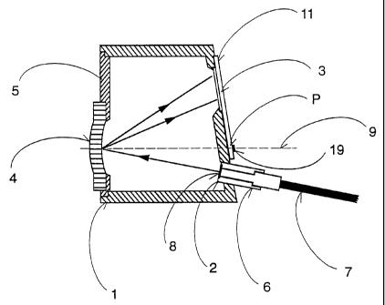
The geometry for the calculation is presented in Fig. 4.
The position of the entry gap on the carrier is denoted with the letter A. The
distance to the centre of the grating M is denoted with Ia. The light beam is
reflected at
the diffraction grating and is deflected according to the equation for a
grating with first
order diffraction:
sin9,=-sin9,.,,+n
wherein 01 denotes the angle of the first order diffraction, 0;,, is the angle
of incidence of
the light beam on the grating, k is the wavelength of the light beam in the
medium, A
denotes the period of the grating, and 9 is used to denote the normal to the
grating.
The distance from the diffraction grating to the measurement point B in the
exit plane (on the diode array) is denoted with -lb. The point of intersection
between the
exit plane and the plane of dispersion is denoted as the x-axis. The zero
point of the x-axis
lies on the normal of the grating 9 and a positive axis is chosen in the
direction of the
measurement point B. The base board 11 is fastened at point P on the carrier
with respect
to the x-axis. The distance between the normal of the grating 9 and point P is
denoted with
hp. The distance on the base board 11 to point B on the diode array 3 or the
detector chip
10 is denoted with hb.
The thermal expansion occurs according to the following equation:
9
CA 02303613 2000-03-31
deT = do(1+ a,A T)
wherein do and doT denote the distances before and after warming by a certain
temperature
difference OT and a is the thermal expansion coefficient of the respective
material. The
distances 1 a, 1 b, and hp are situated on the carrier 1 and expand with the
thermal
expansion coefficient at of the material of the carrier.
The grating constant A expands with the thermal expansion coefficient ag of
the material of the grating and influences the angle 01 of the first order
diffraction as given
by the equation for the grating. The distance hb is situated on the base board
and expands
with the thermal expansion coefficient aa of the base board. The thermal
expansion of the
detector chip 10 situated on the base board and made from semiconductor
material is
negligible because of the small size and a small thermal expansion coefficient
of the
semiconductor material (f.ex., silica a=2.5x10⁻⁶ 1/ K).
For an analysis two drift components are calculated: First, the shift of the
measurement point B along the x-axis Ox, as a result of the thermal expansion
of the
carrier 1 and the grating period A and second, an absolute shift of the diode
array 3 with
respect to the x-axis Ax2. A perfect compensation for the temperature drift is
achieved
when both components are identical over the entire wavelength region of the
measured
spectrum:
Ox, = exZ
The shift Oxl is calculated using the above cited equations. The shift of the
diode array
Ox2 is determined by using the thermal expansion of the carrier I and the base
board 11
(change of hb and hp) and can be expressed with the following equation:
exZ = hpatA T+hbadeT
Since the two components base board and carrier are made from different
materials, it is
possible to fit the temperature drift Axl to that of Ax2 by carefully choosing
the position of
the glueing point P, i.e. the relative distance of-the detector chip 10 along
the x-axis from
the glueing point P on the base board 11. The spectral shift Ox2 of the diode
array is
independent from the wavelength of the measurement light. Thus, by using this
optimization of the position only a constant spectral drift is compensated
over the entire
wavelength region of the measured spectrum. The fastening via the positioning
structures
17, 18, 19 on base board 11 and carrier 1 can be carried out on a straight
line through the
ideal point P perpendicular to the plane of dispersion.
CA 02303613 2000-03-31
The method for an optimum compensation of the temperature drift according
to the described model can be carried out in two steps:
Choice of material for carrier 1 and grating 4 for a certain geometry of the
spectrometer in order to achieve a nearly constant spectral shift Oxl over the
entire
wavelength region of the measured spectrum.
Remaining compensation of the spectral shift for an intermediate wavelength
of the measured spectrum by finding an optimum position of the fastening point
P of the
carrier I and base board 11 of the detector unit 3. Of course, the resulting
fastening point
P has to meet geometrical requirements, i.e. it must be feasible on the
carrier 1.
Otherwise, the choice of material has to be changed accordingly.
The method of compensation is demonstrated using the following example.
Parameters of the spectrometer according to Fig. 4:
measured spectrum: 380 nm - 730 nm
period of grating: 2.1 m
l a= 22.3 mm
lb (380 nm) = 27.61 mm
angle of incidence 6;n : -7.034
angle of first order diffraction 01 (380 nm): 17.521
tilt of the x-axis with respect to the normal of the grating y: -2.946
Preferred materials for the manufacture with thermal expansion coefficients:
grating: plastic material, ag 53x10-6 1/ K
carrier: plastic material, a,=selectable to yield optimum temperature drift
base board, diode array: PCB material, aa=16x10 i 1/ K
The simulation of the thermal expansion yields an optimum thermal expansion
coefficient for the carrier of a~=58x10-6 1/ K for a nearly constant spectral
shift over the
entire spectral region.
The compensation of the remaining temperature drift value for an intermediate
wavelength of X=550 nm yields an optimum position for the fastening point of
0.5 mm
above the normal of the grating.
The resulting spectral temperature drift is below 0.05 nm while being warmed
up by 10 C.
11