Note: Descriptions are shown in the official language in which they were submitted.
CA 02311104 2000-06-02
c~
- 1 - CFO 14526 ~8
Ink Jet Recording Head, and Ink Jet Recording Device
BACKGROUND OF THE INVENTION
Field of the Invention
The present invention relates to an ink jet
recording head for discharging ink to form a desired
image on a material to be recorded, and an ink jet
recording device.
Related Background Art
There has heretofore been known an ink jet
recording method comprising: applying heat and other
energy to ink; causing a state change with a steep
volume change (bubble generation) in the ink;
discharging the ink from a discharge port by the action
force based on the state change; and attaching the ink
to a material to be recorded to form an image, which is
a so-called bubble jet recording method. A recording
device using the bubble jet recording method is, as
disclosed in U.S. Patent No. 4,723,129, generally
provided with a discharge port for discharging ink, an
ink channel communicating with the discharge port, and
an electrothermal converter as energy generating means
disposed in the ink channel to discharge the ink.
According to the recording method, a high-grade
image can be recorded at a high speed and with a low
noise, and a head for performing this recording method
can be provided with highly densely arranged discharge
CA 02311104 2000-06-02
- 2 -
ports for discharging the ink, so that a recorded image
with a high resolution by a small device, an easily
obtainable color image, and many other superior
respects are realized. Therefore, in recent years, the
bubble jet recording method has been utilized in a
printer, copying machine, facsimile machine and many
other office apparatuses, and further utilized in
industrial systems such as textile printing equipment.
Additionally, a recording element for generating
an energy to discharge the ink can be formed using a
semiconductor manufacture process. Therefore, the head
utilizing the bubble jet technique is constituted by
forming the recording element on an element substrate
formed of a silicon substrate, and bonding onto the
element a top plate provided with a groove for forming
the ink channel and formed of polysulfone, another
resin, glass or the like.
Moreover, since the element substrate is formed of
the silicon substrate, not only the recording element,
but also a driver for driving the recording element, a
temperature sensor used for controlling the recording
element in accordance with a head temperature, a drive
controller, and the like are constituted on the element
substrate.
One example of the head substrate is shown, for
example, in Fig. 25. Additionally, Fig. 25 shows the
constitution as the related art of Japanese Patent
CA 02311104 2000-06-02
- 3 -
Application Laid-Open No. 7-256883.
In Fig. 25, an element substrate 900 is provided
with: a plurality of heaters (recording elements) 901,
arranged in parallel, for applying a discharging heat
energy to the ink; power transistors 902 for driving
the respective heaters 901; a shift register 904 to
which image data serially inputted from the outside and
a serial clock synchronous with the data are inputted,
and which latches the image data for each line; a latch
circuit 903 for latching the image data for one line
outputted from the shift register 903 in
synchronization with a latching clock, and transferring
the data in parallel to the power transistor 902; a
plurality of AND gates 915, disposed for the respective
power transistors 902, for applying the output signal
of the latch circuit 903 to the power transistor 902 in
response to an enabling signal from the outside; and
input terminals 905 to 912 for inputting the image
data, various signals, and the like from the outside.
Moreover, the element substrate 900 is provided
with a temperature sensor for measuring the temperature
of the element substrate 900, a resistance sensor for
measuring the resistivity of the respective heaters
901, or another sensor 914.
The head constituted by forming the driver,
temperature sensor, drive controller, and the like on
the element substrate is practically used, and
CA 02311104 2000-06-02
- 4 -
contributes to the enhancement of a recording head
reliability and the reduction in size of the device.
In this constitution, the image data inputted as a
serial signal is converted to a parallel signal by the
shift register 904, and outputted/held by the latch
circuit 903 in synchronization with the latching clock.
When a drive pulse signal (enabling signal for the AND
gate 915) of the heater 901 is inputted via the input
terminal i.n this state, the power transistor 902 turns
on in accordance with the image data, an electric
current flows in the corresponding heater 901, and the
ink of a liquid channel is heated and discharged as a
liquid drop from a nozzle tip end.
Here, in the constitution shown in Fig. 25, a main
body device in the ink jet recording device monitors
the output: of the sensor 914 to detect the resistivity
of the heater 901, and changes a power voltage and
drive pulse width in accordance with the value, so that
a substantially constant energy is applied to the
heater 901.
In the ink jet recording device described in the
Japanese Patent Application Laid-Open No. 7-256883, for
a purpose of reducing the load of the main body device
of the ink jet recording device, it is proposed to
drive the sensor 914, form on the element substrate 900
the drive controller for controlling the drive pulse
width of the heater 901 in accordance with the output
CA 02311104 2000-06-02
- 5 -
from the sensor 914, monitor the resistivity of the
respective heaters 901 and temperature sensor in the
element substrate 900 and detect head property and
state and to change the drive pulse width of the heater
901 in accordance with the property and state.
In recent years, for the ink jet recording device,
there has been an increasing demand for a higher grade
image output in various products and fields. Moreover,
a demand for enhancing a recording speed has also
increased, and the increase of the number of nozzles
for discharging the ink and the shortening of a
recording period have been achieved. As a result, the
number of the recording elements to be simultaneously
driven increases, cost increases because of a necessity
of increasing a power capacity, and additionally in
respect of fluid the simultaneous discharge of much ink
is disadvantageous in performing a stable discharge.
To cope with the problem, it is effective to
reduce the number of simultaneously driven recording
elements by shortening the width of the drive pulse
signal applied to the recording element.
Here, in the conventional example, a head
discharge frequency is about 10 KHz (period of 100 pS),
and about 6 pS per time division in case of a time
division number of 16. In this case, one heat signal
pulse width can be handled at about 4 to 5 uS. Here,
when the time resolution necessary for generating and
CA 02311104 2000-06-02
- 6 -
controlling a heat signal pulse in the head is of the
order of 1/20 to 1/40 of the heat signal pulse, the
feedback to the pulse width by the sensor output can be
performed, and the clock frequency as a reference for
obtaining the resolution is in a range of 5 to 10 MHz
(period of 0.2 uS to 0.1 uS).
Moreover, when the width of the heat pulse signal
is shortened to cope with the increase of a momentary
current by the increase of the nozzle number, and the
high printing speed, for example, at the drive
frequency of 30 KHz and the time division number also
of 16, one time division time is only about 2 NS, and
the time for one time division is much shorter than the
conventional time of about 6 uS. Therefore, in this
case, one heat signal pulse width is requested to be
set to 2 NS or less (about 0.5 to 1.5 uS). The
resolution required for the heat signal in
consideration of the pulse width control is in a range
of 0.01 uS to 0.07 pS, and the reference clock signal
for satisfying this level of the resolution requires a
frequency of 15 MHz to 100 MHz (period of 0.07 uS to
0.01 pS).
When the transfer clock frequency of the image
data is increased (the period is shortened), the
resolution can be enhanced, but the clock signal is
usually supplied to the head from the main body device
of the recording device as shown in Fig. 25, and the
CA 02311104 2000-06-02
_ 7 _
head moving during printing is therefore connected to
the main body device with the relatively long cable of
a flexible substrate or the like. Since a high current
flows in the vicinity of the cable, noises are easily
superposed onto the signal transmitted by the cable,
and there arises a phenomenon in which pulse waveform
rising and falling are lengthened by the inductance
component of the cable (waveform gets blunted)
(specifically, the waveform of Fig. 26A changes to that
of Fig. 26B). This varies the drive time of the
recording element. Moreover, when the drive pulse
signal period becomes shorter, the variation proportion
relatively increases, the influence of the blunted
pulse waveform cannot be ignored, the signal cannot
accurately be received on a head side, and there is a
possibility that malfunction occurs. Moreover, this
also shortens the life of the recording element.
Furthermore, when a high-frequency clock is
transmitted, the cable acts as an antenna and radiation
noise is generated. This radiation noise possibly
causes the malfunction in peripherals.
There is a limitation in the increase of the clock
frequency to shorten the conventional pulse width in
this manner, and it has heretofore been difficult to
set the pulse width to 2 uS or less.
As a technique of eliminating the bluntness of the
transfer clock waveform and reducing radiation noises,
CA 02311104 2000-06-02
_ g _
for example, there is proposed a method of radiating
signal light to a carriage with a head mounted thereon
from a main body device, receiving the signal light on
a carriage side to regenerate an electric signal, and
thus transmitting a clock to the carriage from the main
body device by so-called optical communication.
In this case, however, since the head and carriage
move in accordance with the size of the material to be
recorded, the signal has to be correctly received in
any position. For this purpose the main body device on
a transmission side has to radiate intense light in a
wide range, and has to turn on/off the light at a high
speed. Specifically, since the main body device needs
to pass a large current to a light emitting element for
use in the optical communication, and the drive element
needs to be switched at a high speed, it is difficult
to transmit the clock for the head with the increased
speed and increased nozzles via light.
SUMMARY OF THE INVENTION
The present invention has been developed to solve
the above-described related-art problems, and an object
thereof is to provide an ink jet recording head and an
ink jet recording device which inhibit the bluntness of
a pulse waveform by the transmission of a signal via a
cable, and a radiation noise generated from the cable,
and which cope with high speed and a multiplicity of
CA 02311104 2000-06-02
_ g _
nozzles.
To achieve the above-described object, according
to one aspect of the present invention there is
provided an ink jet recording head comprising: a
plurality of recording elements for applying an energy
to discharge ink; a recording element driver for
driving the plurality of recording elements; a control
circuit for controlling the recording element driver;
and a high resolution reference signal generator using
a plurality of input signals continuously given from
the outside in a predetermined period and generating a
reference signal which has a period shorter than the
predetermined period, so that recording control is
performed by supplying the reference signal to the
control circuit.
According to another aspect of the present
invention there is provided an ink jet recording device
comprising: an ink jet recording head comprising a
plurality of recording elements for applying an energy
to discharge ink, a recording element driver for
driving the plurality of recording elements, and a
control circuit for controlling the recording element
driver; a carriage on which the ink jet recording head
is detachably mounted and which is scanned along the
surface of a material to be recorded; and a main body
device for transmitting a plurality of signals to be
used for a recording control to the ink jet recording
CA 02311104 2000-06-02
- 10 -
head. In the ink jet recording device, the ink jet
recording head comprises a high resolution reference
signal generator for using an input signal continuously
given from the outside in a predetermined period and
generating a reference signal having a period shorter
than the predetermined period, and the recording
control is performed by supplying the reference signal
to the control circuit.
In the above-described ink jet recording device,
since a part of signal period for use in the recording
control inside the ink jet recording head can be
provided with a high resolution, the period of the
signal to be transmitted to the ink jet recording head
in which high speed and a multiplicity of nozzles are
realized can be set to be substantially the same as the
conventional period.
Additionally, "downstream" and "upstream" used in
the description of the present invention are used as
representations regarding a liquid flow direction
toward the discharge port from a liquid supply source
via a bubble generation area (or a movable member), or
regarding the upward direction of the constitution.
BRIEF DESCRIPTION OF THE DRAWINGS
Fig. 1 is a sectional view along a liquid channel
direction, showing the structure of an ink jet
recording head according to one embodiment of the
CA 02311104 2000-06-02
- 11 -
present invention.
Figs. 2A and 2B are sectional views of an element
substrate for use in the ink jet recording head shown
in Fig. 1.
Fig. 3 is a schematic sectional view showing the
element substrate which is cut to longitudinally cross
the main elements of the element substrate shown in
Figs. 2A and 2B.
Figs. 4A and 4B are diagrams showing the circuit
constitution of the element substrate and top plate for
controlling an energy to be applied to a heater in
response to a sensor output.
Fig. 5 is a block diagram showing one constitution
example of a PLL circuit shown in Figs. 4A and 4B.
Fig. 6 is a block diagram showing a signal flow
according to a first embodiment.
Fig. 7 is a plan view showing the constitution of
an ink jet recording device according to one embodiment
of the present invention.
Fig. 8 is a block diagram showing the signal flow
of a second embodiment.
Fig. 9 is a block diagram showing the signal flow
of a third embodiment.
Fig. 10 is a block diagram showing the signal flow
of a fourth embodiment.
Fig. 11 is a block diagram showing the signal flow
of a fifth embodiment.
CA 02311104 2000-06-02
- 12 -
Fig. 12 is a block diagram showing a modification
example of Fig. 11.
Fig. 13 is a block diagram showing further
modification example of Fig. 11.
Fig. 14 is a block diagram showing the signal flow
of a sixth embodiment.
Figs. 15A and 15B are diagrams showing the circuit
constitution of the element substrate and top plate for
controlling an element substrate temperature in
response to the sensor output.
Figs. 16A and 16B are diagrams showing the circuit
constitution of the element substrate and top plate for
utilizing the output of a temperature sensor and
detecting the presence/absence of ink.
Figs. 17A and 17B are diagrams showing the
modification example of the circuit constitution of the
element substrate and top plate shown in Figs. 16A,
16B.
Figs. 18A and 18B are diagrams showing the
modification example of the circuit constitution of the
element substrate and top plate shown in Figs. 16A,
168.
Figs. 19A and 19B are diagrams showing the
modification example of the circuit constitution of the
element substrate and top plate shown in Figs. 16A,
16B.
Figs. 20A and 20B are diagrams showing the
CA 02311104 2000-06-02
- 13 -
modification example of the circuit constitution of the
element substrate and top plate shown in Figs. 16A,
16B.
Fig. 21 is an exploded perspective view of an ink
jet recording head cartridge to which the present
invention can be applied.
Fig. 22 is an schematic constitution diagram of an
ink jet recording device to which the present invention
can be applied.
Fig. 23 is a device block diagram of the ink jet
recording device to which the present invention can be
applied.
Fig. 24 is a diagram showing a liquid discharge
system to which the present invention can be applied.
Fig. 25 is a circuit diagram of a conventional
head element substrate.
Figs. 26A and 26B are explanatory views showing
waveform bluntness.
DETAILED DESCRIPTION OF THE PREFERRED EMBODIMENTS
In the present invention, a high resolution
reference signal generator is constituted, for example,
between a conventional heat signal generator and a
print apparatus body, the print apparatus body
transfers a clock signal of a conventional level
frequency, the high resolution reference signal
generator is formed in a head or carriage part, the
CA 02311104 2000-06-02
- 14 -
frequency of the received clock signal is raised in the
part, and a high resolution reference clock signal is
generated and supplied to the heat signal generator.
Since the frequency of the reference signal is raised
to obtain a high resolution in the head/carriage part
in this manner, a high precision drive signal is
generated and supplied even in a high frequency drive
head, and the feedback of a sensor, and the like in the
head can sufficiently be performed.
The present invention will be described
hereinafter in detail with reference to the drawings.
(First Embodiment)
An ink jet recording head will be described as one
embodiment to which the present invention can be
applied. The head is provided with: a plurality of
discharge ports for discharging ink (liquid); a first
substrate and second substrate, bonded to each other,
for constituting a plurality of liquid channels to
communicate with the respective discharge ports; a
plurality of recording elements, disposed in the
respective liquid channels, for converting an electric
energy to a liquid discharge energy in the liquid
channel; and a plurality of elements or electric
circuits different from one another in function for
controlling a recording element drive condition, and
the elements or electric circuits are distributed to
the first substrate and second substrate in accordance
CA 02311104 2000-06-02
- 15 -
with functions.
Additionally, an example in which a heating
element (heater) is used as the recording element will
be described hereinafter, but a piezoelectric element
for discharging the ink by a piezo-effect may be used
in the recording element. Fig. 1 is a sectional view
along the liquid channel direction of the ink jet
recording head as one embodiment of the present
invention.
As shown in Fig. 1, the ink jet recording head is
provided with: an element substrate 1 in which heaters
2 are arranged in parallel as a plurality of (only one
is shown in Fig. 1 recording elements for applying a
heat energy to generate bubbles in the liquid; a top
plate 3 bonded onto the element substrate 1; an orifice
plate 4 bonded to the front end surfaces of the element
substrate 1 and top plate 3; and a movable member 6
installed in a liquid channel 7 constituted by the
element substrate 1 and top plate 3.
In the element substrate 1, a silicon oxide film
or a silicon nitride film is formed on a substrate of
silicon or the like for a purpose of insulation and
heat accumulation, and an electric resistance layer and
wiring constituting the heater 2 are patterned on the
film. When a voltage is applied to the electric
resistance layer via the wiring, and a current is
passed to the electric resistance layer, the heater 2
CA 02311104 2000-06-02
- 16 -
generates heat.
The top plate 3 constitutes a plurality of liquid
channels 7 for the respective heaters 2 and a common
liquid chamber 8 for supplying liquid to the respective
liquid channels 7, and a channel side wall 9 extending
between a ceiling part and the respective heaters 2 is
integrally disposed. The top plate 3 is constituted of
a silicon-based material, and can be formed by etching
and forming the pattern of the liquid channel 7 and
common liquid chamber 8, or depositing silicon nitride,
silicon oxide or another material of the channel side
wall 9 on the silicon substrate by a known film forming
method such as CVD and then etching and forming the
part of the liquid channel 7.
The orifice plate 4 is provided with a plurality
of discharge ports 5 which are connected to the
respective liquid channels 7 and which communicate with
the common liquid chamber 8 via the respective liquid
channels 7. The orifice plate 4 is also formed of the
silicon-based material and is formed, for example, by
scraping the silicon substrate provided with the
discharge port 5 to obtain a thickness of about 10 to
150 pm. Additionally, the orifice plate 4 is not
necessarily a constitution required for the present
invention, and instead of the orifice plate 4, the top
plate provided with the discharge port may be
constituted by leaving a wall with a thickness
CA 02311104 2000-06-02
- 17 -
corresponding to the thickness of the orifice plate 4
in the tip end surface of the top plate 3 during the
forming of the liquid channel 7 in the top plate 3, and
forming the discharge port 5 in this part.
The movable member 6 is a cantilever-shaped thin
film, disposed opposite to the heater 2, for dividing
the liquid channel 7 into a first liquid channel 7a
communicating with the discharge port 5 and a second
liquid channel 7b including the heater 2, and is formed
of the silicon-based material such as silicon nitride
and silicon oxide.
This movable member 6 is provided with a support
6a on the upstream side of a large flow toward the
discharge port 5 from the common liquid chamber 8 via
the movable member 6 by the liquid discharge operation,
and is disposed opposite to the heater 2 at a
predetermined distance from the heater 2 so as to cover
the heater 2 so that a free end 6b is disposed on a
downstream side with respect to the support 6a. A
bubble generation area 10 is formed between the heater
2 and the movable member 6.
When the heater 2 is heated based on the above-
described constitution, heat acts on the liquid of the
bubble generation area 10 between the movable member 6
and the heater 2, and the bubble is generated on the
heater 2 based on a film boiling phenomenon and grows.
The pressure with the growth of the bubble
CA 02311104 2000-06-02
- 18 -
preferentially acts on the movable member 6, and the
movable member 6 is displaced to open widely on the
side of the discharge port 5 centering on the support
6a as shown by a broken line in Fig. 1. By the
displacement or the displaced state of the movable
member 6, the propagation of the pressure based on the
bubble generation and the growth of the bubble itself
are guided to the side of the discharge port 5, and the
liquid is discharged from the discharge port 5.
Specifically, when the movable member 6 is
disposed on the bubble generation area 10, and provided
with the support 6a on the upstream side (the side of
the common liquid chamber 8) of the liquid flow in the
liquid channel 7 and the free end 6b on the downstream
side (the side of the discharge port 5), the pressure
propagation direction of the bubble is guided to the
downstream side, and the pressure of the bubble
directly and efficiently contributes to the discharge.
Moreover, the bubble growth direction itself is guided
to the downstream direction similarly as the pressure
propagation direction, and the bubble largely grows on
the downstream rather than the upstream. By
controlling the bubble growth direction itself by the
movable member, and controlling the bubble pressure
propagation direction, the fundamental discharge
properties such as discharge efficiency, discharge
force and discharge speed can be enhanced.
CA 02311104 2000-06-02
- 19 -
On the other hand, when the bubble enters an anti-
foaming process, the bubble rapidly disappears by a
synergistic effect with the elastic force of the
movable member 6, and the movable member 6 also finally
returns to an initial position shown by a solid line in
Fig. 1. In this case, to compensate for the reduced
volume of the bubble in the bubble generation area 10,
or to compensate for the volume of the discharged
liquid, the liquid flows from the upstream side, that
is, the side of the common liquid chamber 8, and the
liquid channel 7 is refilled with the liquid, but the
refilling with the liquid is efficiently, rationally,
and stably performed by the returning action of the
movable member 6.
Moreover, the ink jet recording head of the
present embodiment is provided with the circuit and
element for driving the heater 2 and controlling the
driving thereof. These circuit and element are shared
and disposed on the element substrate 1 or the top
plate 3 in accordance with the function. Moreover,
since the element substrate 1 and top plate 3 are
constituted of the silicon material, these circuit and
element can easily and finely be formed using a
semiconductor wafer process technique.
The distribution constitution of the circuit and
element to the element substrate 1 and top plate 3 will
next be described.
CA 02311104 2000-06-02
- 20 -
Figs. 2A and 2B are explanatory views showing the
circuit constitution of the ink jet recording head
shown in Fig. 1, Fig. 2A is a plan view of the element
substrate, and Fig. 2H is a plan view of the top plate.
Additionally, Figs. 2A and 2B show opposite faces.
As shown in Fig. 2A, the element substrate 1 is
provided with the plurality of heaters 2 arranged in
parallel, a driver 11 for driving these heaters 2 in
accordance with image data, an image data transfer
portion 12 for outputting the inputted image data to
the driver 11, and a sensor 13 for measuring a
parameter necessary for controlling the drive condition
of the heaters 2.
The image data transfer portion 12 is constituted
of a shift register for outputting the serially
inputted image data to the respective drivers 11 in
parallel, and a latch circuit for temporarily storing
the data outputted from the shift register.
Additionally, the image data transfer portion 12 may
individually output the image data to the respective
heaters 2, or may divide the arrangement of the heaters
2 into a plurality of blocks and output the image data
by a block unit. Particularly, by providing one head
with a plurality of shift registers and performing the
data transfer from the recording device main body by
distributing and inputting the data to the plurality of
shift registers, it is possible to easily cope with the
CA 02311104 2000-06-02
- 21 -
accelerated printing speed.
A temperature sensor for measuring the temperature
in the vicinity of the heater 2, a resistance sensor
for monitoring the resistivity of the heater 2, or the
like is used as the sensor 13.
When the discharge amount of jetted liquid drops
is considered, the discharge amount is related mainly
with a liquid foam volume. The liquid foam volume
changes with the temperature of the heater 2 and its
vicinity.
Therefore, by measuring the temperature of the
heater 2 and vicinity by the temperature sensor,
applying a small energy pulse (preheat pulse) to such
an extent that no liquid is discharged before applying
a heat pulse to discharge the liquid in accordance with
the result, changing the pulse width of the preheat
pulse and the output timing to adjust the temperature
of the heater 2 and vicinity, and discharging constant
liquid drops, the image grade is maintained.
Moreover, when the energy necessary for foaming
the liquid in the heater 2 is considered, with the
constant radiation condition, the energy is represented
by the product of the energy introduced per the
necessary unit area of the heater 2 and the area of the
heater 2. Therefore, the voltage applied to both ends
of the heater 2, and the current and pulse width
flowing in the heater 2 may be set to the values at
CA 02311104 2000-06-02
- 22 -
which the necessary energy is obtained. Here, the
voltage applied to the heater 2 can be kept
substantially constant by supplying more voltage to the
power source of the ink jet recording device main body.
On the other hand, for the current flowing in the
heater 2, the resistivity of the heater 2 varies with a
lot, or the element substrate 1 because of the
dispersion of the film thickness of the heater 2 in the
manufacture process of the element substrate 1.
Therefore, when the applied pulse width is constant,
and the resistivity of the heater 2 is larger than the
set value, the flowing current value is reduced, the
energy amount introduced to the heater 2 becomes
insufficient, and the liquid cannot adequately be
foamed. Conversely, when the resistivity of the heater
2 is reduced, the current value becomes larger than the
set value even with the same applied voltage. In this
case, an excess energy is generated by the heater 2,
and the damage and short life of the heater 2 are
possibly caused. Therefore, there is another method
comprising: constantly monitoring the resistivity of
the heater 2 by the resistance sensor; changing the
power voltage and heat pulse width in accordance with
the resistivity; and applying a substantially constant
energy to the heater 2. Specifically, the discharge
amount control element for controlling the ink
discharge amount is the heater 2 itself in the
CA 02311104 2000-06-02
- 23 -
constitution.
On the other hand, as shown in Fig. 2B, the top
plate 3 is provided with: grooves 3a, 3b for
constituting the liquid channel and common liquid
chamber as described above; a sensor driver 17 for
driving the sensor 13 disposed on the element substrate
1; and a heater controller 16 for controlling the drive
condition of the heater 2 based on the output result
from the sensor driven by the sensor driver 17.
Additionally, in the top plate 3, a supply port 3c is
opened to communicate with the common liquid chamber in
order to supply the liquid to the common liquid chamber
from the outside.
Furthermore, connecting contact pads 14, 18 for
electrically connecting the circuit, and the like
formed on the element substrate 1 to the circuit, and
the like formed on the top plate 3 are disposed on
opposite sites of the bonded faces of the element
substrate 1 and top plate 3. Moreover, the element
substrate 1 is provided with an external contact pad 15
which constitutes the input terminal of the electric
signal from the outside. The size of the element
substrate 1 is larger than that of the top plate 3, and
the external contact pad 15 is disposed in a position
which is exposed from the top plate 3 when the element
substrate 1 is bonded to the top plate 3.
Here, one example of a procedure of forming the
CA 02311104 2000-06-02
- 24 -
circuits, and the like on the element substrate 1 and
top plate 3 will be described.
For the element substrate 1, first the circuits
constituting the driver 11, image data transfer portion
12 and sensor 13 are formed on the silicon substrate
using a semiconductor wafer process technique.
Subsequently, the heaters 2 are formed as described
above, and finally the connecting contact pads 14 and
external contact pads 15 are formed.
For the top plate 3, first the circuits
constituting the heater controller 16 and sensor driver
17 are formed on the silicon substrate using the
semiconductor wafer process technique. Subsequently,
the grooves 3a, 3b and supply port 3c constituting the
liquid channel and common liquid chamber are formed by
the film forming technique and etching as described
above, and finally the connecting contact pads 18 are
formed.
When the element substrate 1 and top plate 3
constituted as described above are positioned and
bonded, the heaters 2 are disposed for the respective
liquid channels, and the circuits, and the like formed
on the element substrate 1 and top plate 3 are
electrically connected via the respective connecting
pads 14, 18. This electric connection is performed,
for example, by laying metal bumps, and the like on the
connecting pads 14, 18, but other methods may be
CA 02311104 2000-06-02
- 25 -
performed. By performing the electric connection of
the element substrate 1 to the top plate 3 by the
connecting contact pads 14, 18, the above-described
circuits can electrically be connected to one another
simultaneously with the bonding of the element
substrate 1 to the top plate 3. After bonding the
element substrate 1 to the top plate 3, the orifice
plate 4 is bonded to the tip end of the liquid channel
7, so that the ink jet recording head is completed.
Additionally, the ink jet recording head of the
present embodiment includes the movable member 6 as
shown in Fig. 1, and the movable member 6 is also
formed on the element substrate 1 using a
photolithography process after forming the circuits,
and the like on the element substrate as described
above.
When the ink jet recording head obtained in this
manner is mounted on a head cartridge or a recording
device, as shown in Fig. 3, the head is fixed onto a
base substrate 22 with a printed wiring board 23
mounted thereon, and a liquid discharge head unit 20 is
formed. In Fig. 3, the printed wiring board 23 is
provided with a plurality of wiring patterns 24
electrically connected to the head controller of the
recording device, and these wiring patterns 24 are
electrically connected to the external contact pads 15
via a bonding wire 25. Since the external contact pads
CA 02311104 2000-06-02
- 26 -
15 are disposed only on the element substrate 1, a
liquid discharge head 21 can electrically be connected
to the outside similarly as the conventional ink jet
recording head. Here, the example in which the
external contact pads 15 are disposed on the element
substrate 1 has been described, but the pads may be
disposed only on the top plate 3 instead of the element
substrate 1.
As described above, when various circuits, and the
like for the drive and control of the heater 2 are
distributed to the element substrate 1 and top plate 3
by considering the electric bonding of both, these
circuits, and the like are not concentrated on one
substrate, and the ink jet recording head can be
reduced in size. Moreover, by electrically connecting
the circuits, and the like disposed on the element
substrate 1 to the circuits, and the like disposed on
the top plate 3 by the connecting contact pads 14, 18,
the number of parts electrically connected to the
outside of the head is reduced, and the enhancement of
reliability, the reduction of the number of components,
and further size reduction of the head can be realized.
Moreover, by dispersing the above-described
circuits, and the like to the element substrate 1 and
top plate 3, the yield of the element substrate 1 can
be enhanced, and as a result, the manufacture cost of
the ink jet recording head can be lowered.
CA 02311104 2000-06-02
- 27 -
Furthermore, since the element substrate 1 and top
plate 3 are constituted based on the same material of
silicon, the thermal expansion coefficient of the
element substrate 1 equals that of the top plate 3. As
a result, even when the element substrate 1 and top
plate 3 are thermally expanded by the driving of the
heater 2, no deviation occurs in both, and the position
precision of the heater 2 and liquid channel 7 is
satisfactorily maintained.
In the present embodiment, the above-described
circuits, and the like are distributed in accordance
with the functions, and a basic idea for the
distribution will be described hereinafter.
The circuits to be connected to the respective
heaters 2 individually or by a block unit via electric
wiring are formed on the element substrate 1. In the
example shown in Figs. 2A and 2B, this applies to the
driver 11 and image data transfer portion 12. Since
the drive signals are supplied to the respective
heaters 2 in parallel, the wiring needs to be drawn
around for the signals. Therefore, when the circuits
are formed on the top plate 3, the number of
connections of the element substrate 1 to the top plate
3 increases and a possibility of occurrence of
connection defect increases, but the connection defect
of the heaters 2 and the above-described circuits is
prevented by forming the circuits on the element
CA 02311104 2000-06-02
- 28 -
substrate 1.
Analog parts such as the control circuit are
susceptible to a heat influence, and are therefore
disposed on the substrate with no heaters 2 disposed
thereon, that is, the top plate 3. In the example
shown in Figs. 2A and 2B, the heater controller 16
corresponds to this.
The sensor 13 may be disposed on the element
substrate 1 or the top plate 3 as occasion demands.
For example, for the resistance sensor, since the
resistance sensor not disposed on the element substrate
1 has no meaning or the measurement precision is
deteriorated, the sensor is disposed on the element
substrate 1. Moreover, it is preferable to dispose the
temperature sensor on the element substrate 1 in order
to detect the temperature rise by the abnormality of
the heater driving circuit, but when the ink state is
to be judged by the temperature rise via the ink as
described later, the temperature sensor is preferably
disposed on the top plate 3 or both the element
substrate 1 and top plate 3.
Additionally, circuits not connected to the
respective heaters 2 individually or by the block unit
via the electric wiring, a circuit which does not
necessarily has to be disposed on the element substrate
1, a sensor which exerts no influence on the
measurement precision even when disposed on the top
CA 02311104 2000-06-02
- 29 -
plate 3, and the like are formed on the element
substrate 1 or the top plate 3 as occasion demands so
that they fail to be concentrated to either one of the
element substrate 1 and top plate 3. In the example
shown in Figs. 2A and 2B, the sensor driver 17
corresponds to this.
By disposing the respective circuits, sensors, and
the like on the element substrate 1 and top plate 3
based on the above-described idea, the electric
connection number of the element substrate 1 and top
plate 3 is minimized, and additionally the respective
circuits, sensors, and the like can be distributed with
good balance.
The embodiment has been described above with
respect to the basic constitution of the present
invention, and concrete examples of the above-described
circuits, and the like will be described hereinafter.
<Example of Control of Energy applied to Heater>
Figs. 4A and 4B are diagrams showing the circuit
constitutions of the element substrate and top plate in
which the energy applied to the heater is controlled in
accordance with the sensor output.
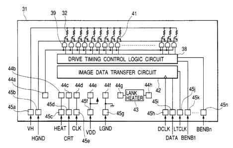
As shown in Fig. 4A, an element substrate 31 is
provided with: heaters 32 arranged in one row; a power
transistor 41 functioning as a driver; an AND circuit
39 for controlling the driving of the power transistor
41; a drive timing control logic circuit 38 for
CA 02311104 2000-06-02
- 30 -
controlling the drive timing of the power transistor
41; an image data transfer circuit 42 constituted of a
shift register and latch circuit; and a rank heater 43
for detecting the resistivity of the heater 32.
The drive timing control logic circuit 38
divisionally drives and energizes the heaters 32 at
deviating times instead of energizing all heaters 32
simultaneously for a purpose of reducing the device
power capacity, and the enabling signal (head drive
time-sharing signal) for driving the drive timing
control logic circuit 38 is inputted via 45k, 45n as
external contact pads.
Moreover, as the external contact pads disposed on
the element substrate 31, in addition to the enabling
signal input terminals 45k, 45n, there are a drive
power input terminal 45a of the heater 32, a ground
terminal 45b of the power transistor 41, input
terminals 45c, 45e for signals necessary for
controlling the energy to drive the heater 32, a logic
circuit drive power terminal 45f, a ground terminal
45g, an input terminal 45i of serial data inputted to
the shift register of the image data transfer circuit
42, a synchronous input terminal 45h of a serial clock
signal, and an input terminal 45j of a latch clock
signal inputted to the latch circuit.
On the other hand, as shown in Fig. 4B, a top
plate 33 is provided with: a sensor drive circuit 47
CA 02311104 2000-06-02
- 31 -
for driving the rank heater 43; a drive signal control
circuit 46 for monitoring the output from the rank
heater 43 and controlling the energy applied to the
heater 32 in accordance with the result; a memory 49
for storing the resistivity data detected by the rank
heater 43 or a code value ranked from the resistivity,
and pre-measured liquid discharge amount properties by
the respective heaters 32 (liquid discharge amount in a
predetermined pulse applied at a constant temperature)
as head information and outputting the information to
the drive signal control circuit 46; and a phase locked
loop (PLL) circuit 50 as a period shortening circuit
for shortening the period of a reference clock CLK
inputted to the drive signal control circuit 46.
Moreover, a the connecting contact pads, the
element substrate 31 and top plate 32 are provided
with: terminals 44g, 44h, 48g, 48h for connecting the
rank heater 43 to the sensor drive circuit 47;
terminals 44b to 44d, 48b to 48d for connecting to the
drive signal control circuit 46 the input terminals 45c
to 45e for signals necessary for controlling the energy
to drive the heater 32 from the outside; a terminal 48a
for inputting the output of the drive signal control
circuit 46 to one input terminal of the AND circuit 39;
and the like.
For example, as shown in Fig. 5, the PLL circuit
50 is constituted of: a phase comparator 71 for
CA 02311104 2000-06-02
- 32 -
detecting the phase difference of two inputted signals;
a low pass filter (LPF) 72 for smoothing the output
pulse of the phase comparator 71; a voltage control
oscillator (VCO) 73 for outputting the pulse signal of
a frequency proportional to the output voltage of the
low pass filter 72; and a divider 74 for dividing the
frequency of the output pulse of the voltage control
oscillator 73.
Since the PLL circuit shown in Fig. 5 operates so
that two signal phases (frequencies) inputted to the
phase comparator 71 agree with each other, the pulse
signal with the frequency (1/N period) N times that of
the input signal determined by the division ratio (1/N)
of the divider 74 can be obtained from the voltage
control oscillator 73.
The PLL circuit 50 is inserted between the
terminal 48d and the drive signal control circuit 46,
and sets the period of the reference clock CLK inputted
via the terminals 48d, 44d by a factor of 1/N.
Additionally, the drive signal control circuit 46 may
operate using a clock DCLK for transferring the image
data, and also in this case, the period of the clock
DCLK is set by the factor of 1/N by the PLL circuit 50
and inputted to the drive signal control circuit 46.
A signal flow in the above-described constitution
will be described. Fig. 6 is a signal flow diagram of
the present embodiment.
CA 02311104 2000-06-02
- 33 -
First, in the device main body, a head drive
control circuit portion generates the reference input
signal for use in generating a heat signal, an image
data transfer signal for use in transferring image data
such as DCLK, DATA and LATCH, and a head drive time-
sharing signal (BENBlton). and outputs these signals to
a head side.
Among these signals, the reference input signal is
inputted to the high resolution reference signal
generating portion 50 before inputted to the drive
signal control circuit 46, and the clock signal CLK
provided with a high resolution is generated from the
reference input signal. The drive signal control
circuit 46 performs correction by the information from
the sensor stored in the memory 49 based on the clock
signal provided with the high resolution and some of
the image data transfer signals, generates a heater
drive-time decision signal, and outputs this heater
drive-time decision signal to the drive timing control
circuit 38 and AND circuit 39.
On the other hand, the image data transfer signal
including the serially inputted image data is inputted
to the image data transfer circuit 42, and outputted as
the latched image data to the drive timing control
circuit 38 and AND circuit 39. Furthermore, head drive
time-sharing signals are inputted to the drive timing
control circuit 38 and AND circuit 39, and a
CA 02311104 2000-06-02
- 34 -
discharging heater is driven by these signals.
Specifically, the resistivity of the heater 32 is
detected by the rank heater 43, and the result is
stored in the memory 49. The drive signal control
circuit 46 decides the rising and falling data of the
drive pulse signal of the heater 32 in accordance with
the resistivity data and liquid discharge amount
property stored in the memory 49, and outputs the data
to the AND circuit 39 via the terminals 48a, 44a. On
the other hand, the serially inputted image data is
stored in the shift register of the image data transfer
circuit 42, latched in the latch circuit by the latch
signal, and outputted to the AND circuit 39 via the
drive timing control circuit 38. Therefore, the pulse
width of the heat pulse is determined in accordance
with the rising and falling data, and the heater 32 is
energized with this pulse width. As a result, the
substantially constant energy is applied to the heater
32.
Here, in the present embodiment, since the PLL
circuit 50 sets the period of the reference clock CLK
for operating the drive signal control circuit 46 by
the factor of 1/N, the drive pulse signal for the ink
jet recording head provided with the accelerated speed
and a multiplicity of nozzles can be generated with the
high resolution and good precision.
As described above, the reference clock CLK is
CA 02311104 2000-06-02
- 35 -
transmitted to the ink jet recording head mounted on
the carriage from the main body device of the ink jet
recording device via the cable of the flexible
substrate or the like. In the present embodiment, even
in the ink jet recording head provided with the
accelerated speed and the multiplicity of nozzles, the
frequency of the reference clock CLK is of the order of
1 MHz to 10 MHz similarly as the conventional art, the
unnecessary radiation noise generated from the cable
can be reduced, the pulse waveform bluntness is
minimized and the malfunction of the ink jet recording
head is prevented.
Moreover, since the frequency of the reference
clock CLK transmitted to the ink jet recording head by
the above-described constitution is of the same degree
as in the conventional constitution, as shown in Fig.
7, the reference clock can also be transmitted by
radiating signal light to an optical data receiver 84
of a carriage 82 with the ink jet recording head
mounted thereon from an optical data transmitter 83 of
a main body 81. In this case, an ink jet recording
device 80 in which the pulse waveform bluntness and
radiation noise are reduced can be obtained.
Additionally, the optical data receiver 84 may be
disposed on the ink jet recording head instead of the
carriage 82.
Moreover, even in a constitution in which a
CA 02311104 2000-06-02
- 36 -
heating element or a piezoelectric element is disposed
in each liquid channel in order to control the position
of a meniscus formed in the discharge port, the ink
discharge amount can be controlled with high precision
by using the clock whose period is set by the factor of
1/N by the PLL circuit 50 and generating the drive
pulse signal.
Additionally, the memory 49 and PLL circuit 50 may
be disposed on the element substrate 31, not on the top
plate 33, if there is a space on the side of the
element substrate 31. In order to solve the problem,
the clock period may be shortened by disposing the PLL
circuit 50 on the substrate different from the element
substrate, or in the carriage which also moves with the
ink jet recording head, although the component cost and
mounting cost slightly increase.
As described above, even when the driving of the
heater 32 is controlled to obtain a satisfactory image
grade, the bubble is generated in the common liquid
chamber. When the bubble moves in the liquid channel
with the refilling with the liquid, there occurs a
disadvantage that no liquid is discharged although the
liquid is present in the common liquid chamber.
To cope with this problem, as not detailed, a
sensor for detecting the presence/absence of the liquid
in the respective liquid channels (particularly in the
vicinity of the heater 32) may be disposed, and further
CA 02311104 2000-06-02
- 37 -
a processing circuit for outputting the result to the
outside when the sensor detects the absence of the
liquid may be disposed on the top plate 33. Moreover,
by forcibly sucking the liquid in the head from the
discharge port on the side of the ink jet recording
device based on the output from the processing circuit,
the bubble in the liquid channel can be removed. As
the sensor for detecting the presence/absence of the
liquid, a sensor for detection by a change of
resistivity via the liquid, or a sensor for detecting
the abnormal temperature rise of the heater when no
liquid is present can be used.
<Example of Element Substrate Temperature Control>
Figs. 15A and 15B are diagrams showing the circuit
constitutions of the element substrate and top plate in
which the temperature of the element substrate is
controlled in response to the sensor output.
In this example, as shown in Fig. 15A, in addition
to a heater 52 for discharging the liquid, for an
element substrate 51, a temperature heater 55 for
heating the element substrate 51 itself to adjust the
temperature of the element substrate 51 as the
discharge amount control element for controlling the
ink discharge amount, and a power transistor 56 as the
driver of the temperature heater 55 are added to the
element substrate 31 shown in Fig. 4A. Moreover, a
temperature sensor for measuring the temperature of the
CA 02311104 2000-06-02
- 38 -
element substrate 51 is used as a sensor 63.
On the other hand, as shown in Fig. 15B, a top
plate 53 is provided with a sensor drive circuit 67 for
driving the sensor 63, a memory 69 for storing the
liquid discharge amount property, and additionally a
temperature heater control circuit 66 for monitoring
the output from the sensor 63 and controlling the
driving of the temperature heater 55 in accordance with
the result. The temperature heater control circuit 66
includes a comparator, compares a threshold value
predetermined based on the temperature required for the
element substrate 51 with the output from the sensor
63, and outputs a temperature heater control signal for
driving the temperature heater 55 when the output from
the sensor 63 is larger than the threshold value. The
temperature required for the element substrate 51 is a
temperature at which the viscosity of the liquid in the
ink jet recording head is in a stable discharge range.
Moreover, terminals 64a, 68a for inputting a
temperature heater control signal outputted from the
temperature heater control circuit 66 to the
temperature heater power transistor 56 formed on the
element substrate 51 are disposed as the connecting
contact pads on the element substrate 51 and top plate
53. The other constitution is similar to the
constitution shown in Figs. 4A and 4B.
According to the above-described constitution, the
CA 02311104 2000-06-02
- 39 -
temperature heater 55 is driven by the temperature
heater control circuit 66 and the temperature of the
element substrate 51 is kept at a predetermined
temperature in accordance with the output result of the
sensor 63. As a result, the liquid viscosity in the
ink jet recording head is kept in the stable discharge
range, and a satisfactory discharge is possible.
Moreover, since the period of the reference clock for
operating the temperature heater control circuit 66 is
shortened by the PLL circuit similarly as the
constitution shown in Figs. 4A and 4B, the drive pulse
signal of the temperature heater 55 can be generated
with a high resolution, and a higher precision
temperature control is possible.
Additionally, the sensor 63 has an output value
dispersion by a solid difference. Furthermore, when an
accurate temperature adjustment is to be performed, the
dispersion may be corrected by storing the correction
value of the output value dispersion as head
information in the memory 69, and adjusting the
threshold value set in the temperature heater control
circuit 66 in accordance with the correction value
stored in the memory 69. Additionally, in the
embodiment shown in Fig. 1, the groove for constituting
the liquid channel 7 is formed in the top plate 3, and
the member (orifice plate 4) provided with the
discharge port 5 is constituted by the member different
CA 02311104 2000-06-02
- 40 -
from those of the element substrate 1 and top plate 3,
but the structure of the ink jet recording head to
which the present invention is applied is not limited
to this.
For example, when a wall is left in the end
surface of the top plate for the thickness of the
orifice plate, and the discharge port is formed in the
wall by an ion beam treatment, an electron beam
treatment, or the like, the ink jet recording head can
be constituted without using the orifice plate.
Moreover, when a channel side wall is formed on the
element substrate instead of forming the groove in the
top plate, the position precision of the liquid channel
with respect to the heater is enhanced, and a top plate
shape can be simplified. The movable member can be
formed on the top plate utilizing the photolithography
process, but when the element substrate is provided
with the channel side wall, the element substrate can
be formed at the same time when the movable member is
formed on the element substrate.
The ink presence/absence detection using the
temperature sensor and the head drive operation in
accordance with the detected result will next be
described with reference to Figs. 16A and 16B to 20A
and 20B.
Figs. 16A and 16B to 20A and 20B are schematic
explanatory views showing the modification examples of
CA 02311104 2000-06-02
- 41 -
the circuit constitution of the element substrate and
top plate of the ink jet recording head of the present
invention, and drawings A are plan views showing the
element substrate and drawings B are plan views showing
the top plate. These drawings A and B show opposite
faces similarly as Figs. 2A and 2B, and a dotted line
in each drawing B shows the position of a liquid
chamber and channel when the top plate is bonded to the
element substrate.
Additionally, in the structure example of the head
shown in Figs. 16A and 16B to 20A and 20B, an element
substrate 401 is provided with a channel wall 401a, but
the structure of the element substrate and top plate
can be applied to any one of the above-described
embodiments. Moreover, unless not particularly
mentioned in the following description, needless to
say, the combination of the respective embodiments
shown in Figs. 16A and 16B to 20A and 20B is also
included in the present invention. Additionally, in
the following description, the part provided with the
common function will be described using the same
reference numerals.
In Fig. 16A, the element substrate 401 is provided
with a plurality of heaters 402 arranged in parallel
for channels as described above, a sub heater 455
disposed in a common liquid chamber, a driver 411 for
driving these heaters 402 in accordance with image
CA 02311104 2000-06-02
- 42 -
data, an image data transfer portion 412 for outputting
the inputted image data to the driver 411, the channel
wall 401a for forming a nozzle, and a liquid chamber
frame 401b for forming the common liquid chamber.
On the other hand, in Fig. 16B, a top plate 403 is
provided with a temperature sensor 413 for measuring
the temperature in the common liquid chamber, a sensor
driver 417 for driving the temperature sensor 413, a
limitation circuit 459 for limiting or stopping the
driving of the heater resistance element based on the
output of the temperature sensor, and a heater
controller 416 for controlling the drive condition of
the heater 402 based on the signals of the sensor
driver 417 and limitation circuit 459, and additionally
a supply port 403a communicating with the common liquid
chamber is opened to supply the liquid to the common
liquid chamber from the outside.
Furthermore, the opposite sites of the bonded
faces of the element substrate 401 and top plate 403
are provided with connecting contact pads 414, 418 for
electrically connecting the circuits formed on the
element substrate 401 to the circuits formed on the top
plate 403. Moreover, the element substrate 401 is
provided with external contact pads 415 as the input
terminals of the electric signals from the outside.
The size of the element substrate 401 is larger than
that of the top plate 403, and the external contact
CA 02311104 2000-06-02
- 43 -
pads 415 are disposed in positions which are exposed
from the top plate 403 when the element substrate 401
is bonded to the top plate 403.
When the element substrate 401 and top plate 403
constituted as described above are positioned and
bonded, the heaters 402 are disposed for the respective
liquid channels, and the circuits, and the like formed
on the element substrate 401 and top plate 403 are
electrically connected via the respective connecting
contact pads 414, 418.
A space of several tens of micrometers is filled
with the ink between a first substrate (element
substrate 401) and a second substrate (top plate 403).
Therefore, when the heating is performed by the sub
heater 455, a difference is produced in the way of heat
conduction to the second substrate by the
presence/absence of the ink. Therefore, when the heat
conduction difference is detected by the temperature
sensor 413 constituted of a diode sensor utilizing PN
bonding, and the like, the presence/absence of the ink
in the liquid chamber can be detected. For example, in
accordance with the detected result by the temperature
sensor 413, when the temperature sensor 413 detects the
abnormal temperature as compared with the presence of
the ink, the limitation circuit 459 limits or stops the
driving of the heater 402, and a signal indicative of
the abnormality is outputted to the main body.
CA 02311104 2000-06-02
- 44 -
Therefore, there can be provided a head which prevents
the physical damage of the head, and constantly
fulfills a stable discharge performance.
Particularly, in the present invention, since the
temperature sensor and limitation circuit can be
manufactured by the semiconductor wafer process, the
element can be disposed in an optimum position, and a
head damage preventing function can be added without
increasing the cost of the head itself.
Figs. 17A and 17B are explanatory views showing
the modification example of Figs. 16A and 16B. The
modification example shown in Figs. 17A and 17B are
different from that of Figs. 16A and 16B in that a
discharging heater, that is, the heater 402 is used
instead of the sub heater. In the modification example
shown in Figs. 17A and 17B, the temperature sensor 413
is disposed in an area on the top plate 403 disposed
opposite to the heater 402, and the ink
presence/absence is detected by detecting the
temperature at which the driving is performed with a
short pulse of a level at which the heater 402 is not
foamed or with a low voltage. In addition to the
detection of the ink presence/absence, the temperature
can be monitored by performing the liquid discharging
operation, and fed back to the driving. The
constitution of the present modification example is
particularly effective when it is difficult to dispose
CA 02311104 2000-06-02
- 45 -
the sub heater in the common liquid chamber. Moreover,
in the present modification example, the heater
controller 416 limits or stops the head driving based
on the output of the temperature sensor 413.
The modification example shown in Figs. 18A and
18B are different from that shown in Figs. 17A and 17B
in that the temperature sensor 413 is disposed to form
a plurality of groups for the different heaters 402 (in
the drawing, 413a, 413b, 413c ... correspond to
individual nozzles). Since the heaters 402 can
selectively be driven, by disposing a plurality of
temperature sensors, the ink state, such as the ink
presence/absence in a finer part, can be detected.
Furthermore, since the temperature sensors are
disposed to establish the one-to-one correspondence
with the respective heaters 402 as in the present
embodiment, the temperature change during the liquid
discharge can be detected by nozzle unit, and the ink
presence/absence in the nozzle, and further the foamed
state can be detected by the temperature. The
detection of a partial non-discharge by the ink
shortage of each nozzle may be performed by disposing a
memory as shown in Figs. 20A and 20B and comparing the
data with the data for the normal discharge held in the
memory, or by comparing the data with the data of a
plurality of adjacent nozzles (for example, when an
abnormal output is made only for 413b among 413a, 413b,
CA 02311104 2000-06-02
- 46 -
413c, ..., abnormality is judged with respect to 413b).
Additionally, in this case, since the respective
temperature sensors 413a, 413b, 413c, ... do not
correspond to the heaters 402 via the electric wiring
connection, there are no problems such as complicated
wiring even when the temperature sensors are disposed
on the top plate 403. Moreover, even when a plurality
of sensors are disposed, the manufacture is performed
by the semiconductor wafer process as in the present
invention, so that no cost rise is caused. Therefore,
this example is particularly preferably employed in a
full line head described later.
The modification example shown in Figs. 19A and
19B are different from the modification example shown
in Figs. 17A and 17B in that both the element substrate
401 and top plate 403 are provided with the temperature
sensors 413a, 413b. When the temperature sensor is
disposed only on either one substrate, the threshold
value indicating the ink presence/absence changes by an
outside air temperature and head state (for example,
immediately after the print end), and it becomes
difficult to perform the control. However, by
measuring a temperature rise difference between two
sensors during heating, the ink state such as the ink
presence/absence can advantageously be detected more
easily and accurately as compared with when the sensor
is disposed only one substrate.
CA 02311104 2000-06-02
- 47 -
The modification example shown in Figs. 20A and
20B are different from the modification example shown
in Figs. 19A and 19B in that a memory 469 is disposed
for storing the temperature change during the heating
of the heating resistance element for the absence and
presence of the ink in the head manufacture process as
head information and outputting the information to the
heater controller 416. By disposing the memory 469 and
comparing the value of the memory 469 with the output
of the sensor, a higher precision detection of ink
presence/absence can be performed.
Of course, as described in the above embodiment,
the memory may hold the pre-measured liquid discharge
amount property by the respective heaters 402 (the
liquid discharge amount in the predetermined pulse
applied at the constant temperature) or the head
information such as the ink for use.
The point of the present invention developed from
the basic constitution has been described above, but in
the present invention, the reference signal from the
print apparatus main body does not have to be requested
individually, or the signal generated from the
reference input signal does not have to be limited to
the heat signal (heater drive-time decision signal).
The example will be describe hereinafter.
(Second Embodiment)
Fig. 8 is a signal flow diagram showing a second
CA 02311104 2000-06-02
- 4$ -
embodiment of the present invention.
The description of the part common with that of
Fig. 6 is omitted.
In the present embodiment, the enabling signal is
generated from the high resolution reference signal and
image data transfer signal in the enabling signal
generator. In the present embodiment, since the
enabling signal does not have to be supplied from the
outside, there can be produced an effect that the
number of signal lines can be reduced. Additionally,
in Fig. 8, the data transfer signal is used to obtain
heat pulse information, but the head includes
nonvolatile memories such as EEPROM, and a constitution
for controlling the memory may be added. Moreover, the
high resolution reference signal inputted to the
enabling signal generator does not have to be
necessarily the same as the high resolution reference
signal inputted to the drive signal control circuit as
long as they are synchronous with each other.
(Third Embodiment)
Fig. 9 is a signal flow diagram showing a third
embodiment of the present invention.
The description of the part common with that of
Fig. 6 is omitted.
In the second embodiment, the enabling signal is
generated from the high resolution reference signal and
image data transfer signal, but in the present
CA 02311104 2000-06-02
- 49 -
embodiment, the enabling signal is generated from the
reference input signal before inputted to the high
resolution reference signal generator and the image
data transfer signal. Since the enabling signal may
have a small resolution with respect to the heat
signal, the original reference input signal may be
utilized without being passed through the high
resolution reference signal generator with respect to
some of the heater drive control signals. Here, when
the resolution is reduced further than necessary, the
constitution of a part for counting the high resolution
reference signals CLK is disadvantageously enlarged
(because the circuit is also enlarged with a larger
count value), and it is also effective to mix the
signals which are passed and are not passed through the
high resolution reference signal generator as occasion
demands.
(Fourth Embodiment)
Fig. 10 is a signal flaw diagram showing a fourth
embodiment of the present invention.
The description of the part common with that of
Fig. 6 is omitted.
In the present embodiment, a data clock signal for
use in data transfer is used generated as the reference
input signal. According to this constitution, it is
possible to reduce the number of signal lines further
than in the second embodiment. In the present
CA 02311104 2000-06-02
- 50 -
embodiment, since the number of clocks is limited by
the number of data to be transferred, it is effective
to mix the signals passed and not passed through the
high resolution reference signal generator as in the
third embodiment.
(Fifth Embodiment)
Fig. 11 is a signal flow diagram showing a fifth
embodiment of the present invention.
The description of the part common with that of
Fig. 6 is omitted.
In the present embodiment, there is disposed an
oscillator for generating the reference input signal in
the head including the carriage. In this case, the
signal line for the reference input signal can be
eliminated. In the present embodiment, however, since
a transmitter is easily influenced by the temperature,
the transmitter is disposed in a carriage part to be
positioned apart from the head heating part. Moreover,
in the present embodiment, the high resolution
reference signal generator is disposed on the carriage,
but the reference signal waveform bluntness by the
drawing of the wiring even on the carriage, and the
radiation noise influence are found in some cases.
Therefore, it is preferable to dispose the high
resolution reference signal generator inside the head
as shown in Fig. 12, or in the head substrate as shown
in Fig. 13.
CA 02311104 2000-06-02
- 51 -
(Sixth Embodiment)
Fig. 14 is a signal flow diagram showing a sixth
embodiment of the present invention.
The description of the part common with that of
Fig. 6 is omitted.
The present embodiment shows a constitution in
which the high resolution reference signal is generated
without using a single signal as the reference input
signal and by using a plurality of other logic signals.
Here, the high resolution reference signal is formed
using a plurality of enabling signals. Specifically,
the reference signals are formed by utilizing the
timing deviations of a plurality of enabling signals,
and the high resolution reference signal higher in
frequency than any other enabling signal is generated.
According to the present constitution, the reference
input signal line can be eliminated.
The embodiments of the main part of the present
invention have been described above, and other
application examples which can preferably be applied to
the present invention will be described hereinafter.
First, an ink jet recording head cartridge with
the ink jet recording head of the present embodiment
mounted thereon will schematically be described.
Fig. 21 is a schematic exploded perspective view
showing the ink jet recording head cartridge including
the above-described ink jet recording head, and the ink
CA 02311104 2000-06-02
- 52 -
jet recording head cartridge is mainly constituted of a
liquid discharge head part 200 and a liquid container
140.
The liquid discharge head part 200 is constituted
of an element substrate 151, a top plate 153 in which a
discharge port is opened, a press spring 128, a liquid
supply member 130, an aluminum base plate (support)
120, and the like. In the element substrate 151, a
plurality of heating resistance bodies for applying
heat to the liquid as described above are arranged in a
row. By bonding the element substrate 151 to the top
plate 153, the liquid channel in which the discharged
liquid is circulated (not shown) is formed. The press
spring 128 is a member for exerting an urging force
onto the top plate 153 in the direction of the element
substrate 151, and the element substrate 151 and top
plate 153 are satisfactorily formed integrally with the
support 120 described later by this urging force. When
the top plate is bonded to the element substrate, for
example, by an adhesive, and the like, no press spring
may be disposed. The support 120 supports the element
substrate 151, and the like, and is further provided
thereon with a printed wiring board 123, connected to
the element substrate 151, for supplying the electric
signal, and a contact pad 124, connected to the device
side, for exchanging the electric signal with the
device side.
CA 02311104 2000-06-02
_. - 53 -
The liquid container 140 contains the liquid to be
supplied to the liquid discharge head part 200.
Disposed outside the liquid container 140 are a
positioning part 144 for disposing a connection member
to connect the liquid discharge head part 200 to the
liquid container 140, and a fixing shaft 145 for fixing
the connection member. The liquid is supplied to
liquid supply paths 131, 132 of the liquid supply
member 130 via the connection member from liquid supply
paths 142, 143 of the liquid container 140, and
supplied to the common liquid chamber via liquid supply
paths 133, 129, 153c of the respective members. Here,
the liquid is supplied to the liquid supply member 130
from the liquid container 140 via two divided paths,
but the path does not have to be necessarily divided.
Additionally, after the liquid is consumed, the
liquid container 140 may be refilled with the liquid
and used. For this, the liquid container 140 may
preferably be provided with a liquid introduction port.
Moreover, the liquid discharge head 200 may be integral
with or separate from the liquid container 140.
Fig. 22 schematically shows the constitution of
the ink jet recording device with the above-described
ink jet recording head mounted thereon. In the present
embodiment, particularly an ink jet recording device
IJRA using the ink as the discharge liquid will be
described. For the carriage (scanner) HC of the ink
CA 02311104 2000-06-02
- 54 -
jet recording device, the head cartridge is mounted so
that the liquid container 140 for containing the ink
and liquid discharge head part 200 are
detachable/attachable., and the carriage
reciprocates/moves in the width direction (direction of
arrows a, b) of a material to be recorded 170, such as
a recording sheet, conveyed by record material
conveying means. Additionally, the liquid container
can be separated from the liquid discharge head part.
In Fig. 22, when the drive signal is supplied to
the liquid discharge means on the carriage HC from
drive signal supply means (not shown) via the flexible
cable, a recording liquid is discharged to the material
to be recorded 170 from the liquid discharge head part
200 in response to the signal.
Moreover, the ink jet recording device of this
example is provided with a motor 161 as a drive source
for driving the record material conveying means and
carriage HC, gears 162, 163 for transmitting the power
to the carriage HC from the drive source, a carriage
shaft 164, and the like. Hy discharging the liquid to
various materials to be recorded by the recording
device, a satisfactory image recording can be obtained.
Fig. 23 is an entire device block diagram for
operating the ink jet recording device to which the ink
jet recording head of the present invention is applied.
The recording device receives print information as
CA 02311104 2000-06-02
- 55 -
the control signal from a host computer 300. The print
information is temporarily saved in an input/output
interface 301 inside the print apparatus, additionally
converted to data which can be processed in the
recording device, and inputted to CPU 302 which also
serves as head drive signal supply means. The CPU 302
uses peripheral units such as RAM 304, processes the
data inputted to the CPU 302 based on a control program
stored in ROM 303, and converts the data to data to be
printed (image data).
Moreover, the CPU 302 generates drive data for
driving a drive motor 306 to move the recording sheet
and head 200 in synchronization with the image data in
order to record the image data in an appropriate
position on the recording sheet. The image data and
motor drive data are transmitted to the head 200 and
drive motor 306 via a head driver 307 and motor driver
305, respectively, and the head and motor are driven at
controlled timings to form the image.
As the material to be recorded which can be
applied to the above-described recording device and to
which the liquids such as the ink are applied, various
types of paper or OHP sheets, plastic materials for use
in compact disks, decorating plates, and the like,
cloth, metal materials such as aluminum and copper,
leather materials such as cowhide, pigskin and
synthetic leather, wood materials such as wood and
CA 02311104 2000-06-02
- 56 -
plywood, bamboo materials, ceramic materials such as
tiles, three-dimensional structures such as sponge, and
the like can be used.
Moreover, examples of the above-described
recording device include a print apparatus for
performing record on various types of paper and OHP
sheets, a plastic recording device for performing
record on the plastic materials such as the compact
disk, a metal recording device for performing record on
the metal plates, a leather recording device for
performing record on the leather, a wood recording
device for performing record on the wood materials, a
ceramic recording device for performing record on the
ceramic materials, a recording device for performing
record on the three-dimensional net structures such as
sponge, and a textile printing device for performing
record on the cloth.
Moreover, as the discharge liquid for use in these
ink jet recording devices, liquids suitable for the
respective materials to be recorded and recording
conditions may be used.
One example of an ink jet recording system will
next be described in which the ink jet recording head
of the present invention is used as a permanent type of
recording head and the recording is performed on the
material to be recorded.
Fig. 24 is a schematic diagram showing the
CA 02311104 2000-06-02
- 57 -
constitution of the ink jet recording device using the
above-described ink jet recording head of the present
invention. For the ink jet recording head of the
present embodiment, a full line type head is provided
with a plurality of discharge ports arranged at an
interval of 360 dpi along a length corresponding to the
recordable width of the material to be recorded, and
four heads 201a to 201d for four colors of yellow (Y),
magenta (M), cyan (C), and black (Bk) are
fixed/supported by a holder 202 in parallel to one
another with a predetermined interval in X direction.
A head driver 307 constituting drive signal supply
means supplies signals to the respective heads 201a to
201d, and the respective heads 201a to 201d are driven
based on the signals. Four color inks Y, M, C, Bk are
supplied as discharge liquids to the respective heads
201a to 201d from ink containers 204a to 204d.
Moreover, head caps 203a to 203d provided therein
with ink absorbing members such as sponge are disposed
below the respective heads 201a to 201d, and
maintenance can be performed on the heads 201a to 201d
by covering the discharge ports of the respective heads
201a to 201d during non-recording.
Reference numeral 206 denotes a conveyance belt
which constitutes conveying means for conveying various
materials to be recorded as described in the above
examples. The conveyance belt 206 is drawn along a
CA 02311104 2000-06-02
- 58 -
predetermined passage, and driven by a driving roller
connected to a motor driver 305.
In the present ink jet recording device, a
pretreatment device 251 and a post-treatment device 252
for performing various treatments on the material to be
recorded before and after performing record are
disposed on the upstream and downstream of a material
to be recorded conveying passage, respectively.
The pretreatment and post-treatment vary in
treatment contents with the types of the materials to
be recorded and inks. For example, the radiation of
ultraviolet rays and ozone is performed as the
pretreatment with respect to the metal, plastic, and
ceramic materials to be recorded, so that the surfaces
are activated to enhance the ink adherence. Moreover,
in the plastic material to be recorded in which static
electricity is easily generated, dust easily adheres to
the surface by the static electricity, and the dust
obstructs a satisfactory record in some cases. To
solve the problem, as the pretreatment, the dust may be
removed from the material to be recorded by using an
ionizer to remove the static electricity from the
material to be recorded. Moreover, when the cloth is
used as the material to be recorded, as the
pretreatment for preventing feathering and enhancing
dyeing degree, the cloth may be provided with a
substance selected from an alkaline substance, a
CA 02311104 2000-06-02
- 59 -
water-soluble substance, a synthetic polymer, a water-
soluble metal salt, urea and thiourea. The
pretreatment is not limited, and a treatment of setting
the temperature of the material to be recorded to a
temperature appropriate for recording may be performed.
On the other hand, examples of the post-treatment
include a thermal treatment of the material to be
recorded with the ink attached thereto, a fixing
treatment for promoting the fixing of the ink by
ultraviolet radiation, and the like, a treatment for
cleaning a non-reacted remaining pretreatment agent,
and the like.
Additionally, in the present example, the heads
201a to 201d have been described using the full line
heads, but they are not limited, and the above
described small head may be conveyed in the width
direction of the material to be recorded to perform
recording. Here, the head in this case also includes
the above-described carriage part.
According to the present invention constituted as
described above, the following effects are produced.
The period of some of a plurality of signals
supplied from the outside is shortened by the period
shortening circuit before the signals are supplied to
the control circuit. Therefore, even when the period
of the signal supplied from the outside is equal to the
conventional period, a drive pulse signal for the ink
CA 02311104 2000-06-02
- 60 -
jet recording head provided with the accelerated speed
and increased nozzles can be generated with the high
resolution and good precision.
Moreover, since the period of some of the signals
for use in the recording control in the ink jet
recording head is shortened, the period of the signal
transmitted to the ink jet recording head provided with
the accelerated speed and increased nozzles can be set
to be the same degree as that of the conventional
period. Therefore, the unnecessary radiation noise
generated from the cable can be reduced, and the
malfunction by the pulse waveform bluntness can be
prevented.