Note: Descriptions are shown in the official language in which they were submitted.
CA 02324273 2000-09-15
WO 99/54960 PCTIUS99/05502
PHASED ARRAY ANTENNA CALIBRATION SYSTEM AND
METHOD USING ARRAY CLUSTERS
BackQround of the Invention
This invention relates generally to phased
array antennas and more particularly to apparatus and
methods used to calibrate such antennas.
As is known in the art, a phased array
antenna includes an array of antenna elements adapted to
produce a plurality of collimated and differently
directed beams of radio frequency energy. These phased
array elements may be corporate fed or space fed. In
either case, the relative amplitude and phase shift
across the array of antenna elements defines the antenna
beam. This relative amplitude and phase state may be
produced by controllable attenuators and phase shifters
coupled to corresponding antenna elements or by
beamforming networks disposed between a plurality of beam
ports and the plurality of antenna elements, where each
beam port corresponds to one of the beams.
In one such beamforming network phased array
antenna system, the beamforming network has a plurality
of array ports each one being coupled to a corresponding
one of the antenna elements through a transmit/receive
module. Each one of the transmit/receive modules
includes an electronically controllable attenuator and
phase shifter. During a receive calibration mode at the
factory or test facility, a source of radio frequency
(RF) energy is placed in the near field of the phased
array antenna elements. The transmit/receive modules are
sequentially activated. When each one of the
transmit/receive module is placed in a receive mode and
is activated, energy received by the antenna element
coupled thereto is passed through the activated
transmit/receive module and through the beamforming
CA 02324273 2000-09-15
WO 99/54960 PCTIUS99/05502
- 2 -
network. The energy at one of the beam ports is detected
during the sequential activation. The detected energy is
recorded for each of the elements of the array in
sequence. The process is repeated for each of the beam
ports. For each antenna element, a least mean square
average is calculated for the detected energy associated
with each of the beam ports. Thus, each antenna element
is associated with an amplitude and phase vector. These
measured/post-calculated vectors are compared with pre-
calculated, designed vectors. If the antenna is operating
properly (i.e., in accordance with its design), the
measured/post-calculated vectors should match the pre-
calculated vectors with minimal error. Any difference in
such measured/post-calculated vector and the pre-
calculated vector is used to provide a control signal to
the controllable attenuator and/or phase shifter in the
module to provide a suitably corrective adjustment. The
calibration is performed in like, reciprocal manner,
during
a transmit calibration mode at the factory or test
facility.
Thus, in either the transmit or receive
calibration modes, errors in the relative phase or
amplitude are detected and the controllable attenuator
and/or phase shifter in the module is suitably adjusted.
While such technique is suitable in a factory or test
facility environment, the use of separate external
transmit and receive antennas may be impractical and/or
costly in operational environments. For example, when
the antenna is deployed in the field it is sometimes
necessary to re-calibrate the antenna after extensive
use. Examples of such environments include, but are not
limited to, outer space as where the antenna is used in a
satellite, on aircraft including fixed wing, rotary wing,
and tethered, and on the earth's surface.
CA 02324273 2000-09-15
WO 99/54960 PCT/US99/05502
- 3
A paper entitled "Phased Array Antenna Calibration
and Pattern Predication Using Mutual Coupling
Measurements" by Herbert M. Aumann, Alan J. Fenn, and
Frank G. Willwerth published in IEEE Transactions on
Antennas and Propagation, Vol. 37, July 1989, pages 844-
850, develops mathematically and demonstrates a
calibration and radiation pattern measurement technique
which takes advantage of the inherent mutual coupling in
an array, by transmitting and receiving all adjacent
pairs of radiating elements through two independent
beamformers (corporate feeds). The technique utilizes an
internal calibration source.
Summary of the Invention
In accordance with one feature of the
invention, apparatus and method are provided for testing
a phased array antenna. The antenna includes a plurality
of antenna elements and a plurality of transmit/receive
modules. Each one of the transmit/receive modules is
coupled to a corresponding one of the antenna elements.
The apparatus includes a calibration system having: an RF
input port; an RF detector port; an RF detector coupled
to the RF detector port; and an RF source connected to
the RF input port. A switch section is included for
sequentially coupling the antenna elements and the
transmit/receive modules coupled thereto selectively to
either: (a) the detector port during a receive
calibration mode; or, (b) to the RF test input port
during a transmit calibration mode. One, or more, (i.e.,
a predetermined set) of the plurality of antenna elements
(i.e., calibration antenna elements) is also coupled to
the switch section. The switch section couples each
calibration antenna element selectively to either: (a)
the RF test input during the receive calibration mode;
or, (b) the RF detector port during the transmit
calibration mode.
CA 02324273 2000-09-15
WO 99/54960 PCTIUS99/05502
- 4 -
In accordance with another feature of the
invention, apparatus and method are provided for testing
a phased array antenna having a beamforming network. The
beamforming network includes a plurality of array ports
and a plurality of beam ports. A plurality of antenna
elements and a plurality of transmit/receive modules are
included. Each one of the modules is coupled between a
corresponding one of the antenna elements and a
corresponding one of the array ports. A calibration
system is provided having: an RF input port; an RF
detector port; an RF detector coupled to the RF detector
port; and an RF source connected to the RF input port. A
switch section is included for sequentially coupling each
one of the antenna elements through the beam forming
network and the one of the transmit/receive modules
coupled thereto selectively to either: (a) the detector
port during a receive calibration mode; or, (b) to the RF
test input port during a transmit calibration mode. The
switch section includes a switch for selectively coupling
a predetermined one of the antenna elements (i.e., a
calibration antenna element) selectively to either: (a)
the RF test input of the calibration system during the
receive calibration mode through a path isolated from the
beamforming network; or, (b) to the detector port during
the transmit calibration mode through a path isolated
from the beamforming network. With such an arrangement,
undesired coupling to the calibration antenna element
through the beamforming network is eliminated.
In accordance with still another feature of
the invention, the array of antenna elements is arranged
in clusters, each one of the clusters having a
predetermined antenna element (i.e, a calibration antenna
element). With such an arrangement, each cluster is
calibrated with the calibration antenna element in such
cluster thereby enabling a relatively small dynamic range
CA 02324273 2006-06-05
78625-4
- 5 -
variation among the antenna elements in such cluster during
the calibration of such cluster.
According to one aspect of the present invention,
there is provided an antenna system, comprising: a
calibration system having: an RF input port; an RF detector
port; an RF detector coupled to the RF detector port; and an
antenna element port; a beamforming network having a
plurality of array ports and a plurality of beam ports; a
plurality of antenna elements grouped in clusters; a
plurality of transmit/receive modules, each one being
coupled between a corresponding one of the antenna elements
and a corresponding one of the array ports; and a switch
section for sequentially coupling each one of the antenna
elements through the beam forming network and the one of the
transmit/receive modules coupled thereto selectively to
either: (a) the detector port during a receive calibration
mode; or, (b) to the RF input port during a transmit
calibration mode; wherein the switch section includes a
switch for coupling a predetermined one of the antenna
elements selectively to either: (a) the RF input of the
calibration system during the receive calibration mode
through a path isolated from the beamforming network; or,
(b) to the detector port during the transmit calibration
mode through a path isolated from the beamforming network;
and wherein an antenna element coupled to the detector port
during the receive calibration mode, or to the RF input port
during the transmit calibration mode, and the predetermined
one of the plurality of antenna elements are disposed in a
common one of the clusters of the plurality of antenna
elements.
CA 02324273 2006-06-05
78625-4
- 5a -
According to another aspect of the present
invention, there is provided a method for calibrating an
antenna system having a plurality of antenna elements
grouped in clusters, a beamforming network having a
plurality of array ports and a plurality of beam ports, and
a plurality of transmit/receive modules, each one being
coupled to a corresponding one of the array ports and to a
corresponding one of the plurality of antenna elements,
comprising the steps of: providing a calibration system
having: an RF input port; an RF detector port; an RF
detector coupled to the RF detector port; and an antenna
element port; sequentially coupling each one of the antenna
elements in a selected one of the plurality of clusters of
antenna elements through the beam forming network and the
one of the transmit/receive modules coupled thereto
selectively to either: (a) the detector port during a
receive calibration mode; or, (b) the RF test input port
during a transmit calibration mode; and coupling a
predetermined one of the plurality of antenna elements in
the selected cluster selectively to either: (a) the RF test
input during the receive calibration mode through a path
isolated from the beam forming network; or, (2) the detector
port during the transmit calibration mode through a path
isolated from the beam forming network.
CA 02324273 2006-06-05
78625-4
- 5b -
Brief Description of the Drawing
Other features and advantages of the invention, as
well as the invention itself, will become more readily
apparent when taken together with the following detailed
description and the accompanying drawings, in which:
FIG. 1 is a block diagram of a phased array antenna
system and calibration system therefore in accordance
with the invention;
FIG. 2 is a front view of the aperture of the
phased array antenna system of FIG. 1 in accordance with
one embodiment of the invention;
FIG. 3 is a block diagram of the phased array
antenna system and.calibration system therefore of FIG.1
shown in the receive calibration mode;
FIG. 4 is a block diagram of the phased array
antenna system and calibration system therefore of FIG.1
shown in the transmit calibration mode; and
FIG. 5 is a front view otthe aperture of the
phased array antenna system of FIG. 1 in accordance with
another embodiment of the invention.
Description of the Preferred Embodiments
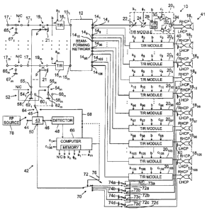
Referring now to FIG. 1, a phased array antenna
system 10 is shown to include a beamforming network 12
having a plurality of, here one hundred and six, array
ports 141-14106 and a plurality of, here m, beam,ports 151-
15m. Each one of the beam ports 151-15m is coupled to a
corresponding one of a plurality of antenna ports 171-17,
through a corresponding one of a plurality of
transmit/receive amplifier sections 161-16,, respectively,
and a corresponding one of a plurality of directional
couplers 191-19n,, respectively, as indicated. Each one of
the directional couplers 191-19, has one port terminated
in a matched load, 21, as indicated. Each one of the
CA 02324273 2000-09-15
WO 99/54960 PCTIUS99/05502
-6-
amplifier sections 161-16,, may be individually gated "on"
(i.e., activated) or "off" in response to a control
signal on a corresponding one of a plurality of lines al-
a,n, respectively, as indicated. Further, the plurality of
amplifier sections 151-15, may be placed in either a
receive state or a transmit state selective in response
to a control signal on line b. (This may be performed by
a transmit/receive (T/R) switch, not shown, included in
each of the amplifier sections 161-16,,,. )
Each one of a plurality of, here one hundred and
six, antenna elements 18,-18106 is coupled to a
corresponding one of the plurality of array ports 141-14106
through a corresponding one of a plurality of
transmit/receive modules 201-20106, respectively, as shown.
Each one of the plurality of transmit/receive modules 201-
20106 is identical in construction and includes serially
connected electronically controllable attenuator 22 and
phase shifter 24, as shown. The attenuator 22 and phase
shifter 24 are connected to a transmit/receive (T/R)
switch 25 through a series of transmit amplifiers 30 in a
transmit path and a series of receive amplifiers 32 in a
receive path. Each of the T/R switches is controlled by
the control signal on line b (which is also fed to the
amplifier sections 161-16,õ as described above) . Each one
of the amplifiers 30, 32 is gated "on" (i.e., activated)
or "off" by a control signal on a corresponding one of
the lines cl-c106, respectively, as indicated. The
amplifiers 30, 32 are coupled to a circulator 34, as
shown. The circulator 34 in each one of the
transmit/receive modules 201-20106 is coupled to a
corresponding one of the antenna elements 181-18106,
respectively, as shown.
More particularly, the radiating face of the array
antenna 10 is shown in FIG. 2. Here, the array antenna
includes one hundred and six antenna elements 181-18106
CA 02324273 2000-09-15
WO 99/54960 PCTIUS99/05502
- 7 -
labeled 001 through 106, for example. Four of the
antenna elements 181-18106, here the antenna elements
labeled 001, 009, 097 and 106 are in predetermined
positions at the periphery of the array face, for reasons
to be discussed. Thus, here there are eight staggered
columns COL1-COL8 of antenna elements 181-18106, in this
illustrative case.
Referring again to FIG. 1, each one of the antenna
elements 181-18106 is here configured as a circularly
polarized antenna element, for example. Therefore, each
antenna element has a right-hand circular polarized feed
(RHCP) and a left-hand circular polarized feed (LHCP).
Here, each one of the right-hand circular polarized feeds
(RHCP) is coupled to a corresponding one of the
circulators 34, as shown. The left hand circular
polarized feed (LHCP) of all but the predetermined four
of the antenna elements 181-18106, here the antenna
elements labeled 001, 009, 097 and 106 are terminated in
matched load impedances 40, as indicated. These
predetermined four of the antenna elements 181-18106 are
calibration antenna elements and are mutually coupled to
the plurality of antenna elements 181-18106 through the
antenna aperture 41. The calibration elements 181-18106
may be arranged in either edge (illustrated) or cluster
arrangements, in order to minimize the calibration errors
and maximize the antenna operation in "normal" mode. In
the edge coupled configuration, calibration elements
occupy the outer edge of the antenna aperture, while in a
cluster arrangement, the aperture is subdivided into
separate regions or clusters, with calibration elements
at the centers. The calibration elements 181-18106 may use
orthogonal circularly polarized ports (illustrated) of a
directional coupler, or dedicated elements as the
calibration element port. Dedicated elements are used as
calibration elements and are not used in "normal" mode,
CA 02324273 2000-09-15
WO 99/54960 PCT/US99/05502
- 8 -
being connected to the calibration components and not to
the "normal" component chain. When used as orthogonal
circularly polarized ports in an edge arrangement, the
left hand circular polarized feed (LHCP) of the
predetermined four of the calibration antenna elements
181-18106, here the antenna elements 181, 189, 1897; and 18106
(i.e., labeled 001, 009, 097 and 106) are coupled to a
calibration system 42, as indicated.
More particularly, the calibration system 42
includes a switch 43 having: an RF input port 44; a
beamforming network port 45; an RF detector port 46; an
RF detector 48 coupled to the RF detector port 46; and an
antenna element port 50. A switch section 52 is
provided. The switch section 52 has a plurality of
switches 541-54m, each one having a first terminal 551-55Rõ
respectively, coupled to a port, P, of a corresponding
one of the directional couplers 191-19, respectively, as
indicated. Each one of the switches 541-54 is adapted to
couple first terminals 551-55, to either second terminals
581-58m or third terminals 601-60,,,, respectively, as
indicated, selectively in response to a control signal on
"normal mode"/"calibration mode" line N/C, as shown.
Each of the second terminals 58,-58m is coupled to a
matched load 621-62,õ respectively, as shown and each one
of the third terminals 601-60m is coupled to a selector
switch 64, as indicated. The operation of the switches
52 and 64 will be described in more detail hereinafter.
Suffice it to say here, however, that when in the normal
operating mode, computer 66 produces a control signal on
line N/C to thereby enable switches 541-54, to couple
terminals 551-55m to matched loads 621-62,õ. On the other
hand, when in the calibration mode, computer 66 produces
a control signal on line N/C to thereby enable switches
541-54, to couple terminals 551-55, to terminals 601-60,;
i.e., to inputs of the selector switch 64. (It should
CA 02324273 2000-09-15
WO 99/54960 PCT/US99/05502
- 9 -
also be noted that during the calibration mode, antenna
ports 171-17R, are coupled, via switches 651-65,, to matched
loads 671-67,õ respectively, as indicated; otherwise, as
in the normal node, switches 651-65m couple antenna ports
171-17, to ports 17' 1-17' m, respectively, as shown.)
When in the calibration mode, the computer 66
produces a control signal on bus 68 so that beamforming
network port 45 becomes sequentially coupled, through
switch 64, to terminals 601-60m. Here, each one of the
terminals 601-60m is, because of the operation of switch
64, coupled to beamforming network port 45 for a period
of time, T.
It is also noted, for reasons to be described
hereinafter, that when terminals 601-60, become
sequentially coupled to beamforming network port 45, the
computer 66 produces the control signals on lines al-am to
sequentially activate a corresponding one of the
transmit/receive amplifier sections 161-16,. Thus, when
terminals 60,-60m become sequentially coupled to port 45,
modules 16,-16m become sequentially activated in
synchronism therewith. The result is that port 45
becomes sequentially electrically coupled to beam ports
151-15m for each of m periods of time, T.
It should also be noted that during the calibration
mode, the computer 66 produces signals on lines cl-c106 to
sequentially activate transmit/receive modules 201-20106,
respectively, during each of the periods of time, T.
Thus, for example, when port 45 is coupled to beam port
151 for the period of time T, the modules 201-20106 become
sequentially activated for a period of time T/106, or
less. Thus, during each one of the m periods of time, T,
the antenna elements 181-18106 become sequentially
electrically coupled to array ports 14,-14106,
respectively.
CA 02324273 2000-09-15
WO 99/54960 PCT/US99/05502
- 10 -
As noted above, each one of the antenna elements
181-18106 has a pair of feeds; an RHCP feed and an LHCP
feed. As described above, each one of the LHCP feeds,
except for those of antenna elements 181, 189, 1897 and
18106 are terminated in matched loads 40, as indicated.
The LHCP feeds of antenna elements 181, 189, 1897 and 18106
are coupled to a selector switch 70 though a switching
network 72, as indicated. More particularly, the
switching network 72 includes switches 72a-72d having:
first terminals 73a-73d coupled to the LHCP feeds of
antenna elements 181, 189, 1897 and 18i06, respectively, as
shown; second terminals coupled to matched loads 74a-74d,
respectively, as shown; and third terminals coupled to
selector switch 70, as shown. During the normal mode,
the switches 72a-72d, in response to the signal on line
N/C (described above) terminate the LHCP
feeds of antenna elements 181, 189, 1897 and 18106 in
matched loads 74a-74d, respectively. During the
calibration mode, the LHCP feeds of antenna elements 181,
189, 1897 and 18106 are coupled to selector switch 70, as
indicated. The function of selector switch 70 will be
described in more detail hereinafter. Suffice it to say
here however that four predetermined calibration antenna
elements 181, 189, 1897 and 18106 are used for redundancy.
That is, the calibration, to be described, may be
performed using only one of the four predetermined
calibration antenna elements 18õ 189, 1897 and 18106;
however, in case of a failure in one, any of the three
others may be used. The one of the four predetermined
calibration antenna elements 181, 189, 1897 and 18106 to be
used is selected by a control signal produced by the
computer 66 on bus 76.
It should be noted that calibration is performed
for both a transmit mode and for a receive mode. During
the receive calibration mode RF energy from source 78 is
CA 02324273 2000-09-15
WO 99/54960 PCT/US99/05502
- 11 -
fed to one of the four predetermined calibration antenna
elements 181, 189, 1897 and 18106. For example, and
referring to FIG. 3, RF source 78 is coupled through
ports 44 and 50 of switch 43 and switch 76 selects one of
the calibration antenna elements, here, for example,
element 181. It is noted that in the receive calibration
mode, switch 43 is configured as indicated; i.e., with
port 44 being electrically coupled to port 50 and with
port 45 being electrically coupled to port 46. In the
transmit calibration mode, as shown in FIG. 4, switch 43
is configured as indicated; i.e., with port 44 (which is
electrically coupled to the RF source 78) being
electrically coupled to port 45 and with port 46 being
electrically coupled to port 50.
Thus, in summary, during the calibration mode, the
calibration system 42 sequentially couples each one of
the antenna elements 181-18106 through the beamforming
network 12 and the one of the transmit/receive modules
20,-20106 coupled thereto selectively to either: (a) the
detector port 46 during a receive calibration mode, as
indicated in FIG. 3; or, (b) to the port 44 during a
transmit calibration mode (FIG. 4). The switch section
42 includes the selector switch 70 for selectively
coupling the left-hand circular polarized feed (LHCP) of
one of the four predetermined calibration antenna
elements labeled 001, 009, 097 and 106 in FIG. 1, during
each test mode selectively to either: (a) the port 44
during the receive calibration mode, as shown in FIG. 3,
through a path 80 isolated from the beamforming network
12; or, (b) to the detector port 46 during the transmit
calibration mode, as shown in FIG. 4, through the path 80
isolated from the beamforming network 12.
It is noted that the four predetermined calibration
antenna elements 181, 189, 1897 and 18106 may be disposed in
a peripheral region of the array of antenna elements
CA 02324273 2000-09-15
WO 99/54960 PCT/US99/05502
- 12 -
(FIG. 2). With such an arrangement, the dynamic range of
the RF signals coupled to the RF detector are minimized
for the operating modes of the antenna.
Consider now the calibration of the phased array
antenna 10, at the factory, or test facility, during a
receive calibration mode. Here, the RF source 78 is
decoupled from port 44, such port 44 being terminated in
a matched load, not shown. Switches 541-54,õ switches
72a-72a and switches 651-65, are placed in the normal mode
thereby: (1) terminating the ports P of directional
couplers 191-19, in matched loads 621-62nõ respectively;
(2) terminating the LHCP feeds of antenna elements 181,
189, 1897 and 18106 in matched loads 74a-74d, respectively;
and electrically coupling antenna ports 171-17, to ports
17'1-17'm, respectively. A source of radio frequency (RF)
energy, not shown, is placed in the near field of the
phased array aperture 41. One of the transmit/receive
amplifier sections 161-16, for example section 161, is
activated and placed in the receive mode. The
transmit/receive modules 202-20106 are placed in the
receive mode and are sequentially activated. When each
one of the transmit/receive modules 201-20106 is placed in
a receive mode and is activated, energy received by the
antenna element coupled thereto is passed through the
activated transmit/receive module 201-20106 and through the
beamforming network 12. The energy at one of the ports
17'1-17',,õ here in this example port 17'1 is detected
during the sequential activation by a detector, not
shown, coupled to port 17'1. The magnitude and phase of
the detected energy at port 17', is recorded. The process
is repeated for each of the other ports 17'2-171,. For
each one of the antenna elements 181-18106, a least mean
square average is calculated for the detected energy
associated with each of the m ports 17'1-17',. Thus,
after the least mean square averaging, each one of the
CA 02324273 2000-09-15
WO 99/54960 PCTIUS99/05502
- 13 -
antenna elements 181-18106 is associated with an amplitude
and phase vector. Each one of the one hundred and six
measured/post-calculated receive vectors are compared
with corresponding ones of one hundred and six pre-
calculated, designed receive vectors. If the antenna is
operating properly (i.e, in accordance with its design),
the measured/post-calculated receive vectors should match
the pre-calculated receive vectors, within a small error.
Any difference in such measured/post-calculated receive
vector and the pre-calculated receive vector for each of
the one hundred and six antenna elements is used to
provide a control signal to the controllable attenuator
22 and/or phase shifter 24 in the transmit/receive module
201-20106 coupled to such one of the antenna elements 181-
18106, respectively, to provide a suitably corrective
adjustment during the antenna's receive mode. After the
corrective adjustments have been made, the antenna system
10 is calibrated for the receive mode.
The calibration is performed in like, reciprocal
manner, during a transmit calibration mode at the factory
or test facility. That is, a receiving antenna, not
shown, is placed in the near field of the phased array
antenna elements. The transmit/receive modules 201-20106
are sequentially activated with an RF source, not shown,
fed to one of the ports 17' 1-17',õ for example port 17' 1.
When each one of the transmit/receive modules 201-20106 is
placed in a transmit mode and is activated, energy is
transmitted by the antenna element 181-18106 coupled
thereto and received by the receiving antenna, not shown.
The energy received at the receiving antenna, not shown,
is detected during the sequential activation. The
amplitude and phase of the detected energy is recorded
and one hundred and six transmit vectors are calculated;
one for each of the antenna elements 181-18106. The
process is repeated with the RF being coupled
CA 02324273 2000-09-15
WO 99/54960 PCT/US99/05502
- 14 -
sequentially to each of the other ports 17'Z-17', Thus,
after all m ports have been used, each one of the antenna
elements 181-18106 will have associated with it a set of m
transmit vectors. The m transmit vectors in each set are
least mean square averaged to produce, for each one of
the antenna elements 181-18106 a measured/post-calculated
transmit vector. These measured/post-calculated transmit
vectors are compared with pre-calculated, designed
transmit vectors. If the antenna is operating properly
(i.e, in accordance with its design), the measured/post-
calculated transmit vectors should match the pre-
calculated transmit vectors, within a small error. Any
difference in such measured/post-calculated transmit
vector and the pre-calculated transmit vector for each of
the one hundred and six antenna elements is used to
provide a control signal to the controllable attenuator
22 and/or phase shifter 24 in the transmit/receive module
201-20106 coupled to such one of the antenna elements 181-
18106, respectively, to provide a suitably corrective
adjustment during the antenna's transmit mode. After the
corrective adjustments have been made, the antenna system
10 is calibrated for the transmit mode.
Once the attenuators and/or phase shifters have been
corrected for both the transmit and receive modes, and
with the phased array system still in the factory, or
test facility, as the case may be (i.e., shortly after
the above just-described calibration procedure) the
calibration system 42 is coupled to the antenna system,
as described in connection with FIGS. 1, 3 and 4 to
determine the coupling coefficients between each one of
the plurality of antenna elements 181-18106 and each one of
the four predetermined calibration antenna elements 181,
189, 1897 and 1810E. Thus, during the receive calibration
mode described in connection with FIG. 3, RF source 78 is
coupled through ports 44 and 50 of switch 43 and switch
CA 02324273 2000-09-15
WO 99/54960 PCT/US99/05502
- 15 -
70 selects one of the calibration antenna elements, here,
for example, element 181. It is noted that in the receive
calibration mode, switch 43 is configured as indicated;
i.e., with port 44 being electrically coupled to port 50
and with port 45 being electrically coupled to port 46.
The switch 70 couples the RF source 78 to one of the four
calibration antenna elements 181, 189, 1897 and 18106, here
for example, antenna element 181. The energy is
transmitted by antenna element 181 and is coupled to the
antenna elements 181-18106 through mutual coupling at the
antenna aperture 41. Concurrently, each one of the
amplifier sections 161-16, is activated and the switching
section 64 operates as described above to sequentially
couple each one of the beam ports 151-15, to port 45 for
the period of time, T. During each of the m periods of
time T, the modules 201-20106 are sequentially activated
and placed in a receive mode so that detector 48
produces, for each one of the one hundred and six antenna
elements 181-18106 amplitude and phase receive vectors.
Each m phase vectors associated for each one of the
antenna elements 181-18106 are least mean square averaged
to produce a receive vector for each one of the antenna
elements. Because the antenna 10 had just been
calibrated, these "calibrated" receive vectors provide a
standard against which deviations in the future may be
measured. These "calibrated" receive vectors are stored
in a memory in computer 66. The process is repeated for
the other three calibration antenna elements 181, 189, 189,
and 18106. Thus, at the end of this receive calibration
mode, the memory in computer 66 stores four sets of
"calibrated" receive vectors, one set for each of the
four calibration antenna elements 189, 1897 and 18106.
The calibration system is then placed in the
transmit calibration mode described above in connection
with FIG. 4. The RF source 78 is coupled through ports
CA 02324273 2000-09-15
WO 99/54960 PCT/US99/05502
- 16 -
44 and 45 to switch 64 and port 50 is coupled to switch
70. Switch 70 selects one of the calibration antenna
elements, here, for example, element 181. It is noted
that in the transmit calibration mode, switch 43 is
configured as indicated; i.e., with port 44 being
electrically coupled to port 45 and with port 50 being
electrically coupled to port 46. The switch 70 couples
the RF source 78 to one of the four calibration antenna
elements 18õ 189, 189, and 18106, here for example, antenna
element 181. Concurrently, each one of the amplifier
sections 161-16n, is activated and the switching section 64
operates as described above to sequentially couple each
one of the beam ports 151-15, to the RF source 78 for the
period of time, T. During each of the m periods of time
T, the modules 201-20106 are sequentially activated and
placed in a transmit mode so that detector 48 produces,
for each one of the one hundred and six antenna elements
181-18106 m amplitude and phase transmit vectors. Each m
phase vectors associated for each one of the antenna
elements 181-18106 are least mean square averaged to
produce a transmit vector for each one of the antenna
elements. Because the antenna 10 had just been
calibrated, these "calibrated" transmit vectors provide a
standard against which deviations in the future may be
measured. These "calibrated" transmit vectors are stored
in a memory in computer 66. The process is repeated for
the other three calibration antenna elements 189, 1897 and
18106. Thus, at the end of this transmit calibration
mode, the memory in computer 66 stores four sets of
"calibrated" transmit vectors, one set for each of the
four calibration antenna elements 181, 189, 1897 and 18106.
After the antenna system 10 has operated in the
field for a sufficient period of time where re-
calibration is required, the calibration system 42 is
used to generate sets of "measured" transmit and receive
CA 02324273 2000-09-15
WO 99/54960 PCTIUS99/05502
- 17 -
vectors. These newly generated "measured" transmit and
receive vectors are generated using the calibration
system 42 in the same manner described above in the
factory or test facility to produce the four sets of
calibrated" received vectors and four sets of "transmit"
vectors which are stored in the memory of computer 66.
If the antenna system is in calibration, the four sets of
"calibrated" receive vectors and the four sets of
"transmit" vectors, stored in the memory of computer 66,
should match the newly generated four sets of "measured"
receive vectors and the four sets of "measured" transmit
vectors within a small margin. Any substantial
difference in any vector in the matrix is used to compute
a gain and/or phase correction which is fed to the
appropriate attenuator 22 and/or phase shifter 24 of the
appropriate transmit/receive module 201-20106.
Referring now to FIG. 5, an alternative positioning
of the predetermined calibration antenna elements is
shown. More particularly, here the one hundred and six
antenna elements are arranged in ten clusters. The array
has ten predetermined calibration antenna elements, i.e.,
the elements labeled 011, 017, 028, 034, 037, 052, 071,
089, 092, and 095 which are used as the predetermined
calibration antenna elements described in connection with
FIG. 2. More particularly, here the array of antenna
elements 181-18106 is arranged in a plurality of, here ten,
clusters 801-8010, as shown. Each one of the clusters 801-
8010 has a predetermined one of ten calibration antenna
elements, here antenna elements 1811, 1828, 1817, 1834, 18521
1895, 1892, 1889, 1871, and 1837 for clusters 801-8010,
respectively, as indicated. Thus, here switch 70, FIG.
1, would have ten inputs adapted for coupling to a
corresponding one of the ten calibration antenna elements
1811, 1828, 1817, 1834, 1852, 1895, 1892, 1889, 1871, and 1837.
For each one of the calibration antenna elements, a set
CA 02324273 2000-09-15
WO 99/54960 PCT/US99/05502
- 18 -
of "calibrated" transmit vectors is generated for each of
the antenna elements in its cluster and a set of
"calibrated" receive vectors is generated for each of the
antenna elements in its cluster. The "calibrated" vectors
are stored in the memory of computer 66 to provide a
standard for subsequent calibration. When calibration in
the field is performed in the manner described above in
connection with FIGS. 3 and 4, albeit with ten
calibration antenna elements 1811, 1828, 1817, 1834, 1852,
1895, 1892, 1869, 1871, and 1837, a set of "measured"
transmit vectors is generated for each of the antenna
elements in its cluster and a set of "measured" receive
vectors is generated for each of the antenna elements in
its cluster. Differences are used to provide corrective
signals to the attenuators 22 and phase shifters 24 as
described above in connection with FIGS. 3 and 4.
With such an arrangement, each cluster is calibrated
with the calibration antenna elements in such cluster
thereby enabling a relatively small dynamic range
variation among the antenna elements in such cluster
during the calibration of such cluster.
Other embodiments are within the spirit and scope of
the appended claims. For example, while circular antenna
elements have been described, both circularly and
linearly polarized antenna element apertures may be used.
With a linearly polarized antenna which has either dual
or single linearly polarized ports, (e.g. vertical and
horizontal polarization for the dual linear case and
either vertical or horizontal polarization for the single
linearly polarized case), the calibration elements are
connected to non-directional couplers, or electromagnetic
magic tees where the main or largest coupling port is
connected to the element and the transmit/receive module
and the coupled port is connected to the calibration
CA 02324273 2000-09-15
WO 99/54960 PCTIUS99/05502
- 19 -
component chain. Calibration and "normal" operations are
both available for this type of calibration element.
Further, the calibration elements may be arranged in
edge or cluster geometries, or combinations of the two.
These differing arrangements are chosen to minimize the
calibration errors and maximize the "normal" operations.
For example, in a small aperture antenna, having 300
elements or less, edge geometries are the most efficient
to use. Conversely, with a large antenna aperture
containing thousands of radiating elements, cluster
arrangements are preferred.
Still further, the calibration element ports may use
orthogonal circularly polarized, non-directional
couplers, or dedicated coupling port configurations as
needed. For example, where an antenna uses a single
circular polarization in its "normal" mode, the
orthogonal circular polarization is used as an effective
coupling mechanism in the calibration element. For a
right-hand circularly polarized (RHCP) aperture, the
orthogonal circular polarization is left-hand circular
polarization (LHCP). Alternatively, a non-directional
coupler may be inserted between the calibration element
and the transmit/receive module, as a means of providing
the calibration element port. In yet another
alternative, the element or a port or ports of an element
may be dedicated to the calibration function such that
the "normal" function for that element is unavailable.
Still further, the calibration test frequency and
operation frequencies may be within the same set or may
be in different sets. For example, where the operating
frequency for a given antenna extends from frequency f,o,~
to f,,;9h the calibration frequency or frequencies may be
single or multiple frequencies within the operating
frequency range or may be outside that range, at
frequencies f, or fZ for example.
CA 02324273 2000-09-15
WO 99/54960 PCT/US99/05502
- 20 -
Also, the described calibration process is self
contained. This means that additional equipment in the
radiated field of the antenna is not needed or used. For
example, external antennas, oscillators, receivers,
antenna systems, or their equivalents are not employed.
The apparatus used to calibrate the subject antenna
system is contained within itself. An extension of the
self contained calibration apparatus is that it tests the
antenna components automatically. An on-board computer
automatically runs a calibration algorithm that
determines the operational state of the antenna with (on
command) or without operator intervention. The
calibration apparatus may generate failure maps and
corrective action processes automatically as a part of
its self calibration. This means that the calibration
data determined by the calibration apparatus is analyzed
by the on-board computer in conjunction with additional
Built-In Test (BIT) data as needed, to determine
component failures and deficiencies within the antenna
system. These component failures are stored as failure
maps, leading to three possible courses of action, 1)
augmenting the complex (amplitude and phase) correction
stored in the element transmit/receive module, or 2)
applying complex corrections to all functional
transmit/receive modules, or 3) disabling and reporting
the failure to the operator for component replacement.