Note: Descriptions are shown in the official language in which they were submitted.
CA 02325611 2003-02-26
1
AN OPTICAL CROSS CONNECT EMPLOYING A CURVED OPTICAL
COMPONENT
FIELD OF THE I1WENTION
The present invention relates to mirror arrays, generally, and more
particularly to signal routers.
BACKGROUND OF THE INVENTION
Signal routing is an essential component in network design. Signal routing
involves directing signals from one location to another. Traditionally, signal
routing
has employed semiconductor switching devices. However, with the commercial
drive for faster and more responsive networks offering greater bandwidth,
semiconductor switching devices have been identified as a bottleneck. As a
result
of the switching speed limitations of semiconductor devices, industry is
developing
networks that rely on a greater number of electro-optical components,
including
optically based signal routing devices.
One class of electro-optical components proposed for signal routers is micro-
electromechancial system (MEMS) based mirror arrays. For more information on
MEMS based mirror arrays, their operation and fabrication, see Aksyuk et al.,
U.S.
Patent Number 5,912,094, Aksyuk et al., U.S. Patent Number 5,994,159, and
Aksyuk et al., U.S. Patent Number 5,995,688, all of which are commonly
assigned
with the present invention. Principally, one or more minors in a
MEMS based mirror array is operatively controlled by an electrostatic
force initiated by an associated series of control signals. In response to
CA 02325611 2003-02-26
z
a series of control signals, the one or more mirrors of the array is tilted to
a specific
coordinate around a pair of axes. The tilting mechanism, and details of its
operation with respect to a MEMS mirror array are found in U.S. Patent
No. 6,300,619, issued October 9, 2001, commonly assigned with the present
invention.
Referring to FIG. 1, a top view of a MEMS based mirror array 10 for
reflecting optical signals is illustrated. Array 10 is a two by two matrix of
mirrors
ZS formed on a common substrate 20. One or more mirrors 15 of array 10 tilts
around a first and/or a second axis, 25 and 30, in response to the series of
contml
signals. An incoming optical signal, therefore, may be reflected in a
direction
specified by the tilt of a respective mirror 15 of array 10 as determined by
the
received series control signals. The ability of the mirror 15 to direct the
reflected
incoming optical signal enables array 10 to be employed within an optical
signal
router.
Additional considerations are required to design an optical signal router
employing a MEMS based mirror array. One or more mirror is tiltable within a
steering range to route the optical signals. The degree to which the one or
more
mirror may tilt within its steering range corresponds with the voltages of the
series
of respective control signals. These control signals may reach as high as 150V
to
enable a mirror to tilt within its entire steering range. Further, the mirrors
of the
MEMS based mirror array are positioned in close proximity to one another
approximately 1 mm. Therefore, with the possibility of high potential voltages
and
the close spacing between mirrors, unwanted particles introduced during
manufacturing or packaging of the MEMS based mirror arrays may facilitate
arcing
between conductive elements of adjacent mirrors.
As a result of these limitations, a demand exists for a MEMS based mirror
array wherein each mirror requires a smaller range than its steering range to
route
optical signals. A need also exists for a MEMS based mirror array wherein each
mirror requires controls signals lower than 1 SOV for positioning each mirror
to route
optical signals.
CA 02325611 2003-02-26
3
SUMMARY OF THE INVENTION
An optical device is disclosed for directing optical signals between a
plurality of first ports and a plurality of second ports. The optical device
has at
least one array of mirrors, such as, for example, a MEMS based mirror array.
One
or more mirrors in the array may be tilted around a first and/or a second axis
in
response to a series of control signals. The full extent of the tilt of the
mirrors of
the MEMS based mirror array is referred to herein as a steering range. By
controlling the tilt of each mirror, an optical signal may be routed from one
port of
the first plurality to another port of the second plurality. For the purposes
of the
present invention, the optical signals are collimated Gaussian beams. In one
embodiment, the optical signals having a wavelength of 1550 nm.
In accordance with one aspect of the present invention there is provided an
optical device for routing a plurality of optical signals between a first port
and a
second port in response to a control signal, the optical device comprising: at
least
one mirror array having a plurality of reflective elements formed on a
substrate for
reflecting at least one optical signal of the plurality from the first port in
response to
the control signal; and at least one optical component for directing the at
least one
reflected optical signal to at least one of the first and second ports by a
supplemental reflective element.
In accordance with another aspect of the present invention there is provided
an optical device for routing a plurality of optical signals between a first
port and a
second port in response to a control signal, the optical device comprising: at
least
one curved mirror; and at least one MEMS mirror array having a plurality of
mirror
elements, wherein a first minor element of the plurality for reflecting a
first optical
signal of the plurality from at least one of the first and second ports to the
at least
one curved mirror in response to the control signal; the at least one curved
minor
for reflecting the first optical signal from the first mirror element to a
second mirror
element of the plurality; and the second mirror element of the plurality for
CA 02325611 2003-02-26
" 4
reflecting the reflected first optical signal from the second mirror to at
least one of
the first and second ports in response to the control signal.
These and other advantages and objects will become apparent to those
skilled in the art from the following detailed description read in conjunction
with
the appended claims and the drawings attached hereto.
BRIEF DESCRIPTION OF THE DRAWINGS
The present invention will be better understood from reading the following
description of non-limiting embodiments, with reference to the attached
drawings,
wherein below:
FIG. 1 is a top view of a micro-electromechanical system ("MEMS") based
mirror array;
FIG. 2(a) is a cross-sectional view of an optical switching device
employing a MEMS based mirror array, while FIG. 2(b) is a cross-sectional
view of an exemplary minor of the MEMS based minor array of FIG. 2(a);
FIG. 3(a) is a cross-sectional view of an optical switching device
employing the principles of the present invention, while FIG. 3(b) is a
cross-sectional view of an exemplary element of the optical switching
device of FIG. 3(a);
FIG. 4 is a cross-sectional view of an embodiment of the present invention;
FIGS. 5(a), 5(b), 5(c) and 5(d) are a cross-sectional view of a further
embodiment of the present invention;
F1G. b is a cross-sectional view of a further embodiment of the present
invention; ;
FIG. 7 is a cross-sectional view of a further embodiment of the present
, CA 02325611 2000-11-09
Giles 60-5 5
invention; and
FIG. 8 (a) is a cross-sectional view of a further embodiment of the present
invention, while FIG. 8(b) is a cross-sectional view of a component
employed within the embodiment of FIG. 8 (a).
S It should be emphasized that the drawings of the instant application are not
to scale but are merely schematic representations, and thus are not intended
to
pomay the specific parameters or the structural details of the invention,
which can
be determined by one skilled in the art by examination of the information
herein.
DETAILED DESTRIPTION OF THE PRESENT INVENTION
Referring to FIGS. 2(a), a cross sectional view of an optical device 40
employing a fixed plane mirror is illustrated. Optical switching device 40
receives a
plurality of optical signals from a first portion of an input/output port, 45,
and
redirects them back to a second portion of input/output port, 45. At least one
optical
signal of the plurality may be routed using an array of mirrors 55 in
combination
1 S with a fixed planar minor 65. Input/output port, 45, is spaced from mirror
array 55
by a Rayleigh range, ZR. Likewise, mirror array 55 and plane mirror 65 are
spaced
apart by a Rayleigh range, ZR. The optical signals have a Gaussian
distribution, and
upon emanating from port 45 having a width of approximately 0.5 mm and
wavelength of approximately 1550 nm, such that the Rayleigh range, ZR, is
approximately 50 mm. The separation by a Rayleigh range, ZR, enables optical
signals emanating from array 55 to reach mirror 65, and vice versa, at their
waist,
thereby averting scattering.
As detailed in FIG. 1 and the accompanying text herein, one or more minors
in array 55 may be positioned to a specific coordinate around a pair of axes.
The
position, or tilt, of each mirror in array 55 establishes the direction to
which an
incoming optical signal may be reflected. The full extent to which each mirror
may
tilt is referred to as a steering range, ~. Steering range, ~, may be
mathematically
expressed by the following equation:
CA 02325611 2003-02-26
6
~ = tan-~
2xZR
where D is the width of mirror array 55. It should be apparent to skilled
artisans
that the steering range for each mirror of array 55 is inversely proportional
with the
distance, ZR. As such, the greater the distance, ZR, the smaller the steering
range
required. In one realization of device 40, the steering range, ~, is
approximately
10.4 degrees, and the width, D, is approximately 18.4 mm.
The specific coordinates in positioning each mirmr within its steering range,
~, correspond with a received series of control signals. It should also be
apparent to
skilled artisans from the present disclosure that with the addition of
supportive
electronics, such as a buffer, for example, one signal may control the
specific
coordinates and positioning of each the mirror of the array. As such, for the
purposes of the present disclosure, a control signal may be used
interchangeably
with a series of control signals.
The following is a representation of the interaction betweep n~rror array 55
and plane mirror 65 in routing an optical signal 47 from the first portion of
input/output port, 45, to the second portion of input/output port, 45, via
optical
signal 47"'. Upon receiving a control signal, a first exemplary mirror 49 in
array
55 is positioned to receive and reflect optical signal 47. First exemplary
mirror 49
directs optical signal 4T onto plane mirror 65. Optical signal 4T is directed
within
a range of locations, 51a to 51a', on plane mirror 65. Mirror 65 receives the
directed optical signal 4T from exemplary mirror 49 at an incident angle with
respect to a normal to a surface of plane mirror 65. Employing the law of
reflection,
an optical signal 47" is reflected off plane mirror 65 at an angle equal to
angle of
incidence. For more information on the law of reflection, as well as
geometrical
optics, see O'Shea, "Elements of Modem Optical Design," Wiley & Sons 1985
(hereinafter "O'Shea"). Optical signal 47", as reflected by plane
mirror 65, is directed back towards a location on array 55. In the
present example, location 51a on plane mirror b5 causes the optical signal 47"
to be
CA 02325611 2003-02-26
,.
directed towards a second exemplary mirror 53. Second exemplary mirror 53 is
positioned, in response to a control signal, to receive and reflect optical
signal 47".
Upon receipt of optical signal 47", second exemplary mirror 53 reflects an
optical
signal 47"' into the second portion of the input/output port, 45. Thus, by
positioning first and second exemplary mirrors, 49 and 53, of array 55, the
routing
of optical signal 47 from the first portion of the input/output port 45 to the
second
portion of the input/output port 45 by optical signal 47"' is thereby
complete. It
should be apparent to skilled artisans, in view of FIG. 2 and the accompanying
text,
that a plurality of optical signals may be routed using the multitude of
mirrors on
mirror array 55 in combination with plane mirror 65.
Referring to FIG. 2(b), is a cross-sectional view depicting the steering
range, ~, of exemplary minor 49 is illustrated. To reflect an optical signal
to
location 51a on plane mirror 65, exemplary mirror 49 tilts counter clockwise
by an
angle of ~2. Similarly, for exemplary mirror 49 to reflect an incoming optical
signal to location 51a' on plane mirror 65, mirror 49 tilts clockwise by an
angle of
d~'1. Thus, the steering range for exemplary mirror 49 is the sum of d?fZ and
~fZ, or
It should be also noted that by tilting clockwise to an angle of s~Y2, mirror
49
is displaced from its neutral position by a distance x. Likewise, minor 49 is
also
displaced from its neutral position by a distance x when tilted
counterclockwise to
an angle of ~. As stated hereinabove, mirror 49 tilts in response to a voltage
from
a received control signal. The distance traveled, x, by mirror 49 corresponds
with
the voltage of the received control signal. Hence, a voltage of 150V from a
received
control signal may be required to cause mirror 49 to travel- the distance x.
For a
steering range, ~, of approximately 10.4 degrees, the distance, x, which
mirror 49
travels is approximately 22.8 Vim.
CA 02325611 2003-02-26
.. 7a
The optical device of the present invention includes at least one curved
reflective component. The curved reflective component enables one or more
mirrors of the MEMS based mirror array to route an optical signal from any
port of
the plurality of first ports to any port of the plurality of second ports. The
curvature
of the reflective component may be at least one of spherical, parabolic or
conic. An
exemplary reflective component 80 is shown in FIG. 3. By designing reflective
component 80 with a spherical concave curvature, the distance separating
component 80 and a mirror array 75, may be extended by a displacement
distance,
Z, beyond the Rayleigh range, ZR, without scattering the optical signals. For
the
purposes of the present disclosure, a Rayleigh range, ZR, is the approximate
distance from the narrowest point of a Gaussian optical beam, or waist, to
where
the diameter of the beam expands by the square root of two. In one embodiment,
the Rayleigh range, ZR, is approximately 50 mm, the displacement distance, Z,
is
approximately 20.7 mm, and radius of curvature of reflective component 80 is
approximately 141.5 mm.
The curvature of exemplary reflective component 80 enables the reflection
of an optical signal back to an exemplary mirror on mirror array 75 from the
extended distance created by displacement distance, Z. At the extended
distance,
the optical beam passes through its waist and begins to diverge. The
reflection of
the optical signal, as received by array 75, however is not scattered. The
optical
signal does not scatter because of the curvature of diverging optical signal
matches
the curvature of the reflective component 80. In extending the separation
beyond
the Rayleigh range without scattering the optical signal, each mirror in array
75 ,
requires less than the steering range for routing an optical signal with
reflective t
component 80. The range required in one embodiment of the present invention is
approximately 7.5 degrees, in comparison with a planar reflective component 65
of
FIG. 2(a) having a steering range of approximately 10.4 degrees.
CA 02325611 2003-02-26
' 7b
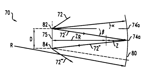
In FIGS. 3(a) and 3(b), a cross-sectional view of an optical switching
device 70 employing the principles of the present invention is illustrated.
Optical
switching device 70 includes an array of minors 75 and a curved concave
CA 02325611 2000-11-09
Giles 60-5 8
reflective component 80. In one embodiment, reflective component 80 is a
spherically shaped minor having a radius of curvature. In the alternative, a
parabolic or conic shaped mirror may also be employed as curved reflective
component 80.
Mirror array 75 is spaced from curved reflective component 80 by an
extended distance than the Rayleigh range, ZR, in comparison with optical
device 40
of FIG. 2(a). Array 75 and reflective component 80 are separated by a distance
equal to the sum of the Rayleigh range, ZR, and a displacement distance, Z.
The
increased separation between array 75 and reflective component 80 does not
scatter
optical signals being reflected between the mirrors of array 75 and reflective
component 80. The optical signals do not scatter because of the curvature of
diverging optical signal is equal to a curvature of reflective component 80.
Therefore, the radius of curvature of reflective component 80 corresponds with
displacement distance, Z, and the Rayleigh range, ZR, and this relationship
may be
1 S expressed by the following mathematical equation:
R=Z+ZRZ
Z
where R is the radius of curvature. It should be apparent to skilled artisans
from this
mathematical expression that the displacement distance, Z, created by curved
reflective component 80 increases as the radius, R, increases, for a given
Rayleigh
range, ZR. In one embodiment of the present invention, the optical signals
emanate
from a source having a width of approximately 0.5 mm such that the Rayleigh
range, ZR, is approximately 50 mm, the displacement distance, Z, is
approximately
20.7 mm, and the radius of curvature, R, is approximately 141.5 mm.
Each mirror in array 75 requires a smaller range than the steering range, ~,
of each mirror of array 55 of FIG. 2(a). The range of each mirror in array 75
is
smaller as a result of the additional spacing between array 75 and curved
reflective
component 80 caused by displacement distance Z. The range of each mirror in
CA 02325611 2000-11-09
Giles 60-5 9
array 75 is equal to the sum of half of an incoming angle, ,Q, and half of an
outgoing
angle, a. It should be apparent to skilled artisans, from laws of reflection
and
geometric optics, that to reflect or redirect an optical signal within an
angular range,
a mirror need tilt half the angle of the desired angular range. See O'Shea. As
shown in FIG. 3(b), the range of each mirror in array 75 is equal to the sum
of the
tilt required for each mirror to receive an incoming optical signal, ~2, and
the tilt
required for each mirror to direct an outgoing optical signal, a/2.
Incoming angle, ,Q, is the angle for which each mirror in array 75 is required
for an optical signal to be directed from one end of array 75 to the other end
of array
75. For the purposes of illustration, incoming angle, ~3, allows an optical
signal to
be directed from a first exemplary mirror 82 to a second exemplary mirror 84.
Incoming angle, ~, may be mathematically expressed by the following equation:
_ , D
(2ZR +2Z)
where D is the width of array 75. From the above mathematical equation,
incoming
angle, Vii, is inversely proportional to displacement distance, Z, such that
as
displacement distance, Z, increases, incoming angle, ~3, decreases, and vice
versa.
In one embodiment of the present invention, the width, D, of array 75 is
approximately 18.4 mm, and the incoming angle, ~3, is approximately 3.75
degrees.
Outgoing angle, c~ is the angle required for each mirror in array 75 to be
positioned to receive an outgoing optical signal from curved reflective
component
80. Outgoing angle, a, may be expressed by the following mathematical
equation:
D*Z
a = tan- ( 2 )
2ZR - ZR * Z
wherein outgoing angle, c~ is formed by the existence of displacement
distance. It
should be apparent to skilled artisans that that outgoing angle, c~ is
directly
CA 02325611 2000-11-09
Giles 60-5 10
proportional to displacement distance, Z, such that as displacement distance,
Z,
increases, reflective angular deviation, c~ increases, and vice versa. In one
embodiment of the present invention, the width, D, of array 75 is
approximately
18.4 mm, and the outgoing angle, c~ is approximately 3.75 degrees.
It should be also noted that by tilting clockwise to an angle of a/2, first
exemplary minor 82 is displaced from its neutral position by a distance ya.
Mirror
82 is also displaced from its neutral position by a distance y~ when tilted
counterclockwise to an angle of ,C~Y'2. As stated hereinabove, mirror 82 tilts
in
response to a voltage from a received control signal. The distances traveled,
ya or
y~, by mirror 82 each correspond with the voltage of the received control
signal.
Hence, a voltage of approximately 130V from a received control signal may be
required to cause mirror 82 to travel the distance ya or y~. In one
embodiment,
incoming angle, X13, and outgoing angle, a, are both equal to approximately
3.75
degrees, and the distances, ya and y~, are both equal to approximately 16.4
wm.
The following is a representation of the interaction between mirror array 75
and curved reflective component 80 in routing an incoming optical signal 72
through optical switching device 70 via outgoing optical signal 72"'. Upon
receiving a control signal, a first exemplary mirror 82 in array 75 is
positioned to
receive and reflect an incoming optical signal 72. First exemplary mirror 82
directs
optical signal 72' onto curved reflective component 80. Optical signal 72' is
directed by exemplary mirror 82 within a range of locations, 74a to 74a', on
curved
reflective component 80. Curved reflective component 80 receives the directed
optical signal 72' from exemplary mirror 82 at an incident angle with respect
to a
normal to a surface of curved reflective component 80. Employing the law of
reflection, an optical signal 72" is reflected off curved reflective component
80 at
an angle equal to angle of incidence. Optical signal 72" is directed back
towards a
location on array 75. In the present example, location 74a on curved
reflective
component 80 causes the optical signal 72" to be directed towards a second
exemplary mirror 84. Second exemplary mirror 84 is positioned, in response to
a
CA 02325611 2000-11-09
Giles 60-5 I I
control signal, to receive and reflect optical signal 72". Upon receiving
reflect
optical signal 72", second exemplary mirror 79 reflects an optical signal
72"'.
Thus, by positioning both first and second exemplary minors, 82 and 84, of
array
75, optical switching device 70 routes incoming optical signal 72 to outgoing
optical
signal 72"'. It should be apparent to skilled artisans in view disclosure
herein that a
plurality of optical signals may be routed using a multitude of mirrors on
minor
array 75 and curved reflective component 80.
Refernng to FIG. 4, a cross sectional view of an optical device 100 for
routing optical signals is illustrated employing the principles of optical
device 70 of
FIGS. 3(a) and 3(b). Optical device 100 routes a plurality of optical signals
from a
first portion of an input/output port 110 to a section portion of input/output
port 110.
In the present configuration, the first and second portions of input/output
port 110
are configured within a singular housing. It should be apparent to skilled
artisans
from the disclosure hereinbelow, however, that the alternate configurations
may also
be employed.
Each optical signal of the plurality of optical signals is routed using an
array
of mirrors 120 in combination with a curved concave reflective component 130.
Mirror array 120 is spaced from port 110 by a Rayleigh range. Mirror array 120
has
a matrix of reflective elements. In one embodiment, the matrix of reflective
elements is realized by a MEMS based mirror array. Each mirror of array 120
tilts
to a position in response to a control signal. Once an exemplary mirror of
array 120
is tilted to a specific position, the exemplary mirror may direct an incoming
optical
signal, using the law of reflection, to a particular location on curved
reflective
component 130. For the purposes of illustration, mirror array 120 includes a
first
and a second exemplary mirror, 125 and 135, respectively.
Reflective component 130 has a curved concave shape. The curvature of
reflective component 130 enables an increase in the spacing between array 120
and
component 130 to the sum of the Rayleigh range, ZR, and a displacement
distance,
Z, without scattering the optical energy being reflected between the mirrors
of array
120 and component 130. The optical signal does not scatter because of the
CA 02325611 2000-11-09
Giles 60-5 12
curvature of diverging optical signals matches the curvature of component 130.
The
Rayleigh range, ZR, displacement distance, Z, and radius of curvature, R,
mathematically correlate to one another, as expressed in the mathematical
equations
detailed hereinabove. In one embodiment of the present invention, curved
reflective
component 130 is a spherically shaped mirror. Various alternatives, however,
will
become apparent to skilled artisans upon reviewing the present disclosure.
The following is a representation of the interaction between mirror array 120
and curved reflective component 130 in routing an incoming optical signal 115
from
a first portion of input/output port 110 to a second portion of input/output
port 110.
Upon receiving a control signal, a first exemplary mirror 125 in array 120 is
positioned to receive and reflect incoming optical signal 115. First exemplary
minor 125 directs optical signal 115' onto curved reflective component 130.
Optical signal 115' is directed by exemplary mirror 125 within a range of
locations,
117a to 117a', on curved reflective component 130. Curved reflective component
130 receives the directed optical signal 115' from exemplary mirror 125 at an
incident angle with respect to a normal to a surface of curved reflective
component
130. Employing the law of reflection, an optical signal 115" is reflected off
curved
reflective component 130 at an angle equal to angle of incidence. Optical
signal
115" is directed back towards a location on array 120. In the present example,
location 117a on curved reflective component 130 causes the optical signal
115" to
be directed towards a second exemplary mirror 135. Second exemplary mirror 135
is positioned, in response to a control signal,, to receive and reflect
optical signal
115". Upon receiving optical signal 115", second exemplary minor 135 reflects
an
optical signal 115"'. Thus, by positioning both first and second exemplary
mirrors,
125 and 135, of array 120, optical switching device 100 routes incoming
optical
signal 115 from a first portion of input/output port 110 to a second portion
of
input/output port 110. It should be apparent to skilled artisans in view
disclosure
herein that a plurality of optical signals may be routed using a multitude of
mirrors
on mirror array 120 and curved reflective component 130.
Each mirror in array 120, including exemplary mirrors 125 and 135, requires
CA 02325611 2003-02-26
13
a smaller range than the steering range, ~, of each mirror of array 55 of FIG.
2(a).
The range of each mirror in array 120 is smaller as a result of the additional
spacing
between array 120 and curved reflective component 130 caused by displacement
distance Z. The range of each minor in array 120 is equal to the sum of the
tilt
required for each mirror to receive an incoming optical signal, ,EY2, and the
tilt
required for each mirror to direct an outgoing optical signal, crl2. By
tilting
clockwise to an angle of a/2 and counterclockwise to an angle of ~Y2, each
mirror
on array 120 travels from its neutral position by a particular travel
distance.
In one embodiment of the present invention, the optical signals emanate
from port 110 having a width of approximately 0.5 mm and wavelength of
approximately 1550 nm, such that the Rayleigh range, ZR, a Rayleigh range, ZR,
of
approximately 50 mm, a displacement distance, Z, of approximately 20.7 mm,
curved reflective component 130 has a radius of curvature, R, of approximately
141.5 mm, a width, D, of array 120 of approximately 18.4 mm, and incoming and
I 5 outgoing angles, ~B and c~ each equal to approximately 3.75 degrees. If
incoming
and outgoing angles, ,B and c~ are each equal to approximately 3.75 degrees,
each
mirror travels approximately 16.4 ~m when tilting clockwise and tilting
counterclockwise.
Referring to FIGS. 5(a) through 5(d), cross sectional views of several
~bodiments of a curved reflective component are illustrated. Each of these
realizations may be employed with a mirror array to extend the distance
between a
mirror array and the curved reflective component beyond the Rayleigh range
without scattering an optical signal. These embodiments include a convex lens
coupled to a planar mirror in FIG. 5(a), a planar mirror having a bi-convex
lens for
producing a converging reflected optical signal in FIG. 5(b), a Margin mirror
in
FIG. 5(c), and a compound Margin mirror in FIG. 5(d). For more information on
lens and mirror design, generally, and Margin mirrors particularly, see Smith,
"Modern Lens Design: A Resource Manual," McGraw-Hill 1992 (hereinafter
"Smith"). It should be apparent to one of ordinary skill that the examples
CA 02325611 2000-11-09
Giles 60-5 14
illustrated in FIGS. 5(a) through 5(d) are merely illustrative and not
exhaustive.
When employed in an optical device for routing signals as detailed herein
without
scattering optical signals, each of the curved reflective components, depicted
FIGS.
5(a) through 5(d), are spaced from a mirror array at a distance that
corresponds with
the radius of curvature of the particularly selected curved reflective
component - the
relationship between radius of curvature, R, Rayleigh range, ZR, and
displacement
distance, Z, is expressed in the mathematical equation detailed hereinabove.
Referring to FIG. 6, a cross sectional view of an optical device 150 for
routing optical signals is illustrated. Optical device 150 routes a plurality
of optical
signals from a first port 160 to a second port 200. First and second ports,
160 and
200, are not co-located in the present embodiment, unlike inputloutput port
110 of
FIG. 4.
Optical switch 150 includes a first and a second mirror array, 170 and 190,
in combination with a curved reflective component 180. Each mirror array has a
matrix of reflective elements or mirrors. First and/or second mirror array,
170
and/or 190, may be realized by a MEMS based mirror array formed on a common
substrate. Each of the mirrors of arrays, 170 and 190, may tilt in response to
a
control signal. Once the mirrors of the array 170 are positioned, one or more
incoming optical signals from first port 160 might be directed by the law of
reflection to a particular locations) on curved reflective component 180.
Curved reflective component 180 has a concave shape. The curvature of
component 180 enables an increase in the spacing between array 170 and
reflective
component 180, as well as the spacing between array 190 and reflective
component
180, to the sum of the Rayleigh range, ZR, and a displacement distance, Z,
without
scattering the optical energy being reflected between the mirrors of array 170
and
reflective component 180, and between the mirrors of array 190 and reflective
component 180. In one embodiment of the present invention, curved reflective
component 180 is a spherically shaped mirror. Various alternatives, however,
will
become apparent to skilled artisans upon reviewing the present disclosure.
The following is a representation of the interaction between mirror array
CA 02325611 2000-11-09
Giles 60-5 15
170, curved reflective component 180, and mirror array 190 in routing a pair
of
incoming optical signals 165 and 175 from first port 160 to a second port 200.
Upon receiving a control signal, a first and a second exemplary mirror, 205
and 210,
each are positioned to receive and reflect incoming optical signals 165 and
175.
First exemplary mirror 205 directs optical signal 165' onto curved reflective
component 180, while second exemplary mirror 210 directs optical signal 175'
onto
curved reflective component 180. Optical signal 165' is directed by exemplary
mirror 205 within a range of locations, 230a to 230a', on curved reflective
component 180. Likewise, optical signal 175' is directed by exemplary minor
210
within a range of locations, 230a to 230a", on curved reflective component
180.
Curved reflective component 180 receives directed optical signal 165' from
exemplary minor 205 at an incident angle with respect to normal to a surface
of
curved reflective component 180. Optical signal 175' is received by curved
reflective component 180 from exemplary mirror 210 at an incident angle with
respect to normal to a surface of curved reflective component 180. Employing
the
law of reflection, optical signals 165" and 175" are each reflected off curved
reflective component 180 at angles equal to their angles of incidence. In
turn,
optical signal 165" is directed towards a first location on second array 190,
while
optical signal 175" is directed towards a second location on second array 190.
In
the present example, location 230a' on curved reflective component 180 causes
optical signal 165" to be directed towards a third exemplary mirror 215 on
second
array 190, while location 230a" on curved reflective component 180 causes
optical
signal 175" to be directed towards a fourth exemplary minor 220 on second
array
190. Third exemplary mirror 215 is positioned, in response to a control
signal, to
receive and reflect optical signal 165". Fourth exemplary mirror 220 is
positioned,
in response to a control signal, to receive and reflect optical signal 175".
Upon
receiving optical signals 165" and 175", third and fourth exemplary mirrors,
215
and 220, reflect optical signals 165"' and 175"'. Thus, by positioning both
third
and fourth exemplary minors, 215 and 220, of array 190, optical switching
device
150 routes incoming optical signals 165 and 175 from first port 160 to second
port
CA 02325611 2000-11-09
Giles 60-5 16
160. It should be apparent to skilled artisans in view disclosure herein that
a
plurality of optical signals may be routed using a multitude of mirrors on
mirror
arrays 170 and 190 and curved reflective component 180.
Refernng to FIG. 7, a cross sectional view of an optical device 300 for
routing optical signals is illustrated. Optical device 300 routes a plurality
of optical
signals from a first port 310 to a second port 350. In one embodiment of the
present
invention, optical signals are directed from first port 310 to second port
350. In
alternative embodiment, a number of optical signals may be directed from a
first
portion of first port 310 to a first portion of second port 350, while other
optical
signals may be directed from a second portion of second port 350 to a second
portion of second port 310, such that port 310 directs and receives optical
signals
from port 350 and port 350 directs and receives optical signals from port 310.
Optical switch 300 includes a first and a second mirror array, 320 and 340,
in combination with an optical component 330. Each mirror array, 320 and 340,
has
a matrix of reflective elements or mirrors. First and/or second mirror array,
320
and/or 340, may be realized by a MEMS based mirror array. Optical component
330 is realized by a bi-convex optical lens. Various alternatives, however,
will
become apparent to skilled artisans upon reviewing the present disclosure.
Each of
the mirrors of arrays, 320 and 340, may tilt in response to a control signal.
Once the
mirrors of the array 320 are positioned, at least one incoming optical signal
from
first port 310 might be directed by the law of reflection to the array 340,
through bi-
convex optical lens 330, and thereafter second port 350.
Bi-convex optical lens 330 has converging properties. The converging
properties enable an increase in the spacing between array 320 and optical
lens 330,
as well as the spacing between array 340 and optical lens 330, to the sum of
the
Rayleigh range, ZR, and a displacement distance, Z. The increase in separation
however does not scatter the optical energy being reflected between the minors
of
array 320 and optical lens 330, and between the mirrors of array 340 and
optical
lens 330.
The following is a representation of the interaction between first mirror
array
CA 02325611 2000-11-09
Giles 60-5 17
320, bi-convex optical lens 330, and second mirror array 340 in routing a pair
of
incoming optical signals 315 and 325 from first port 310 to a second port 350.
Upon receiving a control signal, a first and a second exemplary minor, 355 and
360,
each are positioned to receive and reflect incoming optical signals 315 and
325.
First exemplary minor 355 directs optical signal 315 within the range of 315a'
and
315b' towards bi-convex optical lens 330 depending on the position of first
exemplary mirror 355. Likewise, second exemplary mirror 360 directs optical
signal 325 within the range of 325a' and 325b' towards bi-convex optical lens
330
depending on the position of second exemplary mirror 360.
Bi-convex optical lens 330 directs optical signals reflected from first and
second exemplary mirrors, 355 and 360, towards second mirror array 340. With
respect to first exemplary mirror 355, if optical signal 315 takes the 315a'
path, lens
330 forms optical signal 315a". As a result, optical signal 315a" is directed
by
lens 330 towards a third exemplary mirror 365 on mirror array 340. Exemplary
minor 365 receives optical signal 315a" and forms a reflected optical signal
345
directed toward a first portion of port 350. In the alternative, if optical
signal optical
signal 315 takes the path 315b', lens 330 forms optical signal 315b", which is
directed towards a fourth exemplary mirror 370 on mirror array 340. Exemplary
minor 370 receives optical signal 315b" and forms a reflected optical signal
335
directed toward a second portion of port 350. With respect to second exemplary
minors 360, if optical signal 325 takes the 325a' path, lens 330 forms optical
signal
325a". As a result, optical signal 325a" is directed by lens 330 towards
fourth
exemplary mirror 370. Exemplary minor 370 receives optical signal 325a" and
forms reflected signal 335 directed toward the second portion of port 350.
Alternatively, lens 330 forms optical signal 325b" if the optical signal takes
the
path 325b'. Optical signal 325b" is directed towards third exemplary mirror
365.
Exemplary mirror 365 receives optical signal 325b" and forms a reflected
optical
signal 345 directed toward the first portion of port 350. It should be
apparent to
skilled artisans in view disclosure herein that a plurality of optical signals
may be
routed using a multitude of mirrors on mirror arrays 320 and 340 and bi-convex
lens
CA 02325611 2000-11-09
Giles 60-5 18
component 330.
Referring to FIGS. 8(a) and 8(b), a cross sectional view of an optical
switching device 400 for routing optical signals is illustrated. Optical
device 400
routes a plurality of optical signals between a first and a second port, 410
and 450.
More particularly, device 400 routes optical signals from a first portion of a
first
port 410 to a first portion of a second port 450, a second portion of second
port 450
to a second portion of first port 410. Device 400 also routes optical signals
from a
third portion from first port 410 to a fourth portion of first port 410, and a
third
portion from second port 450 to a fourth portion of first port 450.
Optical switch 400 includes a first and a second mirror array, 420 and 440,
in combination with an optical component 430. Each mirror array, 420 and 440,
has
a matrix of reflective elements or minors. First and/or second mirror array,
420
and/or 440, may be realized by a MEMS based mirror array. Optical component
430 includes a bi-convex optical lens having a two-sided patterned mirror 435
embedded therein. As illustrated in FIG. 8(b), patterned mirror 435 has a
checkerboard configuration including non-reflective, lens portions 436
alternating
with reflective, mirror portions 438. Reflective, mirror portions 438 are
reflective
on both sides such that an exemplary optical signal emanating from array 420
may
be reflected back towards array 420, while an exemplary optical signal
emanating
from array 440 may be reflected back towards array 440. The dimensions of lens
portions 436 and reflective, mirror portions 438, are advantageously at least
equal to
the dimensions of an optical beam as it approaches portions 436 or 438 of
patterned
mirror 435. In one embodiment, non-reflective, lens portions 436 and
reflective,
mirror portions 438 each have a dimension of 0.5 mm by 0.5 mm.
Bi-convex optical lens 430 has converging properties. The converging
properties enable an increase in the spacing between array 420 and optical
lens 430,
as well as the spacing between array 440 and optical lens 430, to the sum of
the
Rayleigh range, ZR, and a displacement distance, Z. The increase in separation
however does not scatter the optical energy being reflected between the minors
of
array 420 and optical lens 430, and between the mirrors of array 440 and
optical
CA 02325611 2000-11-09
Giles 60-5 19
lens 430.
The following is a representation of the interaction between first mirror
array
420, bi-convex optical lens 430, and second mirror array 440 in routing
optical
signals 415 and 455. It should be apparent to skilled artisans in view
disclosure
herein, however, that a plurality of optical signals may be routed using a
multitude
of mirrors on mirror arrays 420 and 440 and lens 430. Upon receiving a control
signal, a first exemplary mirror 475 of mirror array 420 is positioned to
receive and
reflect optical signal 415. First exemplary mirror 475 directs optical signal
415
within a range of 415a' and 415b' towards bi-convex optical lens 430,
depending on
the position of first exemplary mirror 475. If optical signal 415 takes the
415a'
path, optical signal 415a' passes through a non-reflective, lens portion 436
of bi-
convex optical lens 430 to form optical signal 415a". As a result, optical
signal
415a" is directed by lens 430 towards a second exemplary mirror 495 of array
440.
Exemplary mirror 495 receives optical signal 415a" and, in response to a
control
1 S signal, is positioned to form a reflected optical signal 445 directed
towards a first
portion of port 450. Alternatively, if optical signal 415 takes the 415b'
path, optical
signal 415b' is reflected off a minor portion 438 of lens 430 to form optical
signal
415b". As a result, optical signal 415b" is directed by the minor portion 438
of
lens 430 towards a third exemplary mirror 480 of array 420. Exemplary mirror
480
receives optical signal 415b" and, in response to a control signal, is
positioned to
form a reflected optical signal 425 directed towards a second portion of port
410.
Similarly, upon receiving a control signal, a fourth exemplary mirror 500 of
mirror array 440 is positioned to receive and reflect optical signal 455.
Exemplary
minor 500 directs optical signal 455 within a range of 455a' and 455b' towards
bi
convex optical lens 430, depending on the position of first exemplary mirror
500. If
optical signal 455 takes the 455a' path, optical signal 455a' passes through a
non-
reflective, lens portion 436 of bi-convex optical lens 430 to form optical
signal
455a". As a result, optical signal 455a" is directed by lens 430 towards third
exemplary mirror 480 of array 420. Exemplary mirror 480 receives optical
signal
455a" and, in response to a control signal, is positioned to form a reflected
optical
CA 02325611 2000-11-09
Giles 60-5 20
signal 425 directed towards a second portion of port 410. Alternatively, if
optical
signal 455 takes the 455b' path, optical signal 455b' is reflected off a
mirror portion
438 of lens 430 to form optical signal 455b". As a result, optical signal
455b" is
directed by the mirror portion 438 of lens 430 towards second exemplary minor
495 of array 440. Exemplary mirror 495 receives optical signal 455b" and, in
response to a control signal, is positioned to form a reflected optical signal
445
directed towards a second portion of port 450.
While the particular invention has been described with reference to
illustrative embodiments, this description is not meant to be construed in a
limiting
sense. It is understood that although the present invention has been
described,
various modifications of the illustrative embodiments, as well as additional
embodiments of the invention, will be apparent to one of ordinary skill in the
art
upon reference to this description without departing from the spirit of the
invention,
as recited in the claims appended hereto. Thus, while detailed the present
invention
applies to an optical switch for routing optical signals between an input and
output
port, it should be apparent to one of ordinary skill that the present
invention may
also be applied to any apparatus for beam steering electromagnetic energy,
including, for example, liquid crystal devices. It is therefore contemplated
that the
appended claims will cover any such modifications or embodiments as fall
within
the true scope of the invention.