Note: Descriptions are shown in the official language in which they were submitted.
CA 02333731 2000-11-30
WO 00/58315 PCT/KROO/00289
ORGANOMETALLIC COMPLEX MOLECULE AND ORGANIC
ELECTROLUMINESCENT DEVICE USING THE SAME
BACKGROUND OF THE INVENTION
The present invention generally relates to organic electroluminescence.
More particularly, the present invention pertains to an organometaflic complex
molecule and an organic electroluminescent (hereinafter referred to as
"organic
EL") device using the organometallic complex molecule.
Organic electroluminescence is one of the instances, in which electric
current is directly converted into visible light by internal processes of
organic
fluorescent or light-emitting molecules. In recent years, great attention has
been given to the improvement of organic EL technology since it can be used in
a new type of flat panel display, which can replace the liquid crystal display
(LCD) technology. Individual colors of red, green or blue can be emitted, or
they can be combined to create full color image display. This technology is
advantageous over LCD technology in its low power consumption, faster
response time, higher brightness level, unlimited viewing angle and thinner
design.
A basic construction of an organic EL device includes two opposing
electrodes, i.e., a cathode and an anode, and an intervening layer containing
an
organic light-emitting or fluorescent material. When applying an electric
voltage
between the electrodes, electrons and holes are injected from the cathode and
the anode, respectively, into the intervening layer and recombined therein.
Recombined pairs of electrons and holes, namely excitons, move around
carrying the energy generated by the recombination and transfer the energy to
the organic fluorescent molecules. The transferred energy excites valence
electrons of the organic fluorescent molecules and generate photons when the
electrons return to their ground state.
CA 02333731 2000-11-30
WO 00/58315 PCT/KROO/00289
2
In order to improve energy efficiency, multiple-layered organic EL devices
have been suggested. Generally, multiple-layered organic EL devices have one
or more of hole-injecting layer, hole-transporting layer, light-emitting layer
electron-transporting layer, and electron-injecting layer. The carrier
(electron or
hole) injecting layer or carrier transporting layer may work as a light
emitting
layer as well when organic fluorescent materials are doped therein. Organic EL
devices having multiple layers are expensive to manufacture due to the
significant accompanying processing. Thus, it is desirable that one layer of
the
organic EL device has multiple functions: e.g., one for electron-
injection/transportation as well as light-emission.
In order to improve luminescence efficiency of a light-emitting layer,
another light-emitting material having a higher quantum yield is doped in the
light-emitting layer. Excitons are known to have a tendency to transfer their
energy to a material having a smaller band gap among materials near the
recombination location. Accordingly, a dopant is selected from materials
having
a high quantum yield and a smaller band gap (larger wavelength) than the host
material; otherwise, the excitons' energy will be transferred the host
material
having a lower quantum yield, accordingly generating weak or no emission.
Tris (8-hydroxyquinoline) aluminum complex (Alq3) is known as a
material having light-emitting and electron-injection/transportation
properties.
A1q3 has a band gap for green light emission. A light-emitting material to be
doped in an Alq3 layer needs to have a larger wavelength than the green light
of the AIq3. Accordingly, blue light-emitting materials may not be doped in an
AIq3 layer. DPVBi and B-Alq emitting blue light can be used as an electron-
transporting material as well. However, these materials require a high driving
voltage when directly contacting with the cathode because of their high
reduction potentials. In order to use these materials in a light-emitting
layer
CA 02333731 2000-11-30
WO 00/58315 PCT/KROO/00289
3
functioning the electron-transporting as well, a separate electron-injection
layer
is needed.
Thus, there is a need for a new material, which can host a light-emitting
material for blue light emission with a low reduction potential. Also, there
are
other needs to introduce a new material for use in an organic EL device.
SUMMARY OF THE INVENTION
One aspect of the present invention provides an organometallic complex
for use in organic EL devices. The complex compounds have a structure
satisfying the following Chemical Formula (1):
A
N ~ X
Chemical Formula (1) M
0 0
z
B
n
In the Chemical Formula (1), "X" is one selected from the group
consisting of carbon, oxygen, sulfur, selenium, and nitrogen with an alkyl or
aromatic functional group. "Z" is one selected from the group consisting of
oxygen, sulfur, and nitrogen with an alkyl or aromatic functional group. "M"
represents a metal and preferably is a monovalent, divalent or trivalent
metal.
"n" is a positive integer depending upon the oxidation state of the metal "M".
"A"
and "B" are an aromatic or heterocyclic ring.
Another aspect of the present invention provides a light-emitting
composition, which comprises an organometallic complex having a structure
satisfying Chemical Formula (1).
CA 02333731 2000-11-30
WO 00/58315 PCT/KR00/00289
4
Another aspect of the present invention provides an electron-transporting
composition, which comprises an organometallic complex having a structure
satisfying Chemical Formula (1).
Another aspect of the present invention provides an organic EL device,
which comprises a a first electrode, a second electrode opposing the first
electrode, and a first layer located between the first electrode and the
second
electrode. The first layer contains an organometallic complex having a
structure
satisfying Chemical Formula (1).
Still another aspect of the present invention provides an electronic device,
which comprises a organic EL device display, making use of an organometallic
complex.
Still another aspect of the present invention provides a method of
generating visible light from an electronic device. The method comprises
injecting electrons and holes from two opposing electrodes into at least one
layer located between the two electrodes by applying electric power to the two
electrode. The at least one layer contains an organometallic complex
satisfying
Chemical Formula (1).
Still another aspect of the present invention provides a method of
manufacturing an organic EL device. The method comprises providing a
substrate, forming a first conductive layer, forming at least one layer; and
forming a second conductive layer. The at least one layer contains an
organometallic complex of Chemical Formula (1).
BRIEF DESCRIPTION OF THE DRAWINGS
Figure 1 illustrates a cross-sectional view of an organic EL device in
15 accordance with one exemplary embodiment of the present invention.
Figure 2 illustrates a cross-sectional view of an organic EL device in
accordance with another embodiment of the present invention.
CA 02333731 2000-11-30
WO 00/58315 PCT/KROO/00289
Figure 3 illustrates a cross-sectional view of an organic EL device in
accordance with another embodiment of the present invention.
Figure 4 is a UV-visible absorption spectrum and a light emitting
spectrum discussed in Example 4.
5 Figure 5 illustrate current and driving voltage of the organic EL device of
Example 5.
Figure 6 is a light emitting spectrum of the organic EL device of Example
6.
Figure 7 is a light emitting spectrum of the organic EL device of Example
7.
DETAILED DESCRIPTION OF EMBODIMENTS OF THE INVENTION
Now the various aspects of the present invention will be discussed in
more detail. It is to be understood at the outset of the description, which
follows
that persons of skill in the appropriate arts may modify the invention here
described while still achieving the favorable results of this invention.
Accordingly,
the following description is to be understood as being a broad, teaching
disclosure directed to persons of skill in the appropriate arts, and not as
limiting
upon the present invention.
New Organometallic Complex Compounds
New organometallic complex compounds have been synthesized and
researched by the present inventors. These organometallic complex materials
have various properties for use in organic EL devices.
The new organometallic complex compounds are represented by the
following Chemical Formula (1):
CA 02333731 2000-11-30
WO 00/58315 PCT/KROO/00289
6
A
.N ~ X
M '
Chemical Formula (1) 0 0
Z
e9n
In the Chemical Formula (1), "X" is one selected from the group
consisting of carbon, oxygen, sulfur, selenium, and nitrogen with an alkyl or
aromatic functional group.
"Z" is one selected from the group consisting of oxygen, sulfur, and
nitrogen substituted with an alkyl or an aromatic group, in which hydrogens of
an aromatic functional group can be substituted with alkyl, aromatic, halogen,
amine group, etc.
"M" represents a metal and preferably is a monovalent, divalent or
trivalent metal. More preferably, "M" is one selected from lithium,
berylliurn, zinc,
magnesium, gallium, indium and aluminum. Most preferably, "M" is lithium, or
zinc.
"n" is a positive integer depending upon the oxidation state of the metal
"A" is an aromatic or heterocyclic ring, in which hydrogens of the ring
can be substituted with alkyl, aromatic, halogen, amine group, etc.
Preferably,
ring "A" is one selected from the group consisting of the rings as shown
below,
which are shown together with the pentagonal ring having N and "X".
CA 02333731 2000-11-30
WO 00/58315 PCT/KROO/00289
7
OO0>-
ooo}- N
N
O o
O r C O O o
N~ N
~
N x X X
>-- Yac > -- >-
ON N N @~N
X
O o}- o ~>-
s N
"B" is an aromatic or heterocyclic ring, in which hydrogens of the ring can be
substituted with alkyl, aromatic, halogen, amine group, etc. Preferably, ring
"B"
is one selected from the group consisting of the rings as shown below, which
are shown together with the hexagonal ring with "Z".
CA 02333731 2000-11-30
WO 00/58315 PCT/KROO/00289
8
\
\p o \o
z
z z
oVj o 0
\p \p
z
ooZ Z oZ
CH3
\p \p t(~
z o o z N
00
\p \p \p
Z
N
oN Z "oZ
Following Chemical Formulas (2) to (12) are organometallic complexes
satisfying the general structure of Chemical Formula (1). These organometallic
complex compounds are listed to provide examples of Chemical Formula (1)
only and do not limit the scope of the organometallic complex according to the
present invention.
CA 02333731 2000-11-30
WO 00/58315 PCT/KROO/00289
9
0
Chemical S
Zn Chemical
Zn 5 Formula (2) 0 Formula (3)
0 o o
2
=
,-N S O
Chemical Be ee Chemical
Formula (4) ~ Formula (5)
o
0 0
2 2
0 0
N 0
Chemical Zn - ' ' Zn . '' Chemical
Formula (6) o Formula (7)
N-ph N-ph
0 0
2 2
p ,25 Chemical Be Be -" Chemical
Formula (8) Formula (9)
N-ph N-ph
0 0
2 2
CA 02333731 2000-11-30
WO 00/58315 PCT/KROO/00289
p
Chemical N S ,N o Chemical
Formula (10)Z' o o Zn o o Formula(11)
5 N-CH3 N-CH3
0 0
2 2
=
O
10 Chemical Be - o 0
Formula (12)
N-CHs
0
2
The new organometallic complex compounds satisfying Chemical
Formula (1) in accordance with the present invention generally have a light-
emitting or fluorescent property, in particular, with a band gap for blue
emission.
A light-emitting layer of an organic EL device can be made of these
organometallic complex compounds. Also, these complex materials having a
light-emitting property can host other fluorescent or light-emitting materials
to
improve the efficiency and/or to tune various colors of light-emission. All
the
complex materials that have been synthesized by the inventors showed a light-
emitting property although some satisfying Chemical Formula (1) might not emit
light. The organometallic complex compounds having a band gap
corresponding to blue light emission, whether or not being fluorescent, can
host
other fluorescent materials for blue light emission or emission of light
having a
longer wavelength.
The new organometallic complex compounds of the present invention
generally have a good electron-transporting property. An electron-transporting
CA 02333731 2000-11-30
WO 00/58315 PCT/KROO/00289
11
layer of an organic EL device can be formed of these complex compounds. In
combination with the light-emitting property, these complex compounds may
form one layer functioning both light-emission and electron-transportation.
Also,
a low reduction potential of these materials of the present invention enables
to
avoid forming a separate electron-injecting layer.
Moreover, these new organometallic complex compounds
advantageously block holes transferred from a neighboring layer in an organic
EL device. This hole blocking property enables to selectively move the
emission zone between the two layers. If the neighboring layer, e.g., a hole-
transporting layer, is not doped with a fluorescent material, the light emits
at the
organometallic complex near the boundary of the two layers. In the
alternative,
if the hole-transporting layer is doped with a fluorescent material, emission
can
occur only at the doped neighboring layer since the holes may not easily cross
the boundary into the complex material layer.
A band gap, a highest occupied molecular orbital (HOMO) level and a
lowest unoccupied molecular orbital (LUMO) level of compounds satisfying
Chemical Formula (1) are adjustable with changes of metal "M", ring "A", ring
"B", and substituting hydrogen atoms of aromatic groups with alkyl, aromatic,
halogen, amine group, etc.
Furthermore, these compounds have relatively high melting points, which
will improve thermal stability of any electronic devices using the these
materials,
particularly, organic EL devices. The characteristics of the organometallic
complex compounds will be further discussed in terms of organic EL devices
using them.
Organic EL Devices
The present inventors have also developed organic EL devices, which
use organometallic complexes satisfying Chemical Formula (1). In the organic
CA 02333731 2000-11-30
WO 00/58315 PCT/KROO/00289
12
EL devices, these organometallic complexes are used as a material for electron-
transportation and/or light-emission although not limited thereto. Also,
depending upon the matching of the conduction band of a complex material of
Chemical Formula (1) with the work function of a cathode material, an electron-
transporting layer made of the complex material works as an electron-injection
layer as well. Moreover, these complex materials enable a single layer
construction for the electron-injection, electron-transportation, and light-
emission
with or without doping of appropriate fluorescent materials, particularly blue
emission.
Now some exemplary organic EL device constructions will be discussed
with reference to the accompanying drawings. Figures 1 to 4 illustrates
simplified cross-sectional views of laminated structures of the exemplary
organic
EL devices in accordance with the present invention. The organic EL devices
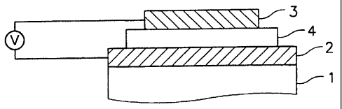
shown in Figures 1 to 4 commonly include a substrate 1, an anode 2 deposited
on the substrate, and a cathode 3 separated from the anode 2 by one or more
laminated layers. In these drawings, same reference numbers have been used
to indicate like components between the embodiments.
Figure 1 shows an exemplary organic EL device construction having a
single light-emitting layer 4 between the anode 2 and the cathode 3. When the
device is forward-biased between the anode 2 and the cathode 3, electrons and
holes are injected into the light-emitting layer 4 from the cathode 3 and the
anode 2, respectively. The light-emitting layer 4 contains an organometallic
complex compound of Chemical Formula (1) as a light-emitting material or light-
emitting host material.
As a light emitting material, an organometallic complex of Chemical
Formula (1) generates visible light when electrons and hole recombine in the
layer 4. Preferably, the light-emitting layer 4 is primarily made of an
organometallic complex compound of Chemical Formula (1). The complex
CA 02333731 2000-11-30
WO 00/58315 PCT/KROO/00289
13
compounds as a fight-emitting material can host another fluorescent or light-
emitting material as a dopant to improve the light-emission efficiency and/or
to
tune the color of light emission. Even if an organometallic complex of
Chemical
Formula (1) does not have a fluorescent property, the organometallic complex
may primarily form the light-emitting layer by hosting a light-emitting
dopant.
Advantageously, the dopant is distributed preferably near the anode 2. The
mobility of electrons in the light-emitting layer 4 is advantageously higher
than
that of the holes. Thus, the recombination of the holes and electrons takes
place at locations closer to the anode 2 than the cathode 3, where the dopants
are preferably present.
Referring to Figure 2, a hole-transporting layer 5 is provided on the
anode 2, and an electron-transporting layer 6 is located between the hole-
transporting layer 5 and the cathode 3. The electron-transporting layer 6
advantageously contains an organometallic complex material of Chemical
Formula (1). Preferably, the electron-transporting layer 6 of the organic EL
device is primarily made of an organometallic complex compound satisfying
Chemical Formula (1) as an electron-transporting material. In this
construction,
light-emission can occur in either or both of the hole-transporting layer 5
and the
electron-transporting layer 6 depending upon doping of light-emitting
materials.
If the organometallic complex material used in the electron-transporting
layer 6 has fluorescent characteristics, the electron-transporting layer 6 can
emit
visible light even without doping of another light-emitting material. In order
to
improve the light-emitting efficiency, however, it is preferable to dope
another
light-emitting material having higher fluorescent efficient in the electron-
transporting layer 6. In the alternative or in combination with the light-
emission
from the electron-transporting layer 6, the hole-transporting layer 5 can be
made
of or doped with a fluorescent material. In this case, visible light can be
emitted
from the hold-transporting layer 5 when electrons and holes recombine therein.
CA 02333731 2000-11-30
WO 00/58315 PCT/KROO/00289
14
When doping a fluorescent material in either or both of the hole-transporting
layer 5 and electron-transporting layer 6, preferably, the fluorescent
material is
doped near the boundary between the two layers 5 and 6.
Figure 3 shows another exemplary organic EL device construction, in
which a separate light-emitting layer 8 is sandwiched between a hole-
transporting layer 7 and an electron-transporting layer 9. In this
construction, an
organometallic complex compound satisfying Chemical Formula (1) is preferably
used in either or both of the light-emitting layer 8 and the electron-
transporting
layer 9.
When the light-emitting layer 8 contains an organometallic complex
compound satisfying Chemical Formula (1), the electron-transporting layer 9
can be made of the same or another organometallic complex satisfying
Chemical Formula (1), or any other appropriate electron-transporting
materials.
In the alternative, an organometallic complex compound satisfying Chemical
Formula (1) is used in the electron-transporting layer 9, the light-emitting
layer 8
may contain the same or another organometallic complex compound satisfying
Chemical Formula (1), or any other appropriate light-emitting materials. In
either of the cases, the light-emitting layer 9 may be doped with another
fluorescent material.
In the exemplary organic EL device constructions of the present invention
shown in Figures 1-3, the substrate 1 is advantageously made of a transparent
material to allow the visible light emitted by the device to pass through.
Materials, which can be used for the substrate 1, for example, include glass,
quartz and any other appropriate artificial materials such as plastics.
Preferably,
glass is used for the substrate 1.
The anode 2 is a conductive electrode electrically connected to an
electric power source. Advantageously, the anode 2 is also made of a
transparent material for the same reason as provided for the substrate 1. The
CA 02333731 2000-11-30
WO 00/58315 PCT/KROO/00289
anode 2 requires a relatively large work function, advantageously greater than
4
eV. For example, conductive materials which can be used for the anode 2
include: carbon; aluminum, vanadium, chromium, copper, zinc, silver, gold,
similar metals, and alloys of the foregoing metals; zinc oxide, indium oxide,
5 induim tin oxide (hereinafter referred to as "ITO"), indium zinc oxide and
similar
tin oxide or tin oxide indium-based complex compounds; mixtures of oxides and
metals, such as ZnO:Al, Sn02:Sb; and conductive polymers, such as poly (3-
methylthiophene), poly[3,4-(ethylene-1,2-dioxy)thiophene], polypyrrole, and
polyaniline. Preferably, the anode 2 is made of ITO. Although not illustrated,
10 the anode 2 may be constructed in multiple layers of materials. The
thickness
of the anode 2 may vary depending on the materials used and its layered
structures. However, the anode 2 is laminated advantageously in the range of
about 10 nm to about 1000 nm, preferably from about 10 nm to about 500 nm.
The cathode 3 requires a relatively small work function, advantageously
15 smaller than 4 eV. The cathode 3 may also be made of a transparent material
for the same reason as provided for the substrate 1. For example, conductive
materials which can be used for the cathode 3 include: magnesium, calcium
sodium, potassium, titanium, indium, yttrium, lithium, gadolinium, aluminum,
silver, tin, lead, and similar metals and alloys thereof. Preferably, the
cathode 3
is made of aluminum-lithium alloy. Although not illustrated, the cathode 3 may
be constructed in multiple layers of materials. For example, the cathode 3 is
bilayered, such as LiF/Al and Li2O/AI. The thickness of the anode 3 may vary
depending on the materials used and its layered structures. However, the
cathode 3 is laminated advantageously in the range of about 1 nm to about
10,000 nm, preferably from about 10 nm to about 5,000 nm.
The electron-transporting layer 6, 9 contains an electron-transfer material
to transfer the electron injected from the cathode 3 to a light-emitting layer
4, 8
or to an area where light-emitting materials are doped. Compounds having a
CA 02333731 2000-11-30
WO 00/58315 PCT/KR00/00289
16
high electron mobility is used as an electron-transporting material. The
electron-transporting layer 6, 9 also has the function of blocking holes from
the
anode 2 or the neighboring layer 5 move toward the cathode 3. The electron-
transporting layer 6, 9 is to enable a large number of electron to be injected
from the cathode 3 at a low electric field applied to the device. Although not
illustrated in the exemplary constructions of Figures 1-3, another layer for
electron-injection may be needed in addition to the electron-transportine
layer 6,
9. In such a construction, the electron-injection layer is advantageously
located
between the cathode 3 and the electron-transporting layer 6, 9. The LUMO
level of the electron-injecting layer is located between the work function of
the
cathode 3 and that of the electron-transporting layer 6, 9.
As discussed above, the electron-transporting layers 6, 9 are preferably
made of an organometallic complex compound of Chemical Formula (1). The
electron-transporting layers 6, 9 may further contain other electron-
transporting
materials along with the organometallic complex compounds satisfying
Chemical Formula (1). For example, aluminum complexes of 8-
hydroxyquinoline can be added.
The hole-transporting layer 5, 7 containing a hole-transfer material has
the function to smoothly transfer the holes injected from the anode 2 to a
light-
emitting layer 4, 8 or to an area where light-emitting materials are doped.
Materials having a high hole mobility therein is advantageous. This layer 5, 7
also has the function of blocking electrons from the cathode 3 or the
neighboring layer 6 to move toward the anode 2. Another important function of
the hole-transporting layer 5, 7 is to enable a large number of holes to be
injected from the anode 2 at a low electric field applied to the device.
Although
not illustrated, another layer for hole-injection may be needed in addition to
the
hole-transportine layer 5, 7. In this construction, the hole-injection layer
is
advantageously located between the anode 2 and the hole-transporting layer 5,
CA 02333731 2000-11-30
WO 00/58315 PCT/KR00/00289
17
7. The HOMO level of the hole-injecting layer is located between that of the
hole-transporting layer 5, 7 and the work function of the anode 2.
For example, hole-injecting materials include metal porphyrine and
derivatives of quinacridone. Examples of hole-transporting materials are
oxadiazole derivatives, triazole derivatives, phenylene derivatives, arylamine
derivatives, conjugated poylmers, block co-polymers with conjugated and non-
conjugated repeating units, and the like. Normally, hole-transporting
materials
function for both the hole-injection and hole-transportation without a
separate
hole-injecting layer. The hole transporting layer 5, 7 may contain one or more
of
these hole injecting/transporting materials. Advantagously, a derivative of
the
arylamine, 4,4'-bis[N-(1-naphthyl)-N-phenylamino]biphenyl(NPB) is used as the
material for the hole-transporting layers 5, 7.
The light-emitting layers 4, 8 can further include other appropriate
fluorescent material along with an organometallic complex material of Chemical
Formula (1). Such fluorescent materials include, for example, 8-
hydroxyquinoline metal complex, dimerized styryl compound (U.S Patent No.
5,366,811), BAlq (U.S. Patent No 5,150,006), 10-hydroxybenzo [h] quinoline-
metal complex (U.S. Patent No. 5,529,853), 2-(2'-hydroxy-5'methylphenyl)
benzotriazole metal complex (U.S. Patent No. 5,486,406), benzoxazole,
benzthiazole, benzimidazole and derivatives thereof (U.S. Patent No.
5,645,948), poly(p-phenylene vinylene) and derivatives thereof (Synthetic
Metals 91, 35, 1997 and Synthetic Metals 91, 109, 1997), spiro compound (U.S.
Patent No. 5,840,217), polyfluorene, rubrene or the like. These materials can
also be mixed with the organometallic complex compounds satisfying Chemical
Formula (1) with or without dopants. Although not illustrated, the light-
emitting
layer 4, 8 may include multi-sublayers of different light-emitting materials
emitting different colors in order to tune the color of the emission light.
Alternatively or in combination with the multi-sublayer configuration, these
light-
CA 02333731 2000-11-30
WO 00/58315 PCT/KROO/00289
18
emitting layer 4, 8 may include a layer containing a mixture of more than one
light-emitting material.
Fluorescent dopants are provided in one or more of the layers of an
organic EL device to improve the light-emission efficiency, to tune the color
of
the emission, and/or to simply emit light from a layer having a non-
fluorescent
host. A dopant is selected from fluorescent materials having a higher quantum
efficiency than the host material. Preferably, the dopants have a quantum
yield
close to "1" in a dilute system. For example, fluorescent materials, which can
be
used as a dopant in an organic EL device, include: perylene, rubrene,
coumarine, quinacridone, nile red, DCM, etc.
When fight-emitting materials are doped into any of the light-emitting,
hole-transporting and electron-transporting layers 4, 5, 6, 8, it is
preferable that
light-emitting materials having a band gap close to that of the host materials
are
selected. More preferably, light-emitting materials to be doped into the host
materials have a slightly smaller band gap than that of the host materials.
More
than one light-emitting materials can be doped together in a light-emitting
layer
4, 8, hole-transporting layer 5 or electron-transporting layer 6. Like the
multi-
sublayered light-emitting layer as discussed above, more than one different
dopants can be doped in multi-layered configuration in the host layer.
In either configuration whether or not a separate light-emitting layer is
provided, quantum efficiency and lifetime of the organic EL device can be
enhanced depending on the selection of light-emitting materials and their
concentrations. Also, the thickness of the sublayers and the concentrations of
the light-emitting materials can be adjusted to obtain a narrow emission
spectrum, meaning to fine tune the color.
Various aspects and features of the present invention will be further
discussed in terms of the following examples, which are intended to illustrate
the present invention but not limit the scope of the present invention.
CA 02333731 2000-11-30
WO 00/58315 PCT/KROO/00289
19
ORGANOMETALLIC COMPLEX
EXAMPLE 1: Synthesis of Chemical Formula (2)
Preparation of Ligand Precursor Chemical_Formula (13)
50 ml of dimethyl sulfoxide (DMSO) was charged into a vessel cleaned
with nitrogen. Next, 2.5 g of 4-hydroxycoumarine and 2.1 g of
phenylisothiocyannate were added to the DMSO and dissolved, thereby forming
a mixture. 1.55 g of triethylamine was added to the mixture and components in
the mixture were subjected to reaction while agitating at room temperature for
2
hours. After reaction was completed the reaction solution was added to 100 ml
of hydrogen chloride of 3 N concentration to form a yellow solid.
Subsequently,
the yellow solid was dried, and by recrystallizing the yellow solid in 200 ml
of
acetone, 2.4 g of a compound of Chemical Formula (13) below was obtained at
the yield of 52 percent.
CA 02333731 2000-11-30
WO 00/58315 PCT/KROO/00289
OH S
Chemical Formula (13) 0
NH
ao 0
5 Preparation of ogand Chemical Formula (14)
0.2 g of the compound represented by Chemical Formula (13) above
was dissolved in 10 ml of chloroform, then 0.034 ml of bromine was slowly
added to the chloroform solution and left to react at room temperature for 5
hours. A precipitate formed by the reaction was then filtered, washed with
10 ethanol, and dried in vacuum to obtain 0.18 g of a ligand compound of
Chemical
Formula (14) below.
OH O
Chemical Formula (14) s
15 0 0
The melting point of the compound represented by Chemical Formula
(14) was found to be 283 C, and NMR results were as follows: 'H-NMR (DMSO-
d6) : 7.39 (m, 2H), 7.48 (t, 1 H), 7.60 (t, 1 H), 7.72 (t, 1 H), 8.06 (d, 1
H), 8.14 (d,
1 H), 8.21 (d, 1 H)
Synthesis of Chemical Formula (2)
0.75 g of the ligand compound of Chemical Formula (14) was dissolved
in 120 ml of dimethyl formaldehyde (DMF), and 0.27 g of Zn(OAc)2=2H20 was
added to the DMF solution and left to react at room temperature for 5 hours. A
precipitate formed by the reaction was then filtered, washed with ethanol, and
dried in vacuum to obtain 0.7 g of a white solid compound of Chemical Formula
(2) below at the yield of 84 percent.
CA 02333731 2000-11-30
WO 00/58315 PCT/KROO/00289
21
Chemical Formula (2) O
Zn- - ---rv S
O O
0
2
To manufacture a device, the compound represented by Chemical
Formula (2) should be further purified with a train sublimation apparatus
before
being used. The melting point of the compound of Chemical Formula (2) was
found to be 420 C, and atomic analysis results were as follows:
Theoretical value: C (58.8), H (2.4), N (4.2), Zn (9.9)
Experimental value: C (58.8), H (2.3), N (4.1), Zn (9.6)
EXAMPLE 2: Synthesis of Chemical Formula (10)
Preparation of Ligand Precursor Chemical Formula (15)
After 5 g (28.54 mmol) of 4-hydroxy-N-methylquinoline was dissolved in
85 ml of DMSO to form a mixture and, 4 ml of triethylamine was added to the
mixture and agitated for 10 minutes. Next, 3.46 ml of phenylisocyannate was
added to the DMSO solution and left to react while agitating at room
temperature for 1 hour. After reaction was completed, the reaction solution
was
added to a hydrogen chloride water solution of 3 N concentration.
Subsequently, a precipitate, formed by the reaction and the addition to the
hydrogen chloride water solution, was agitated, filtered, washed with water
and
dried in vacuum. The dried precipitate was recrystallized in acetone to obtain
1.8 g of a compound of Chemical Formula (15) below at the yield of 20 percent.
CA 02333731 2000-11-30
WO 00/58315 PCT/KROO/00289
22
OH S
Q
NH
Chemical Formula (15) aN 0
1
CH3
Preparation of Liqand Chemical Formula (16)
1.69 g (5.44 mmol) of the compound represented by Chemical Formula
(15) was dissolved in 65 ml of chloroform, and 0.28 ml of bromine was slowly
added to the chloroform solution and left to react at room temperature for 5
hours. The solid precipitate was then agitated at room temperature for 3
hours,
filtered, and washed with chloroform. The chloroform solution was again
washed in 70 ml of ethanol while agitating, filtered, and dried in vacuum to
obtain 1.5 g of 4-hydroxy-'I-methyl-3-benzthiazoyl-2(1H)-quinolone of Chemical
Formula (16) below at the yield of 90 percent.
OH N Q
Chemical Formula (16) S
N 0
1
C H3
NMR analysis results of the compound represented by Chemical Formula
(16) were as follows: 'H-NMR(DMSO-d6):3.6 (s, 3H), 7.3-7.7 (m, 5H), 8-8.2
(m, 3H)
Synthesis of Chemical Formula (10)
1.2 g (3.89 mmol) of the compound represented by Chemical Formula
(16) was dissolved in 300 ml of DMF and 0.43 g (1.95 mmol) of zinc acetate
was added to the DMF solution. The mixture was agitated at a temperature of
CA 02333731 2000-11-30
WO 00/58315 PCT/KROO/00289
23
50 to 60 C for 5.5 hours, filtered, washed with ethanol, and dried in vacuum
to
obtain 0.95 g of a white solid compound of Chemical Formula (10) at the yield
of
72 percent.
-N S
Zn
Chemical Formula (10) 0 0
0 CH,
2
The compound of Chemical Formula (10) should be further purified with
a train sublimation apparatus before being used in the manufacture of a
device.
The melting point of the compound represented by Chemical Formula(10) was
found to be 451 C, and atomic analysis results of the compound were as
follows:
Theoretical value: C (60.14), H (3.13), N (8.11), Zn (9.20)
Experimental value: C (60.05), H (3.26), N (8.24), Zn (9.61)
EXAMPLE 3: Synthesis of Chemical Formula (6)
Preparation of Precursor Chemical Formula (17)
50 g of diphenylether was added to a mixture of 16.9 g of
diphenylamine and 32 g of diethylmalonate. Next, the resulting mixture
solution
was refluxed at 250 C for 5 hours, cooled to 100 C, and 50 ml of 1,4-dioxane
was added to the mixture solution to obtain a precipitate. After 12 hours the
precipitate was filtered, washed with 1,4-dioxane diethylether, and dried in
vacuum to obtain 25.4 g of a compound of Chemical Formula (17) at the yield of
83 percent.
CA 02333731 2000-11-30
WO 00/58315 PCT/KROO/00289
24
0
Chemical Formula (17) O oH
k
o 5
O
P_r_ep-aration..of Pr.e~cttwr_Chemica I ForrnuLa_ (18)
24.4 g of the compound represented by Chemical Formula (18) was
added to a mixture solution comprising 250 ml of glycol, and 25 ml of water
and
16 g of sodium hydroxide. The mixture solution was then left to react while
agitating at a temperature of 100 C for 1 hour. After cooling the reacted
mixture,
the reacted mixture was added to 200 ml of iced water, then 40 ml of
concentrated hydrogen chloride was slowly added to the iced water solution to
acidify the solution, thereby obtaining a precipitate. The obtained
precipitate
was filtered, washed with water, and dried in vacuum to obtain 20.4 g of a
compound of Chemical Formula (18) below at the yield of 91 percent.
OH 0
a CH 3
Chemical Formula (18) N o
Preparation of Precursor Chemical Formula (19)
16.9 g of the compound represented by Chemical Formula (18) was
dissolved in 40 ml of concentrated hydrogen sulfuric acid. The resulting
mixture
was then heated to a temperature of 140 C and left to react at this
temperature
for 150 minutes. After reaction was completed the reaction solution was added
CA 02333731 2000-11-30
WO 00/58315 PCT/KROO/00289
to ice water, left at room temperature for 12 hours, filtered, washed with
water,
and dried in vacuum to obtain 15.8 g of a compound of Chemical Formula (19)
below at the yield of 95 percent.
OH
5
0
Chemical Formula (19) N 0
Preparation of Precursor Chemical Formula (20)
6.85 g of the compound of Chemical Formula (19) was dissolved in 50
ml of DMSO, and 4 g of phenylisocyannate and 2.7 ml of triethylamine were
added to the DMSO solution. The solution was then left to react while
agitating
at room temperature for 5 hours. When the reaction was complete, the reaction
solution was poured into 150 ml of hydrogen chloride of 3 N concentration to
obtain a precipitate. The obtained precipitate was filtered, washed with
water,
and dried in vacuum. Next, the dried precipitate was dissolved in 100 ml of
ethanol, and undissolved compounds were filtered and removed, after which the
ethanol was distilled out of the solution. Most of the remaining solid was a
compound of Chemical Formula (20) below.
OH S
Chemical Formula (20) NH O
0
0
CA 02333731 2000-11-30
WO 00/58315 PCT/KR00/00289
26
Preparation of Ligand Chemical Formula (~1)
4.43 g of the compound of Chemical Formula (20) was dissolved in 20 ml
of chloroform, and 1.9 ml of bromine was slowly added to the chloroform
solution and left to react at room temperature for 5 hours. A precipitate
produced from the reaction was then filtered, washed with ethanol, and dried
in
vacuum to obtain 4.1 g of a white solid of Chemical Formula (21) below.
OH N
S
0
Chemical Formula (21) N 0
0
The melting point of the compound represented by Chemical Formula
(21) was found to be 290 C, and NMR results of this compound were as follows:
'H-NMR (DMSO-d6): 6.52 (d, 1 H), 7.26 (t, 1 H), 7.66 - 7.23 (m, 8H), 8.10 ---
8.26
(m, 3H)
Synthesis of Chemical Formula (6)
1.3 g of the compound of Chemical Formula (21) was added to 40 ml of
dimethylformamide, and the solution was heated to a temperature of 100 C to
dissolve the compound. 0.38 g of Zn(OAc)2.2H20 was added to the
dimethylformamide solution, and the solution was agitated at the same
temperature for 2 hours then cooled to room temperature. After cooling the
solution 8 ml of water was added to the solution to saturate the solution,
thereby
obtaining a precipitate. Next, the obtained precipitate was filtered, washed
with
ethanol, and dried in vacuum to obtain 1.2 g of a compound of Chemical
CA 02333731 2000-11-30
WO 00/58315 PCT/KROO/00289
27
p
_-N S
Chemical Formula (6) Zn " -
0 0
~ N
2
To manufacture a device, the compound represented by Chemical
Formula (6) should be further purified with a train sublimation apparatus
before
being used. The melting point of the compound represented by Chemical
Formula (6) was found to be 400 C, and atomic analysis results of the
compound were as follows:
Theoretical value: C (65.71), H (3.25), N (6.96), Zn (8.13)
Experimental value: C (65.30), H (2.94), N (6.48), Zn (8.10)
ORGANIC EL DEVICE
Example 4: UV-Visible Spectrum
To confirm that the compounds represented by Chemical Formula (1)
transfer energy to a blue fluorescent material, a UV-visible spectrum was
obtained according to the following procedures.
A glass plate was ultrasonically cleaned in an organic solvent and dried.
The dried glass plate was transferred into a thermal vacuum deposition
chamber. The compound represented by Chemical Formula (2) prepared
Example 1 was deposited by thermal vacuum evaporation on the glass plate at
a thickness of 50 nm, at a coating speed of 0.3 nm/second, and in a vacuum of
7 to 10 torr.
The obtained absorption and light emitting spectra of the compound are
shown in Figure 4. The dotted line represents the absorption spectrum, and the
solid line represents the light emitting spectrum. An absorption edge of 405
nm
CA 02333731 2000-11-30
WO 00/58315 PCT/KROO/00289
28
indicates that the compound of Chemical Formula (2) can transfer energy to a
blue fluorescent material having a similar band gap as, or to a green, yellow
or-
red fluorescent material having a lower band gap than that of the compound.
Example 5: Construction of or anic EL device and a light emittinctest
An organic EL device of the type shown in Figure 3 was manufactured,
using the compound of Chemical Formula (2) as an electron-transporting
material and AIq3 as a light-emitting material. Light emission and current
density was measured while varying the voltage applied to the device.
A glass substrate coated with a thin film of indium tin oxide (ITO)
obtained from LG Phillips LCD was ultrasonically cleaned in an organic solvent
and dried. The surface was further treated with oxygen plasma. The glass
substrate prepared was transferred into a deposition chamber without breaking
vacuum of 10 -' torr and fixed by a substrate holder. About 60 nm of 4,4'-
bis[N-
(1-naphthyl)-N-phenylamino]biphenyl (NPB) was deposited as a hole-
transporting layer over the ITO film at a rate of 0.3 nm/second by thermal
vacuum evaporation. About 30 nm of AIq3 (light-emitting layer) was deposited
on the NPB layer at a rate of 0.3 nm/second by thermal vacuum evaporation.
Subsequently, about 20 nm of the compound of Chemical Formula (2) was
deposited at a rate of 0.3 nm/second by thermal vacuum evaporation. Then, a
cathode layer was formed by depositing about 0.5 nm of LiF on the electron
transporting layer at a rate of 0.02 nm/second and depositing about 200 nm Al
over the LiF layer at a rate of 0.5 nm/second by thermal vacuum evaporation,
thereby completing an organic EL device.
Voltage-current relationship was measured while applying a forward
bias to the constructed device, as shown in Figure 5. Green light emission
from
the AIq3 was observed from at about 2.3 V. At 5.5V, the current density was 10
CA 02333731 2000-11-30
WO 00/58315 PCT/KR00/00289
29
mA/cm` and the brightness was 400 cd/m2. When the current density was
increased to 200 mA/cm2, the brightness reached 8296 cd/m2.
Example 6: Construction of organic EL device and a light emitting test
An organic EL device of the type shown in Figure 2 was manufactured,
using the compound of Chemical Formula (2) as electron-transporting material
and perylene as a light-emitting material doped in the hole-transporting
layer.
Light emission and current density was measured by varying the voltage applied
to the device.
A glass substrate coated with a thin film of indium tin oxide (ITO) was
ultrasonically cleaned in an organic solvent and dried. The surface was
further
treated with oxygen plasma. The glass substrate prepared was transferred into
a thermal vacuum deposition chamber without breaking vacuum of 10-' torr and
fixed by a substrate holder. About 60 nm of a 4,4'-bis[N-(1-naphthyl)-N-
phenylamino]biphenyl (NPB) as hole-transporting material doped with a
fluorescent compound of peryiene was deposited over the ITO film at a rate of
0.7 nm/second and 0.03 nm/second, respectively, by thermal vacuum
evaporation. Subsequently, about 50 nm of the compound of Chemical Formula
(2) was deposited at a rate of 0.3 nm/second by thermal vacuum evaporation.
A cathode layer 6 was then formed by depositing about 0.5 nm of LiF layer on
the electron-transporting layer at a rate of 0.02 nm/second and depositing
about
200 nm of Al layer on the LiF layer at a rate of 0.5 nm/second by thermal
vacuum evaporation.
When a forward bias was applied to the constructed device, a light-
emitting spectrum generated by perylene doped into NPB was obtained as
shown in FIG. 6.
Example 7: Construction of organic EL device and a light emitting test
CA 02333731 2000-11-30
WO 00/58315 PCT/KROO/00289
An organic EL device of the type shown in Figure 3 was manufactured,
using the compound of Chemical Formula (6) as a light-emitting host material.
Light emission and current density was measured by varying the voltage applied
to the device.
5 A glass substrate coated with a thin film of indium tin oxide (ITO) was
ultrasonically cleaned in an organic solvent and dried. The surface was
further
treated with oxygen plasma. The glass substrate prepared was transferred into
a thermal vacuum deposition chamber without breaking vacuum of 10' torr and
fixed by a substrate holder. About 20 nm of copper phthalcyanine layer was
10 deposited over the ITO film by thermal vacuum evaporation to increase an
interfacial strength between the anode and the hole-transporting layer.
Subsequently, about 40 nm of hole-transporting material of 4,4'-bis[N-(1-
naphthyl)-N-phenylamino]biphenyl (NPB) was deposited on the copper
phthalcyanine layer by thermal vacuum evaporation. Next, about 40 nm of the
15 compound of Chemical Formula (6) synthesized in Example 3 with a blue light-
emitting dopant of peryiene was formed as light-emitting layer. The compound
of Chemical Formula (6) was deposited at a rate of 0.7 nm/second and the
perylene was deposited at a rate of 0.03 nm/second, both by thermal vacuum
evaporation. About 20 nm of AIq3 as electron transporting layer was deposited
20 at a rate of 0.3 nm/second by thermal vacuum evaporation. Finally, a
cathode
layer was then formed by depositing about 0.5 nm of LiF on the electron-
transporting layer at a rate of 0.02 nm/second and depositing about 200 nm of
Al on the LiF layer at a rate of 0.5 nm/second by thermal vacuum evaporation.
When a forward bias was applied to the constructed device, blue light
25 emission with brightness of 250 cd/m2 from the perylene dopant was observed
at 8V. The spectrum illustrating this is shown in FIG. 7.
As disclosed above, the organometallic complexes according to the
present invention have various characteristics for use in an organic EL
devices:
CA 02333731 2000-11-30
WO 00/58315 PCT/KROO/00289
31
light emission or fluorescence, electron transportation, electron injection,
and
hole blocking. Also, high melting points of the present organometallic
complexes enables to manufacture thermally stable organic EL devices. The
organic EL devices according to the present invention can be used in
implementing alpha numerical displays, segmented displays, indicating lights,
full color displays, and any type of displays or light sources which can
incorporate organice EL.
Although the applications of the new organometallic complexes are
illustrated in terms of organic EL devices, the organometallic complexes of
the
present invention are not limited to the use in the organic EL devices. With
good electron-transporting, electoron-injecting and hole-blocking
characteristics
and other properties, the organometallic complexes according to the present
invention will also have various applications other than EL devices. For
example, the organometallic complexes of the present invention can also be
used in solar cells, organic thin film transistors, etc.
Although this invention has been described in terms of a certain preferred
embodiment, other embodiments apparent to those of ordinary skill in the art
are
also within the scope of this invention. For instance, as will be readily
apparent to
those skilled in the art, however, certain aspects of each embodiment can be
combined with other embodiments. Accordingly, the scope of the invention is
intended to be defined only by the claims that follow.