Note: Descriptions are shown in the official language in which they were submitted.
CA 02334832 2001-12-13
-1_
RADIO FRE4UENCY IDENTIFICATION TAG HAVING A PRINTED ANTENNA
AND METHOD
Cross-Reference tc Reta#ed Applications
#0 - The present application is a continuation-in-part afi a commonly-assigned
U.S. patent application by Noel H, Eberttardt et a(. titled "Radio fiequency
identiflcat(on tag having an article integrated antenna," U.S. Patent No.
6,107,920,
filed 9 June 1g98.
CA 02334832 2000-12-12
WO 99/67754 PCT/US99/13645
_2_
Field of the Invention
The present invention relates generally to the freld of radio-
frequency identification tags including, but not limited to, radio frequency
identification tags having a printed antenna.
Background of the Invention
Radio frequency identification tags and radio frequency
identification tag systems are known, and find numerous uses. For
example, radio frequency identification tags are frequently used for
personal identification in automated gate sentry applications protecting
secured buildings or areas. Information stored on the radio frequency
identification tag identifies the person seeking access to the secured
building. A radio frequency identification tag system conveniently
provides for reading the information from the radio frequency identification
tag at a small distance using radio frequency (RF) data transmission
technology. Most typically, the user simply holds or places the radio
frequency identification tag near a base station that transmits an excitation
signal to the radio frequency identification tag powering circuitry contained
on the radio frequency identification tag. The circuitry, responsive to the
excitation signal, communicates the stored information from the radio
frequency identification tag to the base station, which receives and
decodes the information. In general, radio frequency identification tags
are capable of retaining and, in operation, transmitting a substantial
amount of information - sufficient information to uniquely identify
individuals, packages, inventory and the like.
A typical technology for powering and reading a radio frequency
identification tag is inductive coupling or a combination of inductive power
coupling and capacitive data coupling. Inductive coupling utilizes a coil
element in the radio frequency identification tag. The coil element is
excited (or "energized") by an excitation signal from the base station to
provide power to the radio frequency identification tag circuitry. The radio
frequency identification tag coil, or a second tag coil, may be used to
transmit and receive the stored information between the radio frequency
identification tag and the base station. Radio frequency identification tags
relying on inductive coupling are sensitive to orientation of the radio
CA 02334832 2001-12-13
-3-
frequency identification tag with respect to the base station since the field
created by the excitation signal must intersect the coil element at
substantially a right angle for effective coupling. Read ranges for
inductively coupled devices are generally on the order of several
centimeters. Longer read distances are desirable, and for certain
applications, such as electronic animal identification, baggage tracking,
parcel tracking and inventory management applications, are necessary.
Another technology for powering and reading radio frequency
identification tags is electrostatic coupling such as employed in the radio
frequency identification tag systems and radio frequency identification
tags disclosed in the above referenced applications. These systems
advantageously provide for substantially increased read/write distances
over those available in the prior art. Another advantage derived from the
use of the systems and tags therein disclosed is that the user need not
bring the radio frequency identification tag in close proximity to a base
station or to substantially orient the tag with respect to the base station.
It
is therefore possible to incorporate the antenna elements of the base
station into, for example, a doorway or a vestibule, a package conveyer or
an article sorting system, and to energize the tag and read the tag
information at a greater distance.
To couple either the inductive or electrostatic signals between the
base station and the radio frequency identification tag, the tag necessarily
includes an antenna having at least one and frequently two antenna
elements. Typically, a tag circuit chip and the antenna are electrically
coupled and bonded to a tag substrate. The tag dimensions, governed by
the tag substrate dimensions, are typically maintained fairly small.
Therefore, the antenna is generally size limited. A smaller antenna,
however, adversely affects read ranges. Also, the antenna is necessarily
formed co-planar with the tag substrate potentially making the tag
orientation sensitive. Because it is undesirable and generally impractical
to make the radio frequency identification tag larger, effective antenna
size remains limited. And, the typical flat tag design also limits the
antenna to a flat, orientation sensitive configuration.
In accordance with preferred embodiments of the invention
disclosed in the aforementioned United States Patent 6,107,920 entitled
CA 02334832 2000-12-12
WO 99/67754 PCT/US99/13645
-4-
"Radio Frequency Identification Tag Having an Article Integrated
Antenna", it is proposed to form the antenna integral to an article. For
example, a preferred implementation sees the antenna printed using
conductive ink onto a cardboard or paper package. A radio frequency
identification tag circuit chip is then secured to the article and
electrically
coupled to the antenna. In addition, it is proposed to provide radio
frequency identification tag chip assemblies. The chip assemblies provide
for bonding a radio frequency identification tag circuit chip to a substrate
formed to include a conductive pattern. A preferred conductive pattern, as
disclosed therein, is formed by printing the pattern onto a paper substrate
using a conductive ink. The chip assembly may then be secured to the
article and electrically coupled to the antenna via the conductive pattern.
As will be appreciated, alignment of the circuit chip with an antenna
printed on the article or with a conductive pattern printed on the substrate
is very important for proper operation of the circuit chip. More particularly,
the circuit chip must be positioned within about +/- 0.125 millimeter (mm)
to properly mate the conductive pads on the circuit chip to the antenna
and/or conductive pattern. However, typical technologies for printing the
antenna and/or the conductive pattern onto paper or paper like materials
will yield edge tolerances on the order of +/- 1.5 mm. This edge tolerance
dimension is larger than a typical circuit chip. Contributing to the
imprecise edge tolerance are several factors including edge bleed of the
printed pattern and variation in the location of the printed pattern relative
to the substrate.
Thus, there is a need for an improved radio frequency identification
tag.
Brief Description of the Drawings
Preferred exemplary embodiments of the invention are illustrated in
the accompanying drawings in which like reference numerals represent
like parts throughout.
FIG. 1 is an exploded assembly view of a radio frequency
identification tag in accordance with a preferred embodiment of the
present invention.
FIG. 2 is a cross-section view taken along line 2-2 of FIG. 1.
CA 02334832 2000-12-13 PCTIUS 9 9 ~ 13 6
tREAIUS 13 NOU 200n
-5-
FIG. 3 is a plan view of an antenna and/or conductive pattern as
printed onto a substrate.
FIG. 4 is a plan view of an enlarged portion of the antenna
illustrated in FIG. 3 in the area of circle uA".
FIG. 5 is a plan view of the antenna and/or conductive pattern
illustrated in FIG. 4 and further formed in accordance with a preferred
embodiment of the present invention.
FIG. 6 is a cross-section view taken along line 6-6 of FIG. 5 and
further illustrating an apparatus for making an antenna in accordance with
a preferred embodiment of the present invention.
--, FIG. 7 is a cross-section view similar to FIG. 6 and illustrating an
'--'' alternate preferred embodiment of the present invention.
FIG. 8 is a cross-section view similar to FIG. 6 and illustrating an
alternate preferred ernbodiment of the present invention.
FIG. 9 is a cross-section view similar to FIG. 2 and illustrating an
alternate preferred ernbodiment of the present invention.
FIG. 10 is a cross-section view similar to FIG. 6 and illustrating an
alternate preferred embodiment of the present invention.
FIG. 11 is a cross-section view similar to FIG. 2 and illustrating an
alternate preferred embodiment of the present invention.
Detailed Description of the Preferred Embodiments
'- Radio frequency identification tags in accordance with preferred
embodiments of the F~resent invention utilize a printed antenna formed
onto a substrate. The substrate may form a portion of an article, a
package, a package container, a ticket, a waybill, a label and/or an
identification badge. In a preferred embodiment of the present invention,
a coupling region is farmed in the printed pattern by forming, by print
depositing conductive ink, a conductive pattern on a substrate and then
precisely forming coupling regions in the conductive pattern relative to the
substrate.
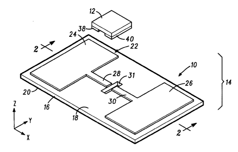
Referring to FIG. 1 of the drawings, shown in exploded assembly
view a radio frequency identification tag 14 includes a radio frequency
identification tag circuit chip ("circuit chip") 12 secured to an antenna 10.
Antenna 10 may form the basis for or a portion of a personal identification
AMENpEO SHEET
CA 02334832 2001-12-13
_g_
badge, a ticket, a waybill, a label, a package container (such as a box or
envelope), a portion thereof of the Like. As will also be appreciated,
antenna 10 may also form a basis for a rdio frequency ident~cation tag
circuit chip assembly ~.~., ~,ubstrate and ao~ductive pattern) as described
in the efarernentioned United States Patent 6,107,920 entitled "Radio
Frequency Identification Tag Having an Article Integrated Antenna"
witha~tt departing from the fair scope of the present invention. As seen,
antenna 10 inGudes a conductive pattern 22 disposed upon a substrate
1 e.
With continued reference to FIG. 1, substrate 18 may be paper,
plastic (including polyester and metallzed polyester material), synthetic
paper, reinforced paper, cardboard, synthetic paper coated cardboard and
the tike chosen for the particular application. Substrate 16 Includes a first
surface 18 and a second surface 20. Formed on first surface 18 is a
conductive pattern 22 including a first antenna element 24 and ~ second
antenna elemerTt 26. F-~aah of ftrst enbenna element 24 end second
antenna element 26 are formed from a conductive material that is bonded
or otherwise formed on substrate 16. Most preferably, each of first
antenna element 24 and second antenna element 26 are formed by
2D printing, using a suitable printable conductive medium. For example, a
catbon/graphite based conductive ink forms an effective conductive
putt~rn 22 when printed onto paper and/or cardboard. Synthetic and
coated papers may alternatively be used, but at added cast. Silver and
other precious metal inks maybe used particularly for printing on plastic
materials, but are less preferred du~ to higher malaria! costs. Conductive
pattern 22 is shown to have an "H" shape as would be suitable for use in
an electrostatic application. It will be appreciated that o#her patterns more
suitable tv, for example, inductive couplin5l may be printed without
departing from the fair scope of the present invention. First antenna
element 24 is formed with a first coupling region 28 and second antenna
element 2B is formed with a second coupling region 80. First codpling
legion 28 end second coupling tegfon 3D extend towafd and are
separated by an aperture 31 formed in substrate 16 at generally the
center of the H shape.
CA 02334832 2000-12-13
_,_
1PEAJUS i 3 NOU 2000
With reference to FIG. 1 and FIG. 2, circuit chip 12 is formed with a
conductive pad 38 and a conductive pad 40 arranged for coupling to conductive
pattern 22. As shown, conducaive pad 38 and conductive pad 40 are "bumped"
pads. That is, they project outwardly from a lower surface 32 of circuit chip
12.
This is in contrast to "surface" pads, which are formed substantially coplanar
with
lower surface 32 of a circuit chip. When secured to antenna 10, conductive pad
38 electrically couples to first coupling region 28 and conductive pad 40
electrically couples to second coupling region 30. As shown in FIG. 2, a layer
of
conductive adhesive 34 and a layer of conductive adhesive 36 are respectively
disposed between conductive pad 38 and first coupling region 28 and between
conductive pad 40 and second coupling region 30 providing the electrical
coupling and bonding circuit chip 12 to antenna 10. In a preferred embodiment
of the present invention an isotropic adhesive is used and accurately applied
to
either or both of circuit chip 12: and antenna 10. Alternatively, an
anisotropic
adhesive may be used but at a cost penalty. It should also be noted that no
particular preference exists for the use of bumped pads, and either bumped
pads, surface pads or recessed pads (i.e., canductive pads formed recessed
into
an outer surface of circuit chip 12) may be used, selected based upon cost and
the particular application. In the past, circuit chip 12 has been available
from
Temic North America, Inc., Basking Ridge, New Jersey as well as from Indala
Corporation, a wholly-owned subsidiary of Motorola, Inc., San Jose,
California.
A preferred anisotropic adhesive is 3M 9703 adhesive available from 3M
-- Corporation. The preferred adhesive is anisotropic in that it conducts in
the "z" or
vertical direction only (FIG. 2). The adhesive is manufactured to include
metallic
coated micro-sized pellets in an adhesive substrate that make electrical
contact
from a top surface to a lower surface of an adhesive layer. Electrical contact
is
not made in either of the "x" or "y" directions, i.e., the plane of the
adhesive layer.
Thus, adhesive may be applied in a complete la~ er without shorting across
adjacent conductors. A preferred isotropic adhesive is # 8103 available from
Adhesives Research, Inc.
AMENDED SHEET
CA 02334832 2000-12-13 C/T/US 9 9 ~ 13 6
~S 13 NOU 2000
_8_
To assist in the understanding of the present invention, and
referring to FIG. 3, antenna 10' is shown in an intermediate processing
stage. Antenna 10' represents an intermediate manufacturing stage of
antenna 10. For clarity, primed reference numerals are used to identify
elements that are not completely formed at this intermediate stage.
Referring then to FIG. 3, antenna 10' is formed by first forming, preferably
by printing, conductive pattern 22' on substrate 16'. As can be seen,
aperture 31 has not yet been formed, and first coupling region 28' joins
second coupling region 30' at the center of conductive pattern 22'.
FIG. 3 also illustrates the manufacturing tolerances associated with
forming conductive pattern 22' on substrate 16'. A discussion of these
-- tolerances and the effect they have on a completed antenna 10 will
provide additional insight as to the advantages of the present invention.
With reference to FIG. 3, even with very accurate printing processes,
conductive pattern 2~'.' will vary in both the "x" and "y" directions with
respect to an edge 42 and an edge 44, respectively, of substrate 16'.
Typically, the variation, respectively indicated as +/- x and +/- y, is on the
order of about +/- 0.5 mrn in each direction. In addition, and with
reference to FIG. 4, periphery 45 of conductive pattern 22' is not a sharp
line, but instead, "bleeding" of the conductive ink as a result of non-
uniform drying causes periphery 45 to have a rough profile. The variation
of periphery 45, indicated as +/- a in FIG. 4, can be as much as +I- 0.125
mm. Total variation resulting from both pattern position variation and
bleeding can range a:; high as +/- 1.5 mm. Significant in this number is
the fact that circuit chip 12 is 1 mm square. Thus, the variation of the
conductive pattern may be larger than circuit chip 12. As a result,
positioning circuit chip 12 to conductive pattern 22 referencing only edge
42 and edge 44 is impossible. Automated attachment of circuit chip 12
therefore requires sophisticated, expensive vision technology to
accurately locate the position of conductive pattern 22 on substrate 16.
The alternative to expensive vision automation is manual attachment.
Manual attachment is time consuming and does not offer the process
repeatability of automation. In either case, cost, quality and process
efficiency suffers tremendously.
AMENDED SHEET
CA 02334832 2000-12-13 PCTIUS 9 9 / 13 6 ~ 5
tP~Ws y 3 Nov zooo
_g_
With reference then to FIG. 5, antenna 10 in a completed stage
includes aperture 31 formed in substrate 16 separating first coupling
region 28 and second coupling region 30. In accordance with a preferred
embodiment of the present invention, aperture 31 is formed by punching
out a portion of substrate 16 at a center of conductive pattern 22 relative
to a substrate reference.
With continued reference to FIG. 5 and reference to FIG. 6,
antenna 10' is positioned to a fixture 100. Fixture 100 includes corner
locator block 102 and edge locator block 104 extending above a base
106. An alternate positioning arrangement may use pins engaging locator
holes/slots formed in substrate 16'. Corner locator block 102 is arranged
to engage both edge 42 and edge 44, with edge 42 and edge 44 providing
the substrate reference. Edge locator block 104 is arranged to engage
edge 44. In this manner, a consistent, repeatable reference for forming
an aperture 31 is established with respect to edge 42 and edge 44. Also
secured relative to fixture 100, and shown in FIG. 6, is a punch 108. In
operation, antenna 10' is positioned with respect to corner locator block
102 and edge locator block 104 on base 106. Punch 108 en~aqes
conductive pattern 22'' and substrate 16' shearing a plug 112 therefrom as
punch 108 passes through conductive pattern 22' and substrate 16' and
into button aperture 120. Aperture 31 thus precisely separates first
coupling region 28' and second coupling region 30'. Moreover, first
._ coupling region 28' and second coupling region 30' are precisely located
with respect to edge 42 and edge 44 making simplified automated
attachment of circuit chip 12 possible. It is anticipated that an edge 46 of
first coupling region 28' and an edge 48 of second coupling region 30'
may be formed to within ~/- 0.025 mm, respectively, from edge 42 and
edge 44.
In completing a. radio frequency identification tag 14 in accordance
with preferred embodiments of the present invention, circuit chip pick-and-
place automation (not shown) may be arranged to reference edge 42 and
edge 44. From this reference, a circuit chip 12 may be accurately
positioned with respect to first coupling region 28' and second coupling
region 30'. It should be further appreciated that a single
manufacturing/assembiy cell may be constructed. Such an assembly cell
FENDED SHEET
CA 02334832 2000-12-13 PCT/US 9 9 l 13 6 ,~
~PE~/US 13 NOU 2000
-10-
would provide for automated placement of substrate 16', printing using a
suitable print head conductive pattern 22', forming an aperture 31, and
positioning the circuit chip 12. However, in accordance with preferred
embodiments of the present invention, each of these operations may be
completed in separate manufacturing/assembly cells arranged, for
example, in production line fashion. Accurate formation of first coupling
region 28' and second coupling region 30' with respect to substrate 16',
and accurate placement of a circuit chip 12 with respect to these regions
is maintained throughout the process. Thus, the present invention
advantageously provides substantial manufacturing flexibility.
Referring to FIG. 7, an alternate preferred embodiment of the
present invention is shown. Again, antenna 10' represents an
intermediate manufacauring stage of antenna 10. For clarity, primed
reference numerals acre used to refer to elements that are not completely
formed at this interm~:diate stage (as shown in FIG. 3). As seen in FIG. 7,
punch 208 is arranged to sever conductive pattern 22' and surface 18'
and campress a portion of substrate 16' without forming a through
aperture in substrate 16'. Fixture 100 is constructed as before and
includes corner locator block 102 and edge locator block 104. Button
aperture 120 is omitted. Punch 208 engages conductive pattern 22' and
surface 18' at the interface of first coupling region 28' and second
coupling region 30' sE:vering conductive pattern 22' and surface 18' at the
point of engagement. Punch 208 further compresses a portion of
substrate 16' such that an indentation 231 is created separating first
coupling region 28' from second coupling region 30'. Again, very precise
location of first coupling region 28' and second coupling region 30' is
obtained with respect to edge 42 and edge 44 thereby permitting
automated placement of a circuit chip 12. In FIG. 8, punch 308 is
arranged with a bladed edge 330 to better pierce conductive pattern 22'
and surface 18' for forming an indentation 331 in substrate 16'.
With reference then to FIG. 9, in completing a radio frequency
identification tag 214 in accordance with preferred embodiments of the
present invention, circuit chip pick-and-place automation (not shown) may
be arranged to reference edge 42 and edge 44 of substrate 16' (edge 42
shown in FIG. 9). f=rom this reference; circuit chip 12 may be accurately
AMENDED SHEET
CA 02334832 2000-12-13 PCT/US 9 9 ~ 13 6
IPEA/US ~ 3 NOU 2000
-11-
positioned with conductive pad 38 electrically coupled via adhesive 34 to
first coupling region 28 and conductive pad 40 electrically coupled via
adhesive 36 to second coupling region 30. First coupling region 28 and
second coupling region 30 are precisely located and electrically isolated
via indentation 231 extending through conductive pattern 22 and surface
18 and into substrate 16.
FIG. 10 illustrates still another alternate preferred embodiment of
the present invention for forming an antenna 110. Fixture 200 includes
corner locator block 202 and an edge locator block (not shown) extending
above a base 406. An alternate locating arrangement may use locator
pins engaging holes/slots formed in substrate 116'. Corner locator block
202 is arranged to engage two edges of substrate 116' (edge 142 shown
in FIG. 10) and the edge locator block is arranged to engage one edge of
substrate 116' as described. Also secured relative to fixture 200 is a
forming/punch 408. Punch 408 includes a punch portion 410 arranged to
engage conductive pattern 122' and substrate 116' shearing a plug 412
therefrom as it passea through conductive pattern 122' and substrate 116'
and into button aperture 420. In this manner, an aperture 431 is formed in
substrate 116 separating coupling region 128 and coupling region 130.
Moreover, first coupling region 128 and second coupling region 130 are
precisely located with respect to the edges of substrate 116 making
simplified automated attachment of circuit chip 112 possible.
Punch 408 is further arranged with a shoulder or forming portion
424. As punch 408 engages substrate 116, a localized region 418 of
substrate 116 is compressed and formed to substantially correspond to
the shape of shoulder 424. In this manner, a recess 416 is formed in
substrate 116 adjacent aperture 431 and into which first coupling region
128 and second coupling region 130 extend.
With reference then to FIG. 11, a radio frequency identification tag
414 is assembled using antenna 110. In accordance ~nrith preferred
embodiments of the present invention, circuit chip pick-and-place
AMENDED SHEET
CA 02334832 2000-12-12
WO 99/67754 PCTIUS99/13b45
-12-
automation (not shown) may be arranged to reference the edges of
substrate 116 (edge 142 shown in FIG. 11 ). From this reference, circuit
chip 112 may be accurately positioned with conductive pad 138
electrically coupled via adhesive 134 to first coupling region 128 and
conductive pad 140 electrically coupled via adhesive 136 to second
coupling region 130. First coupling region 128 and second coupling
region 130 are precisely located and isolated from each other via aperture
431 extending through conductive pattern 122 and substrate 116. In this
manner, circuit chip 112 is coupled to each of first antenna element 124
and second antenna element 126 disposed on surface 118 of substrate
116. In addition, circuit chip 112 is maintained below surface 118 thereby
reducing the potential for it becoming dislodged from substrate 116 during
use of radio frequency identification tag 414. It should also be
appreciated that a potting material and/or a cover may be disposed over
circuit chip 112 thereby offering further protection.
In summary, and referring again to FIG. 1, a radio frequency
identification tag 14 includes a radio frequency identification tag circuit
chip 12 secured to an antenna 10. The antenna includes a first antenna
element 24 and a second antenna element 26 formed on a surface 18 of
a substrate 16. The first antenna element and the second antenna
element are separated and precisely located by an aperture 31 formed in
the substrate.
Referring to FIG. 7 and FIG. 8, alternative preferred embodiments
of antenna 10 include a first antenna element 24 and a second antenna
element 26 formed on a surface 18 of a substrate 16. The first antenna
element and the second antenna element are separated and precisely
located by an indentation 231 and 331, respectively shown in FIG. 7 and
FIG. 8, formed through the surface and extending partially into the
substrate.
With reference to FIG. 9, a radio frequency identification tag 214
includes a radio frequency identification tag circuit chip 12 secured to an
antenna 10. The antenna includes a first antenna element 24 and a
second antenna element 26 formed on a surface 18 of a substrate 16 with
the first antenna element and the second antenna element being
CA 02334832 2000-12-12
WO 99/67754 PCT/US99/13645
-13-
separated and precisely located by an indentation 31 formed in the
substrate.
In yet another preferred embodiment of the present invention, and
with reference to FIG. 10, an antenna 110 includes a first antenna
element 124 and a second antenna element 126 formed on a surface 118
of a substrate 116. The substrate is formed to include a recess 416
formed in the substrate. The first antenna element includes a first
coupling region 128 and the second antenna element includes a second
coupling region 130. The first coupling region and the second coupling
region extend into the recess and are separated and precisely located by
an aperture 431 formed in the recess.
With reference to FIG. 11, a radio frequency identification tag 414
includes a radio frequency identification tag circuit chip 112 secured to an
antenna 110. The antenna includes a first antenna element 124 and a
second antenna element 126 formed on a surface 118 of a substrate 116.
Antenna 110 also includes a recess 416 formed in substrate 116 and a
first coupling region 128 and a second coupling region 130 extending into
the recess and separately and precisely located by an aperture 431
formed in the recess. A radio frequency identification tag circuit chip is
secured in the recess and is coupled to the first coupling region and the
second coupling region. The first coupling region and the second
coupling region thereby couple the radio frequency identification tag circuit
chip to the first antenna element and the second antenna element.
In accordance with a preferred method of making a radio frequency
identification tag, a substrate having a surface is provided. A conductive
pattern is printed on the surface, and an aperture is formed in the
substrate relative to a substrate reference, the aperture separating the
conductive pattern into a first antenna element and a second antenna
element. A radio frequency identification tag circuit chip is then secured
to the substrate and electrically coupled to the first antenna element and
the second antenna element. The method may alternatively provide for
forming an indentation andlor a recess in the substrate.
Some advantages of the present invention are now discussed.
Limitations in the ability to control dimensian and position
tolerances of printed antennas have limited this cost effective and
CA 02334832 2000-12-12
WO 99/67754 PCT/US99/13645
-14-
performance enhancing technology in radio frequency identification tags.
The present invention facilitates the use of printed antenna technology by
overcoming these tolerance limitations.
Radio frequency identification tag cost is reduced while
performance is increased through the use of printed antennas that may be
easily mated to radio frequency identification tag circuit chips.
Manufacturing efficiency is improved by the present invention in
that radio frequency identification tag circuit chips are quickly and
accurately secured and coupled to a radio frequency identification tag
antenna.
The present invention also allows for the economical manufacture
of radio frequency identification tags in single cell or multiple cell
manufacturing arrangements using commonly available pick-and-place
automation.
Many additional changes and modifications could be made to the
invention without departing from the fair scope and spirit thereof. The
scope of some changes is discussed above. The scope of others will
become apparent from the appended claims.
I claim: