Note: Descriptions are shown in the official language in which they were submitted.
CA 02346733 2005-10-14
-1-
OMNIDIRECTIONAL REFLECTIVE MULTILAYER DEVICE FOR CONFINING
ELECTROMAGNETIC RADIATION
BACKGROUND OF THE INVENTION
The invention relates to the field of optical waveguiding, and in particular
to
an omnidirectional multilayered device for enhanced waveguiding of
electromagnetic
radiation.
Mirrors are probably the most prevalent of optical devices. Known to the
ancients and used by them as objects of worship and beauty, mirrors are
currently employed
for imaging, solar energy collection and in laser cavities. Their intriguing
optical properties
have captured the imagination of scientists as well as artists and writers.
One can distinguish between two types of mirrors, the age-old metallic, and
more recent dielectric. Metallic mirrors reflect light over a broad range of
frequencies
incident from arbitrary angles, i.e., omnidirectional reflectance. However, at
infrared and
optical frequencies, a few percent of the incident power is typically lost due
to absorption.
Multilayer dielectric mirrors are used primarily to reflect a narrow range of
frequencies
incident from a particular angle or particular angular range. Unlike their
metallic
counterparts, dielectric reflectors can be extremely low loss.
The ability to reflect light of arbitrary angle of incidence for all-
dielectric
structures has been associated with the existence of a complete photonic
bandgap, which
can exist only in a system with a dielectric function that is periodic along
three orthogonal
directions. In fact, a recent theoretical analysis predicted that a sufficient
condition for the
achievement of omnidirectional reflection in a periodic system with an
interface is the
existence of an overlapping bandgap regime in phase space above the light cone
of the
ambient media.
The theoretical analysis is now extended to provide experimental realization
of a multilayer omnidirectional reflector operable in infrared frequencies.
The structure is
made of thin layers of materials with difference dielectric constants
(polystyrene and
tellurium) and combines characteristic features of both the metallic and
dielectric mirrors.
It offers metallic-like omnidirectional reflectivity together with frequency
selectivity and
low-loss behaviour typical of multilayer dielectrics.
CA 02346733 2006-04-24
-2-
SUMMARY OF THE INVENTION
According to one aspect of the invention, there is provided a device
comprising: a dielectric inner core surrounded by an outer dielectric region
comprising a
plurality of alternating layers of high-index and low-index dielectric
materials, the outer
dielectric region confining electromagnetic radiation to the inner core
region, wherein the
refractive indices of the dielectric materials, the number of the alternating
layers in the outer
dielectric regions, and the thicknesses of the alternating layers result in a
reflectivity that is
greater than 95% for all angles of incidence from the inner core region to the
outer dielectric
region ranging from 0° to at least 80° for all polarizations for
at least one range of
frequencies of the electromagnetic radiation, the at least one range of
frequencies dependent
on the refractive indices of the dielectric materials and the thicknesses of
the alternating
layers, and wherein sin-' ( n~ I n y )< tan-' ( n, l n, ), no < n, , and n~ <
n, where no is the
I S refractive index of the dielectric inner core, n, is the refractive index
of the high-index
dielectric material layer, and n, is the refractive index of the low-index
dielectric material
layer.
According to another aspect of the invention, there is provided a waveguide
which exhibits omnidirectional reflection, comprising: a dielectric inner core
region
surrounded by an outer dielectric region comprising a plurality of alternating
layers of high-
index and low-index dielectric materials, the outer dielectric region
confining
electromagnetic radiation to the inner core region, wherein the refractive
indices of the
dielectric materials, the number of the alternating layers in the outer
dielectric regions, and
the thicknesses of the alternating layers result in a reflectivity that is
greater than 95% for all
angles of incidence from the inner core region to the outer dielectric region
ranging from 0°
to at least 80° for all polarizations for at least one range of
frequencies of the
electromagnetic radiation, the at least one range of frequencies dependent on
the refractive
indices of the dielectric materials and the thicknesses of the alternating
layers, and wherein
sin' ( n~ /n, )< tan-' ( n, l n2 ), n~ < n, , and no < n, , where no is the
refractive index of the
dielectric inner core, n, is the refractive index of the high-index dielectric
material layer,
and n, is the refractive index of the low-index dielectric material layer.
CA 02346733 2006-04-24
-2a-
According to another aspect of the invention, there is provided a device
comprising: a dielectric inner core region surrounded by an outer dielectric
region
comprising a plurality of alternating layers of high-index and low-index
dielectric materials,
the outer dielectric region confining electromagnetic radiation to the inner
core region,
wherein the layers in the outer dielectric layer define a refractive index
variation that
produce a range of frequencies for which there is omnidirectional reflection
for
electromagnetic radiation incident on the dielectric outer region from the
dielectric inner
core region, the range of frequencies for which there is omnidirectional
reflection being
defined from above by an upper frequency denoted as ~h corresponding to a
photonic band
edge for normally incident electromagnetic radiation and from below by a lower
frequency
denoted as ~, corresponding to an intersection between a photonic band edge
for TM
electromagnetic radiation and a light line defined by the dielectric inner
core region,
wherein coi, and con are dependent on the refractive indices of the dielectric
material and the
thicknesses of the alternating layers, and wherein sin-' ( no /n, )< tan-' (
n, l n, ), n~ < n, , and
no < n, , where n~ is the refractive index of the dielectric inner core, n, is
the refractive
index of the high-index dielectric material layer, and n, is the refractive
index of the low-
index dielectric material layer.
According to another aspect of the invention, there is provided a device
comprising: a dielectric inner core region surrounded by an outer dielectric
region
comprising a plurality of alternating layers of high-index and low-index
dielectric materials,
the outer dielectric region confining electromagnetic radiation to the inner
core region,
wherein the refractive index of the dielectric inner core regions is n~ , the
refractive indices
of the high-index and low-index materials are n, and n, , respectively, the
thicknesses of
the high-index and low-index layers are h, and h, , respectively, and n, > n,
> no , wherein
the indices satisfy sin-' ( no /n2 )< tan-' ( n, l n, ), and wherein the
indices and thicknesses are
selected so as to satisfy, ~,, > ~, , where w,, and ~, are two predetermined
frequencies
given by the respective expressions:
CA 02346733 2006-04-24
-2b-
2c _, n, - n2
cos ,
h2nz + h, n, n, + n2
2c cos-' n' nz n° n2 n? no
h2 n2 - no + h~ n; - no n; n2 - no + n2 n; - no
whereby the outer dielectric region reflects the electromagnetic radiation for
all angles of
incidence within a predetermined angle range when the frequency of the
electromagnetic
radiation cv is in the range from coi to coh.
According to another aspect of the invention, there is provided a device for
confining electromagnetic radiation, comprising: a dielectric inner core
region in which the
electromagnetic radiation is to be confined, the inner core region having a
refractive index
no , an outer dielectric region surrounding the inner core region to confine
the
electromagnetic radiation within the inner core region, the outer dielectric
region including
a plurality of alternating layers of high-index and low-index dielectric
materials surrounding
the core region, wherein the refractive indices of the high-index and low-
index materials are
n, and n, , respectively, the thicknesses of the high-index and low-index
layers are h, and
h, , respectively, and n, > n, > no , wherein the refractive indices and
thicknesses are selected
so as to satisfy, ~,, > ~, , where ~,, and r.~, are two predetermined
frequencies given by the
respective expressions:
2c _, n, - nz
cos , and
hZn2 + h,n, n, + n2
2c cos-' n' n2 n° n2 n' no
h2 n2 - no + h, n; - no n; n2 - no + n2 n; - no
to provide a range of frequencies between the predetermined frequencies co, to
co,, for which
the alternating layers provide omnidirectional reflectivity for
electromagnetic radiation
incident on the alternating layers from the inner core region, and wherein the
number of
CA 02346733 2006-04-24
-2 c-
alternating layers are sufficient to cause omnidirectional reflectivity to be
greater than 95%
electromagnetic radiation incident on the alternating layers from the inner
core region at all
angles ranging from 0° to 80° and all polarizations for all
frequencies in the omindirectional
range of frequencies between co, to co,,.
BRIEF DESCRIPTION OF THE DRAWINGS
FIG. 1 is a simplified block diagram of an exemplary embodiment of a
multilayer periodic dielectric film structure in accordance with the
invention;
FIG. 2A is a graph of the projected band structure of a multilayer film with a
light line and Brewster line, exhibiting a reflectivity range of limited
angular acceptance;
FIG. 2B is a graph of the projected band structure of a multilayer film
together with the
light line and Brewster line, showing an omnidirectional reflectance range at
the first and
second harmonic;
FIG. 3 is a graph of the range to midrange ratio for the fundamental
frequency range of omnidirectional reflection plotted as contours;
FIG. 4 is a series of graphs showing the calculated (solid line) and measured
(dashed line) reflectance (%) as a function of wavelength for TM and TE modes
at normal,
45°, and 80° angles of incidence, thus showing an
omnidirectional reflectivity band;
FIG. 5 is a table showing that ~ is a monotonically increasing function of the
incident angle for the TM mode of an omnidirectional reflector;
FIG. 6A is a simplified block diagram cross section of an exemplary
structure
CA 02346733 2001-04-09
WO 00/22466 PCTNS99/23833
-3-
FIG. 6B is a corresponding cross section radial index of refraction profile of
the struchu~e
in FIG. 6A; and
FIG. 7 is a cross section of a simplified schematic diagram of a coextrusion
assembly in accordance with the invention.
DETAILED DESCRIPTION OF THE INVENTION
FIG. 1 is a simplified block diagram of an exemplary embodiment of a
muitilayer
periodic dielectric film structure 100 in accordance with the invention. The
structure is
made of an array of alternating dielectric layers 102,104 coupled to a
homogeneous
medium, characterized by no (such as air with no = 1 ), at the interfaces.
Electromagnetic
waves are incident upon the multilayer film from the homogeneous medium. The
possibility of omnidirectional reflectivity for such a system has now been
recognized. h,
and h2 are the layer thickness , and n, and n_ are the indices of refraction
of the
respective layers 104 and 102.
An exemplary incident wave has a wave vector k = kxex + kyey and frequency of
w = c~k~ . The wave vector together with the normal to the periodic structure
100 defines
a minor plane of symmetry that allows distinguishing between two independent
electromagnetic modes: transverse electric (TE) modes and transverse magnetic
(TM)
2 0 modes. For the TE mode, the electric field is perpendicular to the plane,
as is the
magnetic field for the TM mode. The distribution of the electric field of the
TE mode (or
the magnetic field in the TM mode) in a particular layer within the stratified
structure can
be written as a sum of two plane waves traveling in opposite directions. The
amplitudes
of the two plane waves in a particular layer a of one cell are related to the
amplitudes in
the same layer of an adjacent cell by a unitary 2x2 translation matrix U~"~
General features of the transport properties of the finite structure can be
understood when the properties of the infinite structure are elucidated. In a
structure with
infinite number of layers, translational symmetry along the direction
perpendicular to the
layers leads to Bloch wave solutions of the form
iKx ikry
E,~ ~x, y) = E,~ (x~ a ,
where Ex (x) is periodic, with a period of length a, and K is the Bloch wave
number
given by
CA 02346733 2005-10-14
-4-
K= aln ~Tr(U~°~)~ 4(Tr(U~°~)Z -1)l
(2)
where Tr denotes the trace operation, which yields the sum of the diagonal
matrix elements.
Solutions of the infinite system can be propagating or evanescent,
corresponding to real or
imaginary Bloch wave numbers, respectively. The solution of Eq. 2 defines the
band
structure for the infinite system, cu (K,ky).
It is convenient to display the solutions of the infinite structure by
projecting
the w (K,ky) function onto the w - ky plane. FIGs. 2A and 2B are examples of
such
projected structures.
FIG. 2A is a graph of the projected band structure of a multilayer film with a
light line 200 and Brewster line 202, exhibiting a reflectivity range of
limited angular
acceptance with n1 = 2.2 and n2 = 1.7, and a thickness ratio of h2 / hl = 2.2
/ 1.7.
FIG. 2B is a graph of the projected band structure of a multilayer film
together with the light line 204 and Brewster line 206, showing an
omnidirectional
reflectance range at the first and second harmonic. The film parameters are n1
= 4.6 and n2
= 1.6 with a thickness ratio of h2 / hl = 1.6 / 0.8. These parameters are
similar to the actual
polymer-tellurium film parameters measured in the experiment.
The area 208 and 210 (light gray) highlight phase space where K is strictly
real, i.e., regions of propagating states. The area 212 (white) represents
regions containing
evanescent states. The areas 214 and 216 represent omnidirectional reflectance
ranges.
The shape of the projected band structures for the multilayer film structure
can be understood intuitively. At ky = 0 the bandgap for waves travelling
normal to the
layers is recovered. For ky > 0, the bands curve upward in frequency. As ky ~
oo , the
modes become largely confined to the slabs with the high index of refraction
and do not
~5 rrnmla llPtWlP! n lavPre ~an~l arP thPrPfnrP mrlananrlPnt of lrxl
CA 02346733 2004-07-15
-4a-
For a finite structure, the translational symmetry in the directions parallel
to the layers is
preserved, hence ky remains a conserved quantity. In the direction
perpendicular to the
layers, the translational symmetry no longer exists. Nevertheless, the K
number, as defined
in Eq. 2, is still relevant, because it is determined purely by the dielectric
and structural
property of a single bilayer. In regions where K is imaginary, the
electromagnetic field is
strongly attenuated. As the number of layers is increased, the transmission
coefficient
_________ __________~:_»__ ___tm_ n__ __n__~:__:~__ _~___.._t_.. __~:4_.
CA 02346733 2001-04-09
WO 00/22466 PCT/US99/Z3833
-5-
Since the primary interest is in waves originating from the homogeneous medium
external to the periodic structure, the focus will be only on the portion of
phase space
lying above the light line. Waves originating from the homogeneous medium
satisfy the
condition w >_ cky l no, where no is the refractive index of the homogeneous
medium, and
therefore they must reside above the light line. States of the homogeneous
medium with
ky = 0 are normal incident, and those lying on the w = cky l no line with kx =
0 are
incident at an angle of 90°.
The states in FIG. 2A that are lying in the restricted phase space defined by
the
light line 200 and that have a (w , k y ) corresponding to the propagating
solutions (gray
areas 208) of the structure can propagate in both the homogeneous medium and
in the
structure. These waves will partially or entirely transmit through the film.
Those with
(w, ky) in the evanescent regions (white areas 212) can propagate in the
homogeneous
medium, but will decay in the structure. Waves corresponding to this portion
of phase
space will be reflected off the structure.
The multilayer system leading to FIGS. 2A represents a structure with a
limited
reflectivity cone since for any frequency one can always find a ky vector for
which a
wave at that frequency can propagate in the structure, and hence transmit
through the film.
For example, a wave with w = 0.285 2~cla (dashed horizontal line 218) will be
reflected
for a range of ky values ranging from 0 (normal incidence) to 0.285 2n/a
(90° incidence)
2 0 in the TE mode, while in the TM mode it begins to transmit at a value of
ky = 0.187 2~/a
('41° incidence). The necessary and sufficient criterion for
omnidirectional reflectivity
at a given frequency is that there exist no transmitting states of the
structure inside the
Light cone. This criterion is satisfied by frequency ranges 214 and 216 in
FIG. 2B. In
fact, the system leading to FIG. 2B exhibits two omnidirectional reflectivity
ranges.
A necessary condition for omnidirectional reflectivity is that light from
outside of
the structure cannot be allowed to access the Brewster angle 6 B = tan-' (n, l
n2 ) of the
multilayer structure because at this angle, the TM mode will be transmitted
through. This
condition is met when the Brewster line lies outside of the light line, or,
terms of the
refractive indices of the layers, siu-' (»o / n?) < AB . A sufficient
condition is the existence
3 0 of a particular frequency at which no propagating mode within the crystal
exists between
ky =Oand ky =wlc.
CA 02346733 2004-07-15
-6-
FIG. 2A is an example of a structure, which does not have an
omnidirectional reflectivity range even though its Brewster crossing is
inaccessible to light
coming from the homogeneous medium (the Brewster crossing lies outside of the
light
cone). This is due to the large group velocity of modes in the lower band edge
of the TM
mode which allow every frequency to couple to a propagating state in the
crystal. This
should be contrasted with FIG 2B, which exhibits an omnidirectional
reflectivity (area 214).
The high indices of refraction actually allow for the opening of an additional
omnidirectional reflectivity range (area 216) in the higher harmonic as well.
The omnidirectional range is defined from above by the normal incidence
band edge ~h ~kx = ~ l a, ky = 0~ (point 220), and below by the intersection
of the top of the
TM allowed band edge with the light line ~~ ~kx = ~ l a, ky = noc~, l c~
(point 222). The
exact expression for the band edges is
1 2n cos~kX'~h, + k~z~hz )+ 1 2n cos~kx'~h, - kXZ~hz ~+ 1= 0, (3)
s
where kx"~ = pvna l c)2 - ky ~a = l, 2) and
_1 k~2~ k~'~
2 k~'~ + k~z~ TE
x x
_1 nzk~2~ nZk~'~ ~4)
x z x TM.
2 nZk~'~ + n2k~2~
2 x 1 x
CA 02346733 2004-07-15
-6a-
A dimensionless parameter used to quantify the extent of the omnidirectional
reflection
range is the range to midrange ratio defined as ~~h - to, ~l ~ ~r~h + to, ~.
FIG. 3 is a plot of
this ratio as a function of n2 / n, and n, l n° where r,~h and w, are
determined by solutions of
Eq. 3 with quarter wave layer thickness, and n2 )n, . The contours in this
figure represent
various equi-omnidirectional ranges for different material index parameters
and could be
useful for design purposes. The ratio for the exemplary materials is
approximately
45% ~n, l n2 = 2.8?5, n2 ! n° =1.6~, and it is located at the
intersection of the dashed lines at
point 300.
It may also be usefi~l to have an approximate analytical expression for the
extent of the gap, where the "gap" is the frequency range between the edges of
the allowed
bands. This can be obtained by setting cos~kx'~h, - kxz~h2 ~ ~ 1 in Eq. 3. It
is found that for a
~...us.~ .w..:~7.....4 ......'1.. ~ 41.... ..._."...,_._~....~._ __.:.14L ~~
L~.._~___~-__ _-
CA 02346733 2004-07-15
_'7_
0~~90 ) = 2c cos-' n + 1 - cos-' n + 1 ~ ~5)
z z ~ z z-nzsi z8
h~ n~ - no stn Io + hz nz ° n o
At normal incidence there is no distinction between TM and TE modes. At
increasingly
oblique angles the gap of the TE mode increases, whereas the gap of the TM
mode
decreases. In addition, the center of the gap shifts to higher frequencies.
Therefore, the
criterion for the existence of omnidirectional reflectivity can be restated as
the occurrence of
a frequency overlap between the gap at normal incidence and the gap of the TM
mode at
90° . Analytic expressions for the range to midrange ratio can be
obtained by setting
2c _, n, - nz
toh = cos ,
hznz + h,n, n1 + nz
(6)
- 2c cos-' n' nz n° nz n' no
hz n2 no + h, n; no n; n2 no + ni n~ no
Moreover, the maximum range width is attained for thickness values that are
not equal to the quarter wave stack though the increase in bandwidth gained by
deviating
from the quarter wave stack is typically only a few percent.
In general, the TM mode defines the lower frequency edge of the
omnidirectional range. An example can be seen in FIG. 2B for a particular
choice of the
indices of refraction. This can be proven by showing that
a~ ~ a~
ax ax
Y TM y TE
CA 02346733 2004-07-15
-7a-
in the region that resides inside the light line. The physical reason for Eq.
7 lies in the
vectorial nature of the electric field. In the upper portion of the first band
the electric field
concentrates its energy in the high dielectric regions.
Away from normal incidence the electric field in the TM mode has a
component in the direction of periodicity. This component forces a larger
portion of the
electric field into the low dielectric regions. The group velocity of the TM
mode is
therefore enhanced. In contrast, the electric field of the TE mode is always
perpendicular to
the direction of periodicity and can concentrate its energy primarily in the
high dielectric
1 d region.
A polystyrene-tellurium (PS-Te) materials system was chosen to demonstrate
omnidirectional reflectivity. Tellurium has a high index of refraction and low
loss
CA 02346733 2005-10-14
_g_
characteristics in the frequency range of interest. In addition, its
relatively low latent heat
of condensation together with the high glass transition temperature of the PS
minimizes
diffusion of Te into the polymer layer. The choice of PS, which has a series
of absorption
peaks in the measurement range, demonstrates the competition between
reflectivity and
absorption that occurs when an absorption peak is located in the evanescent
state region.
The Te(0.8pm) and PS (1.65pm) films were deposited sequentially to create a
nine-layer
film.
A 0.8 ~ 0.09pm thick layer of tellurium (99.99 + %, Strem Chemicals) was
vacuum evaporated at 10-6 torr and 7A (Ladd Industries 30000) onto a NaCI 25mm
salt
substrate (polished NaCI window, Wilmad Glass). The layer thickness and
deposition rate
were monitored in-situ using a crystal thickness monitor (Sycon STM100). A 10%
solution of polystyrene (Goodyear PS standard, 110,OOOg/mol) in toluene was
spin cast at
1000RPM onto the tellurium coated substrate and allowed to dry for a few
hours, the
polymer layer thickness is 1.65 ~ 0.09qm. The nine layer film sequence was
Te/PS/Te/PS/Te/PS/Te/PS/Te.
The optical response of this particular multilayer film was designed to have
a high reflectivity region in the 10 to 15~m range for any angle of incidence
(in the
experiment we measure from 0° to 80°). The optical response at
oblique angles of
incidence was measured using a Fourier Transform Infrared Spectrometer
(Nicolet 860)
fitted with a polarizer (ZnS SpectraTech) and an angular reflectivity stage
(VeeMax by
SpectraTech). At normal incidence, the reflectivity was measured using a
Nicolet Infrared
Microscope. A freshly evaporated aluminum mirror was used as a background for
the
reflectance measurements.
FIG. 4 is a series of graphs showing the calculated (solid line) and
measured (dashed line) reflectance (%) as a function of wavelength for TM and
TE modes
at normal, 45°, and 80° angles of incidence, thus showing an
omnidirectional reflectivity
band. FIG. 4 illustrates the good agreement between the calculated and
measured
reflectance spectra. The calculations were done using the transfer matrix
method
described in F. Abeles, Ann. De Physique 5, 706 (1950).
The regimes of high reflectivity at the different angles of incidence overlap,
thus forming a reflective range of frequencies for light of any angle of
incidence. The
frequency location of the omnidirectional range is determined by the layer
thickness and
CA 02346733 2004-07-15
-9-
can be tuned to meet specifications. The range is calculated from Eq. 6 to be
5.6 ~,m and
the center wavelength is 12.4 ~m corresponding to a 45% range to midrange
ratio shown in
dashed lines in FIG. 3 for the experimental index of refraction parameters.
These values are
in agreement with the measured data. The calculations are for lossless media
and therefore
do not predict the PS absorption band at ~ 13 and 14 microns. The PS
absorption peak is
seen to increase at larger angles of incidence for the TM mode, and decrease
for the TE
mode.
The physical basis for this phenomena lies in the relation between the
penetration depth and the amount of absorption. The penetration length is ~ oc
Im (1 / K),
with K the Bloch wave number. It can be shown that ~ is a monotonically
increasing
function of the incident angle for the TM mode of an omnidirectional
reflector, and is
relatively constant for the TE mode. Thus, the TM mode penetrates deeper into
the
structure at increasing angles of incidence and is more readily absorbed, as
is shown in the
table of FIG. 5. The magnitude of the imaginary part of the Bloch wave number
for a mode
lying in the gap is related to its distance from the band edges. This distance
increases in the
TE mode due to the widening of the gap at increasing angles of incidence and
decreases in
the TM mode due to the shrinking of the gap.
The PS-Te structure does not have a complete photonic bandgap. Its
2 0 omnidirectional reflectivity is due instead to the restricted phase space
available to the
propagating states of the system. The materials and processes were chosen for
their low
cost and applicability to large area coverage. In addition to
omnidirectionality, the
measurements show that a polymer, while lossy in the infrared, can still be
used for
CA 02346733 2004-07-15
-9a-
reflection applications without a considerable sacrifice of performance. The
possibility of
achieving omnidirectional reflectivity itself is not associated with any
particular choice of
material and can be applied to many wavelengths of interest. The structure of
the invention
offers metallic-like omnidirectional reflectivity for a wide range of
frequencies, and at the
same time is of low loss. In addition, it allows the flexibility of frequency
selection.
In accordance with the invention, the confinement of light in cavities and
wave guides using an omnidirectional multilayer film will now be described.
The
multilayer film structure has been described in commonly owned U.S. Patent
No. 6,130,780, issued October 10, 2000. Specifically, a method is presented
for creating
CA 02346733 2001-04-09
WO 00/22466 PCT/US99/23833
- 10-
low loss broad band optical fibers, which are capable of transmitting around
sharp bids.
In addition, a design is presented for improving the delivering power of a
near field
optical fiber tip.
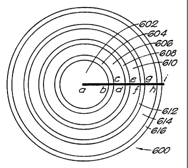
FIG. 6A is a simplified block diagram cross section of an exemplary structure
600.
FIG. 6B is a corresponding cross section radial index of refiaction profile of
the structure
600. The structure consists of concentric cylindrical layers 604-616 with
alternating
indices of refraction n,, n2 centered on a core 602 of low dielectric material
no , such as
air. The radius of the core is ha and the layer thicknesses are h" hz . Note
that an
exemplary embodiment would involve each layer consisting of different material
and
corresponding different layer thickness. 1fie parameters of the multilayer
film are chosen
such that light from any incident angle and polarization is completely
reflected by the
multilayer for the range of signal frequencies.
For example, for values of no, n,, n~, h,, and hZ as in FIG. 2B, light can be
guided
for any frequency within the two broadband omnidirectional reflection ranges
214 and
216. As is generally the case, the electromagnetic radiation will be mufti-
mode or singie
mode depending an the size of the region in which it is confined. Thus, within
each
broadband range the electromagnetic radiation can be mufti-mode or single mode
depending on the size of the inner core region. For large core radii, the
light will be
mufti-mode and for very small radii the light will be single mode.
Conventional optical fibers confine a propagating EM pulse by total internal
reflection where the electromagnetic (EM) wave travels through a high index
fiber core
surrounded by low-index cladding. In accordance with the invention, the method
of
confinement in the OmniguideT"' waveguide structure is the polarization
independent
omnidirectional reflectance of EM waves at the walls of the hollow fiber. The
advantages
of this mode of confinement are numerous.
There is very low loss associated with material absorption since the wave
travels
essentially through air, which is extremely low loss when compared with any
dense
medium. This enables low loss propagation which is of importance in basically
every
device that involves light guiding for communication, lasers and more.
3 0 Conventional optical communication fibers need amplification to compensate
for
absorption losses in the material, and to this end, the fiber is periodically
doped with
erbium. The use of erbium severely limits the bandwidth of the fiber. Since
the structure
of the invention is very low loss and does not need amplification, orders of
magnitude
CA 02346733 2001-04-09
WO 00/22466 PCTNS99/23833
-11-
increase in the usable bandwidth is possible. In addition, the omnidirectional
multilayer
structure provides a strong confinement mechanism and will propagate signals
around very
sharp bends as demonstrated in other systems with strong confinement
mechanisms.
Such a multilayer coated fiber will also be important for improving the
delivering
power of a fiber tip in a near-field scanning optical microscope. The tip is
used to deliver
optical power with a spot size far smaller than the wavelength of light. Metal
coattng is
currently employed in order to confine light to such a small length scale.
Metal coatings
have material absorption losses, which in this case limits the maximum
delivery power.
The fiber tip with a multilayer coating overcomes this problem since it is
essentially
1 0 lossless.
The ultimate goal is to create a hollow structure with walls made of a
multilayer
coating in accordance with the structure described heretofore. The structure
may be of,
but is not limited to, a cylindrical geometry. One method to produce such a
structure is
to take a thin wall hollow fiber made of glass or polymer and coat it with
alternating
layers of dielectrics. The layers could be made of a polymer or glass as the
low refiactive
index component, and Germanium or Tellurium as the high index material. One
would
then take the fiber and evaporate a layer of prescribed thickness using a
thermal
evaporator or sputtering device. The subsequent low index layer would be
deposited by
dipping the fiber in a dilute solution of the polymer, or by evaporating a
monomer
2 0 followed by a rapid polymerization.
Another exemplary method would be the coextrusion of the entire structure
using
a combination of immiscible polymers, one loaded with a high index component
in a fine
powder form the other without additives as in FIG. 7. FIG. 7 is a cross
section of a
simplified schematic diagram of a coextrusion assembly 700 in accordance with
the
invention. An extruding device 702 provides a structure 704 of alternating
layers of high
and low index polymer surrounding an air core 706.
Although the present invention has been shown and described with respect to
several preferred embodiments thereof, various changes, omissions and
additions to the
form and detail thereof, may be made therein, without departing from the
spirit and scope
of the invention.
What is claimed is: