Note: Descriptions are shown in the official language in which they were submitted.
CA 02348072 2003-03-05
-1-
TRANSCUTANEOUS ENERGY TRANSMISSION SYSTEM
WITH FULL WAVE CLASS E RECTIFIER
10 TECHNICAL FIELD
This invention relates generally to transcutaneous energy transmissions
systems.
In particular, the invention relates to the use of two coils to inductively
transmit radio
frequency power across an intact skin boundary for use by a device implanted
under the
skin, or otherwise within the body of, a living being.
BACKGROUND
Transcutaneous energy transfer systems (TETS) have been used to provide
power for a number of implanted devices such as: low power prosthetic devices;
cochlear implants, muscle stimulators, bone growth stimulators and stimulators
of the
visual cortex, and higher power devices; total artificial hearts, and
ventricular assist
devices. The inductively coupled coils of a TETS, one implanted under the
skin, the
other resting on the surface of the skin, permit electrical interaction
between the
implanted device and external circuits through intact skin, and bring about
the transfer
of power from the external circuit to the internal circuit avoiding
penetration of the skin
by electrical conductors. FIG. 1 illustrates a vertical cross section through
an
exemplary prior art TETS as implanted and in position for use.
The interaction between the coils requires alternating current; usually a
frequency between 100 kHz and 1 MHz is chosen. In order to improve the
efficiency
with which power is delivered, the coils are incorporated into either series
or parallel
resonant circuits by connecting them to capacitors. The resonant circuits can
be tuned
with a natural resonant frequency less than, equal to, or greater than the
operating
frequency, as described by the U.S. Patent Nos. 4,441,210 and 5,070,535 to
Hochmair
et al. and U.S. Patent No. 4,679,560 to Galbraith. In the following
discussion, the
CA 02348072 2001-04-20
WO 00/24456 PCT/US99/25177
-2-
efficiency with which power is transferred to the internal coil will be
referred to as link
efficiency. This quantity is related to the overall efficiency of the TETS by
the
expression:
~overol! ~ (~DCtoRF'){~llnk)(~RFtoDC) ~1~
where, rl~ to RF 1S the efficiency of the transmitter circuit, rIRF ~o Dc is
the efficiency of the
receiver circuit and rl,;~~ is the efficiency of the inductive link between
the transmitter
circuit and the receiver circuit. Thus, the overall efficiency is equal to the
product of
three sequential process efficiencies.
DC to RF Conversion
LaForge in U.S. Patent No. 4,665,896 and Miller in U.S. Patent No. 5,350,413
describe the need to have an active control circuit to adjust the frequency of
the
circuitry driving the external resonant circuit such that a constant phase
relationship is
maintained between the drive voltage and the resonant current. With this "auto-
tuning"
circuit, as described by LaForge and Miller, the frequency of operation is
maintained at,
or near, the resonant frequency. Because of variable coupling between the
transmitter
and receiver coils, the resonant frequency is a function of relative coil
position.
Link Efficiency
In U.S. Patent No. 4,441,210 to Hochmair et al., resonant frequencies of both
the external and the internal circuits were implicitly tuned to the operating
frequency.
Hochmair et al. explicitly clarified this point in his U.S. Patent No.
5,070,535.
Hochmair et al. adjusted the quality factor, Q, of his circuits in order to
achieve critical
coupling and an output that was not sensitive to the relative position of the
coils. The
degree of coupling is indicated by the coupling coefficient, k, which is equal
to unity for
an ideal transformer and equal to zero for isolated coils. For given values of
QR and QT
in the external and internal circuits, there is a value of the coupling
coefficient at which
the coupling is critical, that is, the output is then a maximum. Critical
coupling is
achieved when
QR Qr (2)
CA 02348072 2001-04-20
WO 00/24456 PCT/US99/25177
-3-
By adjusting the Q values, the output can be made to have its maximum at the
value of
k corresponding to the coil separation expected when the system is actually
used. A by-
product of the Q tuning approach is that the link efficiency of a TETS would
be a
maximum of 50% when operated at critical tuning.
Galbraith, U.S. Patent No. 4,679,560, explored the operation of a TETS with .
resonant frequencies varying from the operating frequency. Galbraith used
frequency
modulation to communicate digital information to a cochlear implant to which a
'TETS
was connected. Setting the resonant frequencies above and below the center
frequency,
in what he called "stagger tuning," increased the range of signal transmission
frequency
over which the system could operate. Galbraith studied the variation in the
voltage gain
of a TETS with coupling coefficient, k, and found that stagger tuning
permitted the gain
to be substantially unchanged within a range of frequencies and coupling
coefficient.
Galbraith also pointed out that, by designing high values of Q and tuning the
external
circuit to resonate below the operating frequency, an overall efficiency of
greater than
50% was possible while maintaining insensitivity to variation in relative coil
position.
Hochmair et al., in U.S. Patent No. 5,070,535, discloses improved efficiency
while maintaining insensitivity to relative coil position brought about by
detuning the
transmitter resonant frequency. In other words, Hochmair et al. set the
resonant
frequency of the transmitter different from the operating frequency, while the
receiver
resonant frequency was equal to the operating frequency.
RF to DC Conversion
Current produced in an internal coil of a TETS alternates polarity at the
frequency of operation. However, implanted devices require a supply of direct
current.
A rectifier is typically used in a TETS to convert alternating current to
direct current.
There are many types of rectifiers. The most common rectifier used in a TETS
is a
bridge type full wave rectifier. Other conventional TETS use a center tapped
rectifier.
Exemplary bridge type full wave rectifiers may be found in U.S. Patent Nos.
3,867,950,
3,942,535, 4,187,854, 5,350,413, 5,702,431, 5,713,939, 5,735,887 and
5,733,313.
Exemplary center tapped rectifiers may be found in U.S. Patent Nos. 3,454,012,
4,082,097, 4,096,866 and 4,665,896. Rectifiers differ in efficiency. The ratio
of DC
current output by the rectifier to the AC current input into the rectifier is
characterized
CA 02348072 2001-04-20
WO 00!24456 PCTNS99/251T7
-4-
by the conversion coefficient K;. Table 1 below, lists values of K; for a
number of
current driven rectifier circuits.
Table 1. AC to DC conversion ratios for Class D (bridge) rectifiers.
Current Driven Rectifier AC to DC Conversion Coefficient,
T a K-
Class D half wave 0.45
Class D transformer center 0.90
tapped
Class D full wave brid a 0.90
A rectifier may be considered current driven if the resonant circuit to which
it is
connected has a quality factor, Q, greater than three, where the load is a
resistor.
However, Class D rectifiers have an undesirable ringing problem as described
by Bowman et al. in U.S. Patent No. 4,685,041. In bridge rectifiers, the
diodes which
are not conducting at some instant are contributing reverse bias capacitance
to the
circuit which, in combination with parasitic inductance in the connections
among the
components, promotes ringing. Bowman et al. suggested that these parasitic
circuit
elements be considered and utilized, if possible, in rectifiers for use at
high frequencies.
R.J. Gutmann, Application of RF Circuit Design Principles to Distributed Power
Converters, IEEE Transactions Industrial Electronics, Control, and
Instrumentation,
Vol. IECI-27, pp. 156-64, (1980), discloses a rectifier design using LC
filters to control
the ringing problem.
Miller, in U.S. Patent No. 5,350,413, discloses a full bridge rectifier with a
capacitor across the input to the rectifier for the purpose of maintaining a
high quality
factor, Q, of the receiver resonant circuit when the implant presented a high
resistance
at light load. As disclosed in Miller, AC current flows through the capacitor
during all
load conditions and increased the RF current flowing in the receiver coil, but
did not
contribute to the DC output current.
FIG. 2 is a circuit diagram of a Class E half wave low dvldt rectifier with a
parallel capacitor as disclosed in the prior art. As shown in FIG. 2, the
Class E half
wave low dvldt rectifier includes a diode, D, a shunt capacitor, C, a filter
capacitor, Cf,
and a filter inductor Lf. Load resistor, R~, is used to model the load of an
implantable
device. The shunt capacitor, C, controls the diode voltage when the diode, D,
is not
CA 02348072 2001-04-20
WO 00/24456 PCT/US99/25177
-5-
conducting. Filter capacitor, Cf and the load resistance, RL, act as a first-
order low pass
output filter.
A full wave Class E rectifier has a high AC to DC current conversion ratio.
Because of this high current conversion ratio, the current that circulates in
the internal
coil is reduced and heating due to resistance in the internal coil is reduced
in proportion
to the second power of the circulating current. Table 2, below, lists the
conversion ratio
of AC input current to DC output current, K;, for Class E low dvldt rectifiers
assuming
lossless diodes, perfect conductors (other than the load resistance) and the
AC power
delivered to the rectifier is equal to the DC power delivered to the load.
Table 2. AC Current to DC Current Conversion Ratios for Class E Rectifiers
Rectifier Type Conversion Ratio, K;
Class E half wave 0.7595
Class E full wave 1.519
The full wave Class E rectifier also features an essentially sinusoidal
current and
voltage at its terminals for reduced electromagnetic interference (EMI) and
compatibility with a resonant receiver design. The input resistance of the
full wave
Class E rectifier has a maximum at an intermediate load. The quality factor
for the
resonant receiver circuit does not fall below a threshold value even as the
load
resistance increases. The input capacitance of the full wave Class E rectifier
changes by
a factor of five as the power output changes from maximum to zero. However,
this
change in input capacitance alters the resonant frequency of the receiver and
reduces
link efficiency.
CA 02348072 2001-04-20
WO 00/24456 PCTNS99/25177
-6-
Autotuning
LaForge, in U.S. Patent No. 4,665,896, discloses an inductive power supply for
body implant which utilizes a "belt skin transformer." LaForge discloses a
transmitter
coil current sensing circuit and phase lock loop that generate switch control
signals for
a half bridge transmitter coil driver. This circuit adjusts driver frequency
depending on
the resonant condition sensed and automatically adjusts the level of power
delivered to
the transmitter coil. Miller et al., Development of an Autotuned
Transcutaneous Energy
Transfer Systen:, ASAIO JourtNaL, (1993), discloses a phase locked loop
circuit which
changed switch frequency in order to maintain transmitter and receiver at
resonance,
while varying the coupling coefficient.
However, there remains a need in the art for a transcutaneous energy
transmission system which operates efficiently at frequencies above S00 kHz
with light
weight coils and reduces heat generation in the internal coil for improved
patient
comfort and biocompatability.
DISCLOSURE OF INVENTION
The inventive TETS disclosed herein improves upon the efficiency of prior art
systems and compatibility with body tissue by reducing the amount of heat
produced by
parts of the system implanted within a body. The efficiency of the inventive
TETS is
substantially continuously maintained at a high level even though both the
coefficient of
coupling between the coils, and power required by the implant, vary. The
invention
operates at frequencies above 500 kHz and enables the coils to be small and
lightweight
also enhancing compatibility and patient convenience.
There are several advantageous results of using the Class E full wave low
dvldt
rectifier in the TETS according to the invention The link efficiency can be
maintained
at a high level at all load conditions presented by the implanted device. The
losses in
the receiver coil are reduced due to the high AC to DC current conversion
ratio of the
rectifier. The losses in the rectifier due to the forward voltage drop of the
diodes there
is cut in half compared to a full bridge rectifier. The current and voltage at
the rectifier
input terminals are moderately distorted sinusoidal waveforms with no
significant
power lost in harmonics. The transmitter can be maintained in a "soft
switching"
condition for reduced switching losses.
CA 02348072 2001-04-20
WO 00/24456 PCT/US99/25177
_'7_
BRIEF DESCRIPTION OF DRAWINGS
In the drawings, which illustrate what is currently regarded as the best mode
for
carrying out the invention and in which like reference numerals refer to like
parts in
different views or embodiments:
FIG. 1 is a vertical cross section through a prior art TETS as implanted and
in
position for use.
FIG. 2 is a circuit diagram of a Class E half wave low dvldt rectifier with a
parallel capacitor as disclosed in prior art.
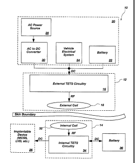
FIG. 3 is a block diagram of a TETS system in accordance with the invention.
FIG. 4 is a circuit diagram of a Class E full wave low dvldt rectifier and an
equivalent simulation model in accordance with the invention.
FIG. 5 is a graph of actual voltage waveforms from a digital oscilloscope
appearing at the diode cathodes of the circuit in FIG. 4 in accordance with
the
invention.
1 S FIG. 6 is a circuit diagram of a receiver circuit with a Class E full wave
low
dvldt rectifier and additional gating circuitry in accordance with the
invention.
FIG. 7 is a model circuit diagram of series resonant circuits in accordance
with
the invention.
FIGS. 8A and $B are actual and predicted waveforms of the output the circuit
of
FIG. 7 in accordance with the invention.
FIG. 9 is a graph of output power versus duty cycle for a TETS Class E full
wave rectifier in accordance with the invention.
FIG. 10 illustrates graphical results from the analytic model of the inductive
link
and the Class E full wave low dvldt rectifier in accordance with the
invention.
BEST MODES FOR CARRYING OUT 'THE INVENTION
FIG. 3 shows a block diagram of a transcutaneous energy transmission system
(TETS) 10 according to the invention for powering an implantable device 26.
The
implantable device 26 may be a mechanical circulatory support system (MCSS), a
left
ventricular device (LVD), a muscle stimulator, vision prosthesis, audio
prosthesis or
other implantable device requiring DC electrical power for operation. The TETS
10
includes a transmitter circuit 12 to be placed externally of the body
proximate an
CA 02348072 2001-04-20
WO 00/24456 PCT/US99/25177
_g_
implantable resonant receiver circuit 14. The terms "implantable resonant
receiver
circuit", " resonant receiver circuit" and "receiver circuit" are used
interchangeably
herein. The transmitter circuit 12 includes external TETS circuitry 16 and an
external
coil 18. The external TETS circuitry may comprise a Class D amplifier to drive
external coil 18. External coil 18 may comprise Litz wire to minimize the skin
effect,.
as is known to one of skill in the art. The external TETS circuitry 16
requires a DC
power source 20 for operation. The DC power source 20 may be a battery 22,
which
may be rechargeable. Battery 22 may comprise any battery technology, including
but
not limited to, lithium ion, nickel metal hydride, nickel cadmium and alkaline
sufficient
to power, or charge the battery of, an implanted device 26. Battery 22
provides patient
mobility for extended periods of time. Battery 22 may be integrated with the
transmitter circuit 12. The DC power source 20 may be a vehicle electrical
system 24.
A vehicle electrical system 24 may be used to power a TETS 10 and/or charge an
integrated or attached battery 22. The DC power source 20 may also be an AC
power
source 28 with an AC to DC power converter 30.
The implantable receiver circuit 14 includes an internal coil 32 and internal
TETS circuitry 34 for converting RF energy into DC electrical power for an
implantable
device 26. Internal coil 32 may comprise Litz wire to minimize the skin effect
as is
known to one of skill in the art. The implantable receiver circuit 14 is
electrically
coupled to the implantable device 26 and to an impiantable battery 36.
Implantable
battery 36 is rechargeable and may comprise any battery technology, including
but not
limited to, lithium ion, nickel metal hydride, nickel cadmium and alkaline
sufficient to
power an implanted device 26. Implantable battery 36 provides patient mobility
for
short periods of time. Irnplantable battery 36 may be integrated with the
implantable
receiver circuit 14.
Internal TETS circuitry 34 includes a Class E full wave low dvldt rectifier,
see
FIG. 4. The terms "Class E full wave low dvldt rectifier" and "Class E full
wave
rectifier" are used interchangeably herein. The variation in input capacitance
which
reduces link efficiency noted above has been overcome with frequency tracking.
By
using frequency tracking, high efficiency at all loads may be achieved. The
Class E full
wave rectifier has been incorporated into a resonant receiver circuit in a
novel way.
The theory developed by Galbraith has been extended to provide quantitative
CA 02348072 2001-04-20
WO 00/24456 PCT/US99/25177
-9-
expressions that describe the link efficiency, r)i",k. Additionally, the
relative phase of
the voltage and current in the implantable receiver circuit 14 has been
related to the
phase in the transmitter circuit 12.
The Class E full wave rectifier of the invention reduces heating in the
internal
coil 32, relative to a Class D full wave bridge rectifier. A transformer may
also be used
in conjunction with a Class E full wave rectifier to further reduce current in
the internal
coil 32.
Referring to FIG. 4, a circuit diagram of receiver circuit with a Class E full
wave low dvldt rectifier is shown. The internal coil (32 in FIG. 3) is modeled
as Ln
I 0 with a first end of the inductor tied to node A. A series matching
capacitor, Cm, has a
first end coupled to the second end of L,~ and second end coupled to node B.
Cm is
selected to achieve a resonant frequency of operation. The term Cm is used to
represent
both the electrical component (capacitor) and the capacitance value associated
with the
electrical component. The same terminology is used throughout this detailed
description when describing Cn, C,.;y and C,~. Two diodes, D, with anodes
coupled at
node C and cathodes coupled to nodes A and B. Two parallel capacitors, Cp, are
placed
in series between nodes A and B and in parallel with each diode, D. The node
common
to the parallel capacitors, C~, is tied to the common anode of the diodes and
is referred
to as node F. A first inductance, Lf, is coupled between node B and output
node E. A
second inductance, L~; is coupled between node A and output node E. A filter
capacitor, C/; is coupled between output node E and node F. The load resistor,
R,, is
coupled parallel to filter capacitor, Cf, and represents the resistance of the
implantable
device (26 of FIG. 3).
For a given power requirement, P", output voltage, V~" and operating
frequency,
f, the components of an Class E full wave low dvldt rectifier may be selected.
The load
resistance, R~, may be calculated from the following equation:
~2
RL ~ Po (3)
where R,, is measured in Ohms (S2). Peak output current, I,,, passing through
the load
resistance, R,,, can be calculated from the following equation (Ohm's Law):
CA 02348072 2001-04-20
WO 00/24456 PCT/US99/25177
-10-
V
Ic = R . (4)
G
where l,, is measured in Amperes {A). From the operating frequency,, f, we can
calculate the angular frequency, c.~, from the following equation:
w = 2~rf {5)
where co is measured in radians per second (Rad/s).
The duty cycle, D, for the Class E full wave low dvldt rectifier should not
exceed 0.5. When the D > 0.5, both diodes are conducting simultaneously, and
the
implantable receiver circuit {14 of FIG. 3) is not resonant. Additionally,
when D > 0.5,
the TETS will suffer losses in the link efficiency, rl,~~k, and tosses in the
AC to DC
conversion in the Class E full wave low dvldt rectifier itself. It is
preferable to operate
the Class E full wave low dvldt rectifier at D = 0.5. The parallel
capacitance, C~, can be
calculated from the following equation:
1
Cy 2~r~ RG
where C~ is measured in Farads (F).
The behavior of the Class E full wave low dvldt rectifier may be modeled as an
equivalent capacitance, C~.y, in series with an equivalent resistance, R,;y.
When D = 0,
the Class E full wave low dvldt rectifier does not shunt either capacitor with
the result
that the equivalent capacitance of the rectifier in the implantable receiver
circuit equals
half the parallel capacitance. When D < 0.5, both parallel capacitors appear
in series in
the Class E full wave low dvldt rectifier. As the duty cycle increases, the
equivalent
capacitance increases until, at D = 0.5, the Class E full wave low dvldt
rectifier shunts
one of the two parallel capacitors, C~, at all times. This phenomenon gives
rise to the
need for the operating frequency of the TETS to increase as the load
resistance
increases in order to maintain the efficiency of power delivery.
When D = 0.5 the conversion ratio, K;, of the DC output current,1,,, to the
root
mean squared (rms) AC input current, lA~.,", is, K, = 1.519. Given K; = 1.519
and the DC
output load current, I,,, the AC input current, IAA,", may be calculated from
the following
equation:
CA 02348072 2001-04-20
WO 00/24456 PCTNS99/25177
I~
L9c.~n - 1519
where IA~~,", is measured in rms A. The equivalent resistance, RL.y, may be
calculated
from the following equation:
_ P
REg ~ I 2
1.519
where R,,y is measured in S2. A mathematical analysis of the rectifier for D =
0.5 shows
that C,..y > C~. The equivalent capacitance, C,;4, may be calculated from the
following
equation:
CFg = 2.36~Cp (9)
An illustrative example for selecting component values for the Class E full
wave
low dvldt rectifier follows. Suppose the required output power, Po, of the
implantable
device is 50 Watts (W), the required output voltage, V~" is 15 Volts (V), the
operating
frequency, f, is S00 kHz with a duty cycle, D, of 0.5. From Eq. 3, R,, = 4.5
S2. With this
value of R~, the peak output current may be calculated, T, = 3.3 A, from Eq.
4. The
angular frequency, w = 3.14 x 10⁶ Rad/s, from Eq. S. The parallel capacitance,
C~ _
11.3 nF, using Eq. 6. Using Eqs. 7-9 and the given duty cycle, D, the
equivalent series
capacitance and resistance of the Class E full wave low dvldt rectifier may be
calculated
as C~ = 11.3 nF, C,;y = 26.6 nF and R,,~~ = I 0.4 S2.
The link efficiency, rl~~nk, may be calculated from the following equation:
k2
Mink = 1 ( 10)
kz +
~r ~n
where rl,;~~ is a number between 0 and 1 and k is the coupling coefficient as
indicated in
Eq. 2. The quality factor of the implantable receiver circuit, Q", must be
selected to
achieve a given link efficiency, rl,;~~. Eq. 10 may be solved for Q,Z:
CA 02348072 2001-04-20
WO 00/24456 PCT/US99/25177
-12-
~R = k2 , (11)
link
An illustrative example for selecting the quality factor for the implantable
receiver circuit follows. Suppose the quality factor for the transmitter
circuit, Q,. = 1 S0,
the coupling coefficient between the external coil and the internal coil, k =
0.18 and the
link efficiency, t~,;"~ = 0.95. The coupling From Eq. 11, the quality factor
of the
implantable receiver circuit is, Q,t = 3.9.
The internal coil inductance may be calculated from the expression for the
quality factor for the implantable receiver circuit:
QR = R ( 12)
Eq
Solving for L,r,
~R REq
LR = ~ (13)
where L,~ is measured in Henries (H). Continuing with the numerical example
above,
using Eq. 13, L,z = 12.9 ~H.
Finally, it is desirable to select a matching capacitance, Cm, to be place in
series
with the internal coil inductance and the Class E full wave low dvldt
rectifier to operate
the implantable receiver circuit at resonance. The resonant angular frequency
may be
calculated from the following equation:
1
r~ _ ( 14)
LR CR
where C,z is the capacitance of the implantable receiver circuit. Solving for
C,r:
1 1
CR = ~2L - 1 1 (15)
R + --_
CEq Cm
CA 02348072 2001-04-20
WO 00/24456 PCT/US99/25177
-13-
where C,t is measured in F. Again continuing with the numerical example, C,~ =
7.8 nF.
From Eq. 15 an expression for the matching capacitance, C"" may be derived:
1
Cn~ 1 1 (16)
CR CEg
where C", is measured in F. Using Eq. 16 with C,z = 7.8 nF and C~.y = 26.6 nF,
C", _
11.1 nF.
FIG. 5 is a graph of actual voltage waveforms from a digital oscilloscope
appearing at the diode cathodes of the circuit in FIG. 4 in accordance with
the
invention.
FIG. 6 illustrates a circuit diagram of an implantable receiver circuit with a
Class E full wave low dvldt rectifier and additional gating circuitry in
accordance with
the invention. The additional gating circuitry and field effect transistors
(FETs) provide
synchronous rectification to reduce diode losses. The function of the gating
circuitry is
to sense current flowing in the diodes and to turn on the transistors when the
current in
the diodes is above a threshold current. The gate control circuitry may
comprise a one
turn primary or a current sensing resistor or other means of sensing current.
The design
of gate control circuitry is within the knowledge of one of skill in the art.
FIG. 7 is a model circuit diagram of series resonant circuits in accordance
with
the invention which may be used to model a TETS. FIGS. 8A and 8B are,
respectively,
actual and predicted waveforrns of the output the circuit of FIG. 7 in
accordance with
the invention. FIG. 9 is a graph of output power versus duty cycle for a TETS
Class E
full wave rectifier in accordance with the invention. FIG. 10 illustrates
graphical results
from the analytic model of the inductive link and the Class E full wave low
dvldt
rectifier in accordance with the invention.
Although this invention has been described with reference to particular
embodiments, the invention is not limited to these described embodiments.
Rather, it
should be understood that the embodiments described herein are merely
exemplary and
that a person skilled in the art may make many variations and modifications
without
departing from the spirit and scope of the invention. All such variations and
CA 02348072 2001-04-20
WO 00/24456 PCT/US99/25177
-14-
modifications are intended to be included within the scope of the invention as
defined
in the appended claims.